 | –≠–ª–µ–∫—Ç—Ä–æ–Ω–Ω—ã–π –∫–æ–º–ø–æ–Ω–µ–Ω—Ç: SII201C | –°–∫–∞—á–∞—Ç—å:  PDF PDF  ZIP ZIP |

Revision 1.0
Subject to Change without Notice
SiI 201
C Intelligent Panel Controller
PanelLink
Æ
Digital
March 1999
General Description
Features
The
SiI 201
C Intelligent Panel Controller (IPC) uses PanelLink Digital
technology to support displays ranging from VGA to XGA (25-68 MHz), which is
ideal for LCD notebook and desktop monitor applications. With a flexible single
or dual pixel out interface and selectable output drive, the
SiI 201
C IPC supports
up to true color panels (24 bit/pixel, 16.7M colors) in 1 or 2 pixels/clock mode.
The
SiI 201
C is highly programmable to support multiple column and row drivers
and to optimize display quality. PanelLink also features an inter-pair skew
tolerance up to 1 full input clock cycle and a highly jitter tolerant PLL design.
PanelLink Digital technology simplifies PC design by resolving many of the
system level issues associated with high-speed digital design, providing the
system designer with a digital interface solution that is quicker to market and
lower in cost.
∑
Scaleable Bandwidth: 25-68 MHz (VGA to XGA)
∑
Low Power: 3.3V core operation & power-down mode
∑
High Skew Tolerance: 1 full input clock cycle (15ns at 65
MHz)
∑
Highly programmable: supports multiple column drivers
∑
Sync Detect: for Plug & Display "Hot Plugging"
∑
Cable Distance Support: over 5m with twisted-pair, fiber-
optics ready
∑
Compliant with DVI 1.0 (DVI is backwards compatible
with VESAÆ P&D
TM
and DFP)
SiI 201
C Pin Diagram
Reserved
PD
Reserved
PGND
PVCC
EXT_RES
RXC-
RXC+
AGND
RX0-
RX0+
AVCC
RX1-
RX1+
AGND
RX2-
RX2+
AVCC
GND
OVCC
VCC
CK_B
W 4 8
S C A L E _ I N
R O F F _ T ( 2 )
R O F F _ T ( 1 )
R O F F _ T ( 0 )
R O E _ T ( 1 )
R O E _ T ( 0 )
V C C
G N D
C V _ P
C O N V
P O L
O G N D
S C D T
/POL /
C D A T A 0
O V C C
Reserved /
C D A T A 1
C D A T A 2
C D A T A 3
C D A T A 4
C D A T A 5
C D A T A 6
C D A T A 7
Reserved /
C D A T A 8
PL_T /
C D A T A 9
C D A T A 3 1
C D _ E /
C D A T A 3 2
PIX_O /
C D A T A 3 3
C D A T A 3 4
C D A T A 3 5
C D A T A 3 6
C D A T A 3 7
C D A T A 3 8
C D A T A 3 9
O G N D
C D A T A 4 0
/ DINV
C D A T A 4 1
/ ST
C D A T A 4 2
C D A T A 4 3
C D A T A 4 4
C D A T A 4 5
C D A T A 4 6
V C C
C D A T A 4 7
CIN
C L T 1 /
C D I R
C L T 2 /
C I N 2
RIN
R O E
R C K
CDATA29
CDATA30
CDATA28
CDATA27
CDATA26
CK_P /
CDATA25
OGND
CCK
CV_W /
CDATA24
CDATA23
CDATA22
CDATA21
GND
CDATA20
CDATA19
CDATA18
CK_D /
CDATA17
CK_T /
CDATA16
OVCC
CDATA15
CDATA14
CDATA13
CDATA12
CDATA11
CDATA10
PDO
VCC
GND
1
2
3
4
5
6
7
8
9
10
11
12
13
14
15
16
17
18
19
20
21
22
23
24
2 5
1 0 0
99
98
97
96
95
94
93
92
91
90
89
88
87
86
85
84
83
82
81
80
79
78
77
76
7 5
74
73
72
71
70
69
68
67
66
65
64
63
62
61
60
59
58
57
56
55
54
53
52
51
26
27
28
29
30
31
32
33
34
35
36
37
38
39
40
41
42
43
44
45
46
47
48
49
SiI201C
1 0 0 P i n T Q F P
5 0
Silicon Image, Inc.
SiI 201C
SiI/DS-0005-C
Revision 1 0
2
Subject to Change without Notice
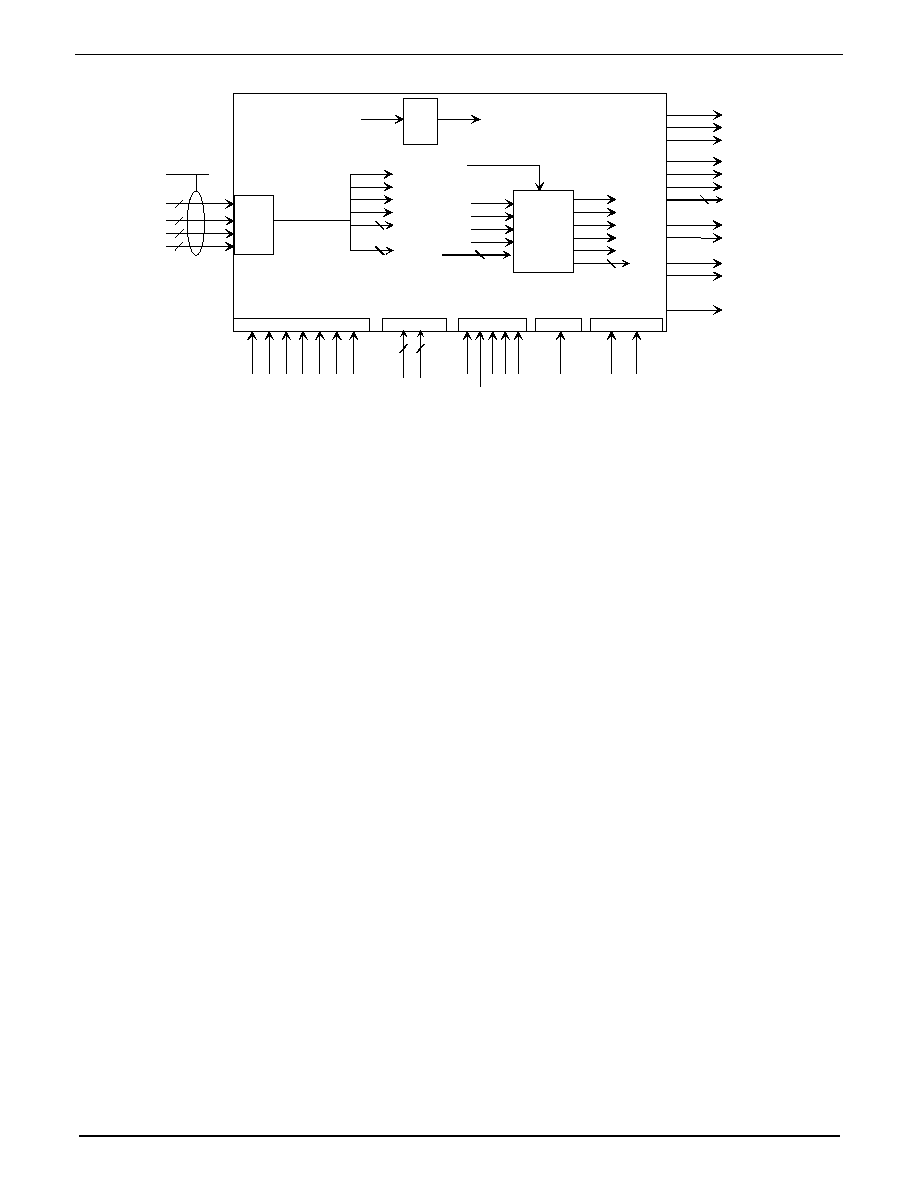
Functional Block Diagram
The SiI 201C consists of four major blocks: the Functional PanelLink Interface, Sync Detection and the Row and Column
Interface.
PanelLink
Interface: The SiI 201C accepts the
PanelLink
interface of 4 low swing, differential input signals. One
pair contains the pixel clock, the other three pairs are the serialized and encoded red, green and blue channels. Each of the
color channels also contain two encoded control signals. The
PanelLink
technology de-serializes and decodes the input
data to recover the original panel interface, labeled PPI in the block diagram. This interface is a one color pixel per clock
interface at 24 bits per pixel, the recovered input clock is ICK.
Column Interface(CIN, CCK, CONV, CDTA): The column interface block is programmed so that the column drive
outputs are set to match the desired column drivers. By programming the pins CK_P, CK_B, CK_D, CK_T, CV_W,
CV_P, PL_T and DINV a wide variety of column drivers can be addressed.
Row Interface(RIN, RCK, ROE): The row driving signals are output from this block. While the row signals require no
programmability, their timing with respect to the column drive signals is critical, and varies with panel size and processing
parameters. Sufficient time must be allowed for the row select signals to be fully switched off before the column driver's
analog outputs are allowed to change. This time T
OFF
, can be set over a wide range of values through the ROFF_T[2:0]
programming input bits. If the row driver chosen has an output enable, the width of the output enable pulse can be set
using ROE_T[1:0].
Sync Detect: This block monitors the state of HSYNC. If HSYNC becomes inactive the output signal SCDT will be set
low. This signal can be used to control driver and backlight supplies enabling panel protection and power savings.
IDTA
R X C
R X 0
R X 1
R X 2
P a n e l L i n k
Interface
2
2
2
2
P P I
C C K
C O N V
CIN
C D T A
2 4 / 4 8
V S Y N C
H S Y N C
I C K
D E
IDTA
2 4
C o l u m n C o n t r o l
CK_P
CV_W
CK_B
R o w T i m i n g
ROFF_T
ROE_T
CD_E
Polarity
PL_T
P o w e r C o n t r o l
PDO
CV_P
V S Y N C
D E
H S Y N C
I C K
4
2
3
C D I R
S y n c
D e t e c t
H S Y N C
S C D T
P O L
R C K
R O E
RIN
C C K
C O N V
CIN
C D T A
2 4 / 4 8
C T L 1 / C D I R
P O L
S C D T
C T L 2 / C I N 2
C T L
2 4
/ P O L
PIX_O
I / 0
PD
CK_D
CK_T
S C A L E _ I N
W48
ST
SCALE_IN
DINV
P e r i p h e r y
Controller
PanelLink
Technology
Silicon Image, Inc.
SiI 201C
SiI/DS-0005-C
Revision 1 0
3
Subject to Change without Notice
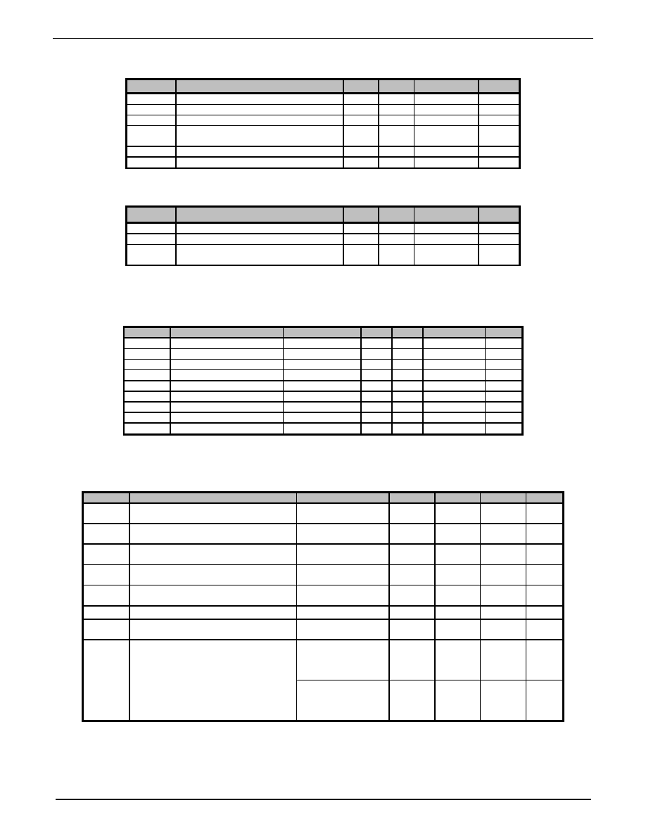
Absolute Maximum Conditions
Note: Permanent device damage may occur if absolute maximum conditions are exceeded.
Functional operation should be restricted to the conditions described under Normal Operating Conditions
.
Symbol
Parameter
Min
Typ
Max
Units
V
CC
Supply
Voltage
-0.3 -
6.0
V
V
I
Input
Voltage
-0.3 - V
CC
+ 0.3
V
V
O
Output Voltage
-0.3
-
V
CC
+ 0.3
V
T
A
Ambient Temperature
(with power applied)
-25 -
85
∞
C
T
STG
Storage
Temperature
-40 -
125
∞
C
P
PD
Package Power Dissipation
-
-
1
W
Normal Operating Conditions
Symbol
Parameter
Min
Typ
Max
Units
V
CC
Supply
Voltage
3.0 3.3
3.6
V
V
CCN
Supply Voltage Noise
100
mV
P-P
T
A
Ambient Temperature
(with power applied)
0
25 70
∞
C
Note:
1
Guaranteed by design.
DC Digital I/O Specifications
Under normal operating conditions unless otherwise specified.
Symbol
Parameter
Conditions
Min
Typ
Max
Units
V
IH
High-level Input Voltage
2
V
V
IL
Low-level Input Voltage
0.8
V
V
OH
High-level Output Voltage
2.4
V
V
OL
Low-level Output Voltage
0.4
V
V
CINL
Input Clamp Voltage
1
I
CL
= -18mA
GND -0.8
V
V
CIPL
Input Clamp Voltage
1
I
CL
= 18mA
IVCC + 0.8
V
V
CONL
Output Clamp Voltage
1
I
CL
= -18mA
GND -0.8
V
V
COPL
Output Clamp Voltage
1
I
CL
= 18mA
OVCC + 0.8
V
I
IL
Input Leakage Current
-10
10
µ
A
Note:
1
Guaranteed by design.
DC Specifications
Under normal operating conditions unless otherwise specified. Low drive strength values, when ST=0, are shown in brackets.
Symbol
Parameter
Conditions
Min
Typ
Max
Units
I
OH
(ST=0) Output High Drive (CCK)
(ST=1)
V
OUT
= V
OH
6
15
8
16.5
10.5
35
mA
I
OL
(ST=0) Output Low Drive (CCK)
(ST=1)
V
OUT
= V
OL
-8.5
-19
-12
-24
-15.4
-27
mA
I
OH
(ST=0) Output High Drive (All Others)
(ST=1)
V
OUT
= V
OH
4
9
5.5
11
7
22
mA
I
OL
(ST=0) Output Low Drive (All Others)
(ST=1)
V
OUT
= V
OL
-5.6
-9
-8
-16
-10
-11
mA
V
ID
Differential Input Voltage Single Ended
Amplitude
250
1000
mV
I
PD
Power-down
Current
1
-
50
uA
1
mA
I
PDL
Output leakage current to ground in high
impedance mode (PD, PDO = LOW)
10
uA
I
CCR
Supply Current @ 3.3V V
CC
Output is one pixel per clock mode.
2
DLCK = 65 MHz
C
LOAD
= 10pF
R
EXT_SWING
= 680
Typical Pattern
3
-
137 157 mA
DCLK = 65 MHz
C
LOAD
= 10pF
R
EXT_SWING
= 680
Worst Case Pattern
4
-
153 185 mA
Notes:
1
The transmitter must be in power-down mode, powered off, or disconnected for the current to be under this maximum.
2
For worst case I/O power consumption.
3
The Typical Pattern contains a gray scale area, checkerboard area, and text.
4
Black and white checkerboard pattern, each checker is one pixel wide.

Silicon Image, Inc.
SiI 201C
SiI/DS-0005-C
Revision 1 0
4
Subject to Change without Notice
AC Specifications
Under normal operating conditions unless otherwise specified. Low drive strength values, when ST=0, are shown in brackets.
Symbol
Parameter
Conditions
Min
Typ
Max
Units
T
DPS
Intra-Pair (+ to -) Differential Input Skew
200
ps
T
CCS
Channel to Channel Differential Input Skew
T
CIP
ns
T
IJIT
Worst Case Differential Input Clock Jitter tolerance
1,2
2 ns
D
LHT
Low-to-High Transition Time: Data and Controls
ST=1 [ST=0]
C
L
= 10pF [5pF]
1.9
[1.9]
ns
CCK
1.6
[1.4]
D
HLT
High-to-Low Transition Time: Data and Controls
ST=1 [ST=0]
C
L
= 10pF [5pF]
1.6
[1.6]
ns
CCK
1.4
[1.2]
T
SOF
Data/Control Setup Time to CCK:
4
65 MHz, One Pixel / Clock, PIXS = 0
ST=1 [ST=0]
C
L
= 10pF [5pF]
CK_T = 0
6.0
[5.8]
ns
ST=1 [ST=0]
C
L
= 10pF [5pF]
CK_T = 1
1.8 [2.1]
ns
T
HOF
Data/Control Hold Time to CCK
:
4
65 MHz, One Pixel / Clock, PIXS = 0
ST=1 [ST=0]
C
L
= 10pF [5pF]
CK_T = 0
4.9
[4.5]
ns
ST=1 [ST=0]
C
L
= 10pF [5pF]
CK_T = 1
8.9 [9.0]
ns
R
CIP
CCK Cycle Time (1 pixel/clock)
14.7
50
ns
F
CIP
CCK Frequency (1 pixel/clock)
20
68
MHz
R
CIP
CCK Cycle Time (2 pixels/clock)
29.4
100
ns
F
CIP
CCK Frequency (2 pixels/clock)
10
34
MHz
R
CIH
CCK High Time
65 MHz, One Pixel / Clock, PIXS = 0
3
ST=1 [ST=0]
C
L
= 10pF [5pF]
5.3
[4.9]
ns
R
CIL
CCK Low Time
65 MHz, One Pixel / Clock, PIXS = 0
3
ST=1 [ST=0]
C
L
= 10pF [5pF]
6.9
[6.7]
ns
T
HSC
Link disabled (HSYNC inactive) to SCDT low
50
ms
T
FSC
Link enabled (HSYNC active) to SCDT high
2
ms
T
PDL
Delay from PD/ PDO Low to high impedance outputs
8
ns
Notes:
1
Jitter can be estimated by: 1) triggering a digital scope at the rising of input clock, and 2) measuring the peak to peak time
spread of the rising edge of the input clock 1
µ
s after the trigger.
2
Actual jitter tolerance may be higher depending on the frequency of the jitter.
3
Output clock duty cycle is independent of the differential input clock duty cycle and the IDCK duty cycle.
4
The setup and hold timing for the data and controls is measured relative to CCK rising edge.
Silicon Image, Inc.
SiI 201C
SiI/DS-0005-C
Revision 1 0
5
Subject to Change without Notice
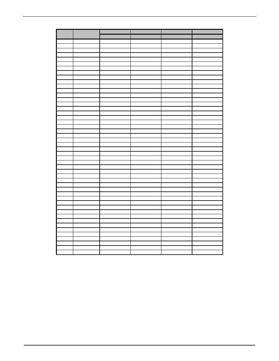
1.1 Data Bus Mapping
18-bpp
24-bpp
36-bit
48-bit
Pin #
Name
1-pixel/clock
1-pixel/clock
2-pixel/clock
2-pixel/clock
15
CDATA0
B0/E
17
CDATA1
B1/E
18
CDATA2 B0
B2
B0/E
B2/E
19
CDATA3 B1
B3
B1/E
B3/E
20
CDATA4 B2
B4
B2/E
B4/E
21
CDATA5 B3
B5
B3/E
B5/E
22
CDATA6 B4
B6
B4/E
B6/E
23
CDATA7 B5
B7
B5/E
B7/E
24
CDATA8
G0/E
25
CDATA9
G1/E
26
CDATA10
G0 G2 G0/E
G2/E
27
CDATA11
G1 G3 G1/E
G3/E
28
CDATA12
G2 G4 G2/E
G4/E
29
CDATA13
G3 G5 G3/E
G5/E
30
CDATA14
G4 G6 G4/E
G6/E
31
CDATA15
G5 G7 G5/E
G7/E
33
CDATA16
R0/E
34
CDATA17
R1/E
35
CDATA18
R0 R2 R0/E
R2/E
36
CDATA19
R1 R3 R1/E
R5/E
37
CDATA20
R2 R4 R2/E
R4/E
39
CDATA21
R3 R5 R5/E
R5/E
40
CDATA22
R4 R6 R4/E
R6/E
41
CDATA23
R5 R7 R5/E
R7/E
42
CDATA24
B0/O
45
CDATA25
B1/O
46
CDATA26
B0
B0/O
B2/O
47
CDATA27
B1
B1/O
B3/O
48
CDATA28
G0
B2/O
B4/O
49
CDATA29
G1
B3/O
B5/O
50
CDATA30
R0
B4/O
B6/O
51
CDATA31
R1
B5/O
B7/O
52
CDATA32
G0/O
53
CDATA33
G1/O
54
CDATA34
G0/O
G2/O
55
CDATA35
G1/O
G3/O
56
CDATA36
G2/O
G4/O
57
CDATA37
G3/O
G5/O
58
CDATA38
G4/O
G6/O
59
CDATA39
G5/O
G7/O
61
CDATA40
R0/O
62
CDATA41
R1/O
63
CDATA42
R0/O
R2/O
64
CDATA43
R1/O
R3/O
65
CDATA44
R2/O
R4/O
66
CDATA45
R3/O
R5/O
67
CDATA46
R4/O
R6/O
69
CDATA47
R5/O
R7/O
Legend :
1. R = RED Channel, G = GREEN Channel, B = BLUE Channel.
2. /E = EVEN (first) pixel data (P0, P2, P4, etc.)
3. /O = ODD (second) pixel data (P1, P3, P5, etc.)
Assumptions on how
PanelLink
is connected :
1. Bits 7:0 mapped MSB:LSB.
2. Tx0/Rx0 transmits BLUE (B) data.
3. Tx1/Rx1 transmits GREEN (G) data.
4. Tx2/Rx2 transmits RED (R) data