
© 2003 QuickLogic Corporation
www.quicklogic.com
∑
∑
∑
∑
∑
∑
1
∑ ∑ ∑ ∑ ∑ ∑
Device Highlights
High Performance PCI Controller
∑
32-bit / 33 MHz PCI Master/Target with
Embedded Programmable Logic
∑
Zero-wait state PCI Master provides 132 MBps
transfer rates
∑
Programmable back-end interface to optional
local processor
∑
Independent PCI bus (33 MHz) and local bus (up
to 160 MHz) clocks
∑
Fully Customizable PCI Configuration Space
∑
Reference design with driver code
(Win 95/98/Win 2000/NT4.0) available
∑
PCI v2.2 compliant
∑
Supports Type 0 Configuration Cycles in Target
mode
∑
3.3 V, 5 V tolerant PCI signaling supports
Universal PCI Adapter designs
∑
High performance PCI controller 3.3 V CMOS in
208-pin PQFP and 144-pin TQFP packages
∑
Supports unlimited/continuous burst transfers
Extendable PCI Functionality
∑
Support for Configuration Space from 0 ◊ 40 to
0 ◊ 3FF
∑
Multi-Function, Expanded Capabilities, and
Expansion ROM capable
∑
Power Management, Compact PCI,
Hot-Swap/Hot-Plug compatible
∑
PCI v2.2 Power Management Specification
compatible
∑
PCI v2.2 Vital Product Data (VPD) configuration
support
∑
Programmable Interrupt Generator
∑
I
2
O Support with local processor
∑
Mailbox Register support
Programmable Logic
∑
387 Logic Cells
∑
250 MHz 16-bit counters and 275 MHz
datapaths
∑
All back-end interface and glue-logic can be
implemented on chip
∑
Three 32-bit bus interfaces between the PCI
Controller and the Programmable Logic
Figure 1: QL5022 Block Diagram
Architecture Overview
The QL5022 device in the QuickLogicÆ QuickPCITM
ESP (Embedded Standard Product) family provides a
complete and customizable PCI interface solution
combined with 25,000 system gates
of programmable
logic. This device eliminates any need for the designer
to worry about PCI bus compliance, yet allows for the
maximum 32-bit PCI bus bandwidth (132 MBps).
The programmable logic portion of the device contains
387 QuickLogic logic cells.
The QL5022 device meets PCI 2.2 electrical and
timing specifications and has been fully hardware-
tested.
The QL5022 device features 3.3 V operation with
multi-volt compatible I/Os. Thus, it can easily operate
in 3 V systems and is fully compatible with 3.3 V, 5 V,
or Universal PCI card development.
PCI Bus
PCI Bus 33 MHz/32 bits (data and
address)
Target
Controller
Config
space
DMA
Controller
Master
Controller
High Speed
Logic Cells
High
Speed
Data
Path
Programmable
Logic
32 bit Interface
116/63 User I/O
PCI Controller
QL5022 QuickPCI Data Sheet
33 MHz/32-bit PCI Host Capable Master Target with Embedded
Programmable Logic

www.quicklogic.com
© 2003 QuickLogic Corporation
∑
∑
∑
∑
∑
∑
QL5022 QuickPCI Data Sheet Rev B
2
PCI Controller
The PCI Controller is a 32-bit/33 MHz PCI 2.2 Compliant Master/Target Controller. It is capable
of infinite length Master Write and Read transactions at zero wait state (132 MBps). The Master
will never insert wait states during transfers, so data should be supplied or received by the logic in
the programmable region of the device. The Master Controller will most often be operated by a
DMA Controller in the programmable region of the device. A DMA Controller reference design
is available. The Target interface offers full PCI Configuration Space and flexible target
addressing. Any number of 32-bit BARs may be configured, as either memory or I/O space. All
required and optional PCI 2.2 Configuration Space registers can be implemented within the
programmable region of the device. A reference design of a Target Configuration and Addressing
module is provided.
The interface ports are divided into a set of ports for master transactions and a set for target
transactions. The Master DMA controller and Target Configuration Space and Address Decoding
are done in the programmable logic region of the device. Since these functions are not timing
critical, leaving these elements in the programmable region allows the greatest degree of flexibility
to the designer. References to DMA controller, Configuration Space, and Address Decoding
blocks are included so that the design cycle can be minimized.
Configuration Space and Address Decode
The configuration space is completely customizable in the programmable region of the device.
PCI address and command decoding is performed by logic in the programmable section of the
device. This allows support for any size of memory or I/O space for back-end logic. It also allows
the user to implement any subset of PCI commands supported by the QL5022. QuickLogic
provides a reference Address Register/Counter and Command Decode block.
DMA Master/Target Control
The customizable DMA controller included with the QuickWorksÆ design software contains the
following features:
∑
Supports DMA transfer from PCI to external
∑
Configurable DMA burst size for PCI
∑
DMA Registers may be mapped to any area of Target Memory Space
∑
Read Address (32-bit register)
∑
Read Length (16-bit register)
∑
Control and Status (32-bit register, includes 2 bit Burst Length)
∑
DMA Registers are available to the local design or the PCI bus
∑
Programmable Interrupt Control to signal end of transfer or other event
© 2003 QuickLogic Corporation
www.quicklogic.com
∑
∑
∑
∑
∑
∑
QL5022 QuickPCI Data Sheet Rev B
3
Internal PCI Interface
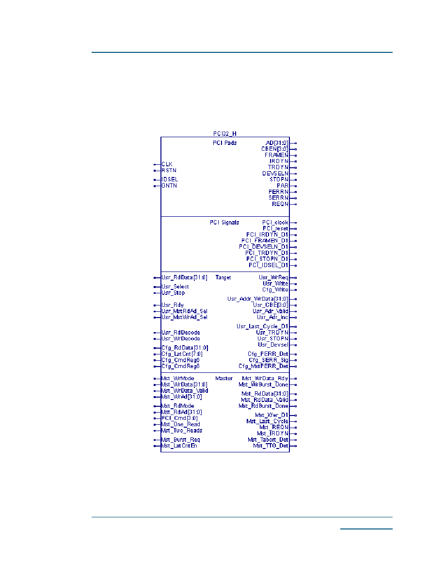
Figure 2
shows the interface symbol you will use in your schematic design to attach the local
interface programmable logic design to the PCI core. If you were designing with a top-level
VerilogÆ or VHDL file, then you would use a structural instantiation of this PCI32 block, instead
of a graphical symbol.
Figure 2: PCI Interface Symbol
www.quicklogic.com
© 2003 QuickLogic Corporation
∑
∑
∑
∑
∑
∑
QL5022 QuickPCI Data Sheet Rev B
4
PCI Master Interface
Table 1
lists the internal signals used to interface with the PCI controller in the QL5022 along
with a description of each signal. The direction of the signal indicates if it is an input provided by
the local interface (I) or an output provided by the PCI controller (O). Signals that end with the
character `N' should be considered active-low (for example, Mst_IRDYN).
Table 1: PCI Controller Signals
Signal
I/O
Description
Mst_WrAd[31:0]
I
Address for master DMA Writes
. This address must be treated as valid from
the beginning of a DMA burst write until the DMA write operation is complete.
It must be incremented by four each time data is transferred on the PCI bus, since
only DWORD (4 byte) transfers are supported.
Mst_RdAd[31:0]
I
Address for master DMA Reads
. This address must be treated as valid from
the beginning of a DMA burst read until the DMA read operation is complete. It
must be incremented by four each time data is transferred on the PCI bus, since
only DWORD (4 byte) transfers are supported.
Mst_WrMode
I
DMA state machine in Write mode
. This must be asserted at the beginning
of a Master Transfer, and must be held until the Master Transfer completed
(Mst_WrBurst_Done).
Mst_RdMode
I
DMA state machine in Read mode
. This must be asserted at the beginning
of a Master Transfer, and must be held until the Master Transfer completed
(Mst_RdBurst_Done).
Mst_Burst_Req
I
Request use of the PCI bus
. This signal should be held from when the DMA
controller is ready to provide the first data, until the transfer is complete
(Mst_WrBurst Done or Mst_RdBurst_Done).
Mst_One_Read
I
This signals to the PCI core that one data transfer remains in the burst. This
signal must be asserted when only one DWORD remains to be transferred on
the PCI bus.
Mst_Two_Reads
I
Two or less data transfers remain in the burst. This signal must be asserted when
two or less DWORDs remain to be transferred on the PCI bus.
Mst_WrData[31:0]
I
Data for master DMA writes (to PCI bus).
Mst_WrData_Valid
I
Data valid on Mst_WrData[31:0].
Mst_WrData_Rdy
O
Data receive acknowledge for Mst_WrData[31:0]. This serves as a POP control
for a FIFO which provides data to the PCI core.
Mst_WrBurst_Done
O
Master Write pipeline is empty, which indicates that the Write burst transaction
is completed.
Mst_RdData[31:0]
O Data for master DMA reads (from PCI bus).
Mst_RdData_Valid
O
Data valid on Mst_RdData[31:0]. This serves as a PUSH control for a FIFO that
receives data from the PCI core.
Mst_RdBurst_Done
O
Master read pipeline is empty, which indicates that Read burst transaction is
completed.

© 2003 QuickLogic Corporation
www.quicklogic.com
∑
∑
∑
∑
∑
∑
QL5022 QuickPCI Data Sheet Rev B
5
PCI_Cmd[3:0]
I
PCI command to be used for the master transaction.
This signal must
remain unchanged throughout the period when Mst_Burst_Req is active. PCI
commands considered as Reads include Interrupt Acknowledge, I/O Read,
Memory Read, Configuration Read, Memory Read Multiple, Memory Read Line.
PCI commands considered as Writes include Special Cycle, I/O Write, Memory
Write, Configuration Write, Memory Write and Invalidate. Users should make
sure that only valid PCI commands are supplied.
Mst_LatCntEn
I
Enable Latency Counter.
Set to 0 to ignore the Latency Timer in the PCI
configuration space (offset 0Ch). For full PCI compliance, this port should be
always set to 1.
Mst_Xfer_D1
O
Data was transferred on the previous PCI clock. Useful for updating DMA
transfer counts on DMA Read operations.
Mst_Last_Cycle
O Active during the last data transfer of a PCI master transaction.
Mst_REQN
O
The PCI REQN signal generated by this device as PCI master. Not usually used
in the back-end design.
Mst_IRDYN
O
The PCI IRDYN signal generated by this device as PCI master. Not usually used
in the back-end design.
Mst_Tabort_Det
O
Target abort detected during master transaction. This is normally an error
condition to be handled in the DMA controller.
Mst_TTO_Det O
Target timeout detected (no response from target). This is normally an error
condition to be handled in the DMA controller.
Table 1: PCI Controller Signals (Continued)