 | –≠–ª–µ–∫—Ç—Ä–æ–Ω–Ω—ã–π –∫–æ–º–ø–æ–Ω–µ–Ω—Ç: EZ4021-FC | –°–∫–∞—á–∞—Ç—å:  PDF PDF  ZIP ZIP |
June 2000
1
Copyright © 1999, 2000 by LSI Logic Corporation. All rights reserved.
MiniRISC
Æ
EZ4021-FC
EasyMACRO Microprocessor
Preliminary Datasheet
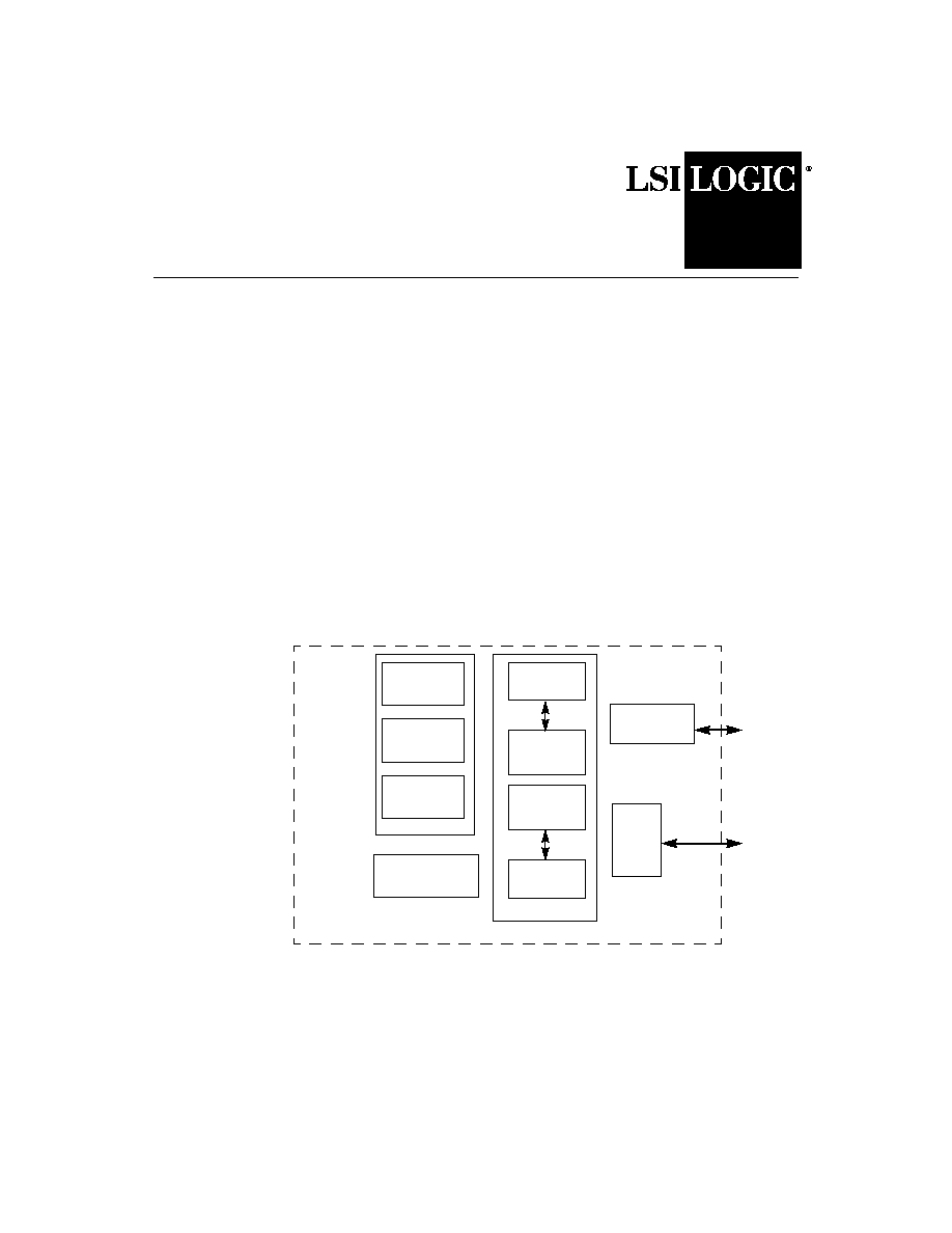
The MiniRISC EZ4021-FC Microprocessor EasyMACRO is a compact,
high-performance, 64-bit microprocessor subsystem implemented in
G12TM CMOS technology. The EZ4021-FC uses the LSI Logic
CoreWare
Æ
system-on-a-chip methodology and executes the MIPS III
instruction set. It is ideal for high-performance, cost-sensitive embedded
processor applications. As shown in
Figure 1
, the EZ4021-FC includes
the following components:
Figure 1
EZ4021-FC Microprocessor EasyMACRO Block
Diagram
∑
CPU includes system
coprocessor, an integer data
path with multiply divide unit,
and a master pipeline
controller
∑
Instruction and data caches
∑
Memory Management Unit
(MMU)
∑
Bus Interface Unit (BIU)
∑
Quick Bus interface
∑
EJTAG Interface module
CPU
Coprocessor 0
(CP0)
Integer Data
Path
(IDP)
Master Pipeline
Control
(MPC)
Instruction
Cache
Data
Cache
Caches
Memory
Management Unit
(MMU)
Bus
Interface
Unit
(BIU)
Quick Bus
Optional
Modules
EJTAG
JTAG
EZ4021-FC
Interface
Instruction
Cache
Controller
Data
Cache
Controller
EasyMACRO
ez4021ds.fm Page 1 Friday, May 26, 2000 8:27 AM

2
MiniRISC
Æ
EZ4021-FC EasyMACRO Microprocessor
Features
∑
High-performance RISC CPU
≠
Single issue, five-stage pipeline
≠
250 native MIPS, 275 Dhrystone
MIPS at 250 MHz
≠
250 MHz operation at WCABS (Tj =
125
∞
C, VDD = 1.71V, WC process)
≠
Both big- and little-endian support
for load and store operations
≠
R4000 standard 32-bit
timer/counter
≠
MIPS CPU standard interrupt
exceptions (one NMI, one timer,
five hardware, two software)
∑
Integrated multiply and divide unit
≠
High-performance eight bit/cycle
multiplier
32-bit signed/unsigned multiply
in five CPU clock cycles
64-bit signed/unsigned multiply
in nine CPU clock cycles
≠
Compact one bit/cycle divider
32-bit signed/unsigned divide in
34 CPU clock cycles
64-bit signed/unsigned divide in
66 CPU clock cycles
∑
Windows CE compatible MMU with 32
dual-entry page translations
∑
Integrated instruction and data caches
≠
Harvard architecture
≠
16 Kbyte 2-way set-associative
instruction and data caches
LRU algorithm for replacement
Line level lock for instruction
RAM and scratchpad memory
Data cache has write-through or
write back update policy,
programmable on a page basis
∑
MIPS III Instruction Set Architecture
≠
MIPS III ISA supporting 64-bit
integer operations
≠
Thirty-two 64-bit general-purpose
registers
≠
R4000-style status register and
exception processing
≠
Wait for Interrupt (WAITI) instruction
for power saving
≠
Supports SPECIAL2 Multiply-
Accumulate extensions
∑
Advanced Debug Support
≠
MIPS EJTAG version 1.5.3
≠
Instruction and data breakpoints
≠
Program Counter (PC) trace
≠
Processor singlestep and software
debug breakpoints
ez4021ds.fm Page 2 Friday, May 26, 2000 8:27 AM

MiniRISC
Æ
EZ4021-FC EasyMACRO Microprocessor
3
Features continued
Functional Description
The EZ4021-FC CPU performs all arithmetic, logical, shift, and address
calculations. The CPU includes:
∑
Data path and control
Contains a 64-bit integer data path module with a 32 x 64-bit register
file and an instruction decoder/data path control module.
∑
Integrated Multiply/Divide Unit (MDU)
Supports the MIPS accumulate operations (MADD, MADDU, MSUB,
and MSUBU) and the three-operand multiply (MUL). The MDU
includes an eight-bits-per-cycle multiply capability and a one-bit-per-
cycle divide capability.
∑
System control coprocessor (CP0)
Provides exception processing support using the MIPS R4000
exception model and processor state control that includes three
operating modes--kernel, user, supervisor.
The EZ4021-FC interface supports a new high-performance, on-chip bus
known as the Quick Bus. The Quick Bus is a split-transaction bus that
allows the overlap of memory requests (fetch/load/store) and data
returns. A Quick Bus design operating at 125 MHz can achieve a peak
bandwidth of 1.0 Gbytes per second.
The Bus Interface Unit (BIU) passes address/data between the CPU and
the Quick Bus and arbitrates CPU-to-Quick Bus access. It provides a 64-
bit incoming datapath from the Quick Bus to the CPU and a 64-bit path
for outgoing data. Depending on the customer design, outgoing Quick
Bus data can go to a variety destinations outside the EZ4021-FC.
∑
Technology
≠
2.6 mW/MHz power consumption
(includes caches)
≠
12 mm
2
core size
≠
1.8 V Core VDD
≠
LSI Logic G12 CMOS technology
(0.18
µ
L-drawn, 0.15
µ
L-effective)
ez4021ds.fm Page 3 Friday, May 26, 2000 8:27 AM

4
MiniRISC
Æ
EZ4021-FC EasyMACRO Microprocessor
The EZ4021-FC has separate instruction and data caches (I-Cache and
D-Cache). Each cache is organized as a two-way set associative
16 Kbyte cache with a fixed cache block (line) size of 8 words (32-bytes).
The caches are virtually indexed and physically tagged.
The memory management unit (MMU) performs virtual-to-physical
address translation using a 32-entry joint translation lookaside buffer
(TLB). The MMU supports a variety of page sizes from 4 Kbytes to
1 Mbyte.
The EZ4021-FC includes a Joint Test Action Group (JTAG) interface and
supports Enhanced JTAG (EJTAG) functions. EJTAG is a debug feature
of MIPS-based processors. You can use EJTAG to debug stand-alone
processors as well as 32-bit or 64-bit processors that are embedded in
a system like the EZ4021-FC.
Pipeline Architecture
The EZ4021-FC five-stage instruction pipeline is illustrated in
Figure 2
.
Figure 2
EZ4021-FC Instruction Pipeline
Instruction fetch occurs during the first two pipeline stages and
instruction execution during the last three stages. After a stage accepts
an instruction from the previous stage, it must hold the instruction for
re-execution in case the pipeline stalls. The function of each pipeline
stage is summarized below.
Instruction Fetch (I) ≠ The EZ4021-FC fetches the instruction during
this first stage.
Register Read (R) ≠ In the R stage, the CPU reads any required
operands from the Register File while decoding the instruction.
Instruction Fetch
Instruction Execution
X
M
R
I
W
ez4021ds.fm Page 4 Friday, May 26, 2000 8:27 AM

MiniRISC
Æ
EZ4021-FC EasyMACRO Microprocessor
5
Execute (X) ≠ Computational and logical instructions execute during the
X stage. The CPU resolves conditional branches during this stage, and
does the address calculations for load and store instructions.
Memory Access (M) ≠ In this stage, the CPU accesses the cache for
load and store instructions. Data returns to the register bypass logic at
the end of the M stage.
Write Back (W) ≠ The CPU writes results into the Register File in the W
stage.
Application Examples
The EZ4021-FC is designed for mid- to high-end applications, including
set top boxes and image-processing engines, networking
switches/routers, and consumer products requiring 64-bit performance.
CoreWare Program
The CoreWare program consists of three main elements:
1.
A library of cores
2.
A design development and simulation package
3.
Expert applications support
The CoreWare library contains a wide range of complex cores based on
accepted and emerging industry standards from high-speed interconnect
and digital video to DSP and MIPS microprocessors. LSI Logic provides
a complete framework for device and system development and
simulation. LSI Logic has advanced ASIC technologies that consistently
produce Right-First-TimeTM silicon. The LSI Logic in-house experts
provide design support from system architecture definition through chip
layout and test vector generation.
ez4021ds.fm Page 5 Friday, May 26, 2000 8:27 AM