February 2001
1
Copyright © 2000, 2001 by LSI Logic Corporation. All rights reserved.
G12TM-p bd4f5fs60ls33
4 mA, 60 MHz, 5-Volt Tolerant,
Fail-Safe I/O Buffer
Datasheet
The
bd4f5fs60ls33
bidirectional buffer cell (
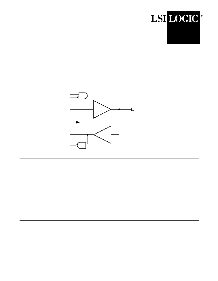
Figure 1
) provides up to
60 MHz off-chip input/output (I/O) signaling for application-specific
integrated circuit (ASIC) chips implemented in the LSI Logic G12TM-p
0.13
µ
m process technology. One application of the
bd4f5fs60ls33
buffer is as a clock driver.
Figure 1
bd4f5fs60ls33 Block Diagram
Features and Benefits
General Description
The
bd4f5fs60ls33
bidirectional I/O buffer contains a totem-pole type
driver, a receiver, and test circuitry. Included level translation circuitry
enables the driver to receive 1.8 V level signals from the ASIC circuitry
PI
TN
EN
A
Z
PO
IO
IDDTN
Chip I/O Pad
Receiver
Driver
∑
60 MHz, 3.3 V I/O operation
∑
5-Volt tolerant
∑
Fail-safe at high voltages
∑
Feedthrough protection
∑
20
µ
A maximum leakage current
∑
Minimum 4 mA current drive
into a 40 pF load at 60 MHz
∑
1.8 V internal signaling for
reduced power consumption
∑
Uses one standard I/O slot

2
G12TM-p bd4f5fs60ls33 4 mA, 60 MHz, 5-Volt Tolerant, Fail-Safe I/O Buffer
and produce 3.3 V level output at the I/O pad. Similarly, the receiver
receives off-chip input at 3.3 volts and translates it to 1.8 volts for the
internal ASIC application. Built-in NAND-tree logic gates and IDDTN
control for IDDQ leakage testing enable use of the standard LSI Logic
test methodology.
The buffer is 5-volt tolerant. Although the off-chip I/O signaling normally
operates at 3.3 V, external circuitry may cause higher voltages, typically
upwards of 5 V, to appear at the chip I/O pad. Circuit and process
techniques ensure that such DC or transient voltages do not damage the
buffer circuitry.
In the absence of a V
DD
supply, the buffer is fail-safe and protected
against voltage feedthrough. With high voltage applied to the chip I/O
pad, the buffer can survive without degradation for up to ten years.
Furthermore, with a low, maximum 20
µ
A leakage current, the high
voltage can not power up the ASIC through voltage feedthrough.
The following sections describe the
bd4f5fs60ls33
buffer, which
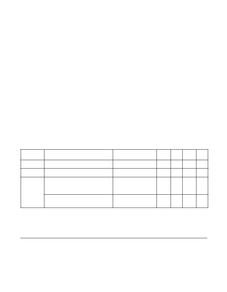
adheres to the general specifications in
Table 1
.
The final section,
"System Design Guidelines"
, provides layout guidelines
to ensure good signal integrity for applications using the noise-sensitive,
high-speed cells.
Signal Descriptions
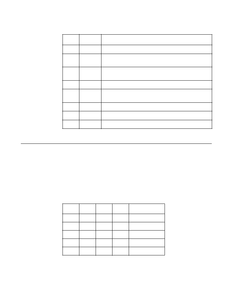
Table 2
describes the
bd4f5fs60ls33
connections.
Table 1
General Specifications
Symbol
Parameter
Condition
Min.
Typ. Max.
Unit
V
DD
Supply voltage
2.97
3.3
3.63
V
T
j
Junction temperature
0
≠
125
∞C
ESD
Electrostatic discharge,
human body model (HBM)
MIL-STD-883C,
Method 3015.7
100 pF @1.5 K
2000
≠
≠
V
Electrostatic discharge,
charged device model (CDM)
ESD DS5.3.1-1996
500
≠
≠
V

G12TM-p bd4f5fs60ls33 4 mA, 60 MHz, 5-Volt Tolerant, Fail-Safe I/O Buffer
3
Driver
The following sections describe the driver side of the I/O buffer.
Truth Table
Table 3
describes the
bd4f5fs60ls33
driver behavior.
Table 2
bd4f5fs60ls33 Connections
Signal
Direction
Description
A
IN
Data input to driver from ASIC circuitry
EN
IN
0 = Normal mode
1 = Disable driver
IDDTN
IN
0 = Power down entire cell
1
1 = Normal mode
1. Used for production IDDQ leakage test
PI
IN
NAND-tree parametric test input
TN
IN
0 = Disable driver
1 = Normal mode
IO
IN/OUT
Input/output pad
PO
OUT
NAND-tree parametric test output
Z
OUT
Receiver buffer output to ASIC circuitry
Table 3
Driver Truth Table
IDDTN
A
TN
EN
IO
0
1
1. Factory IDDQ test setting
X
2
2. Don't care state, X = 0 or 1
X
X
High Impedance
1
X
X
1
High Impedance
1
X
0
X
High Impedance
1
0
1
0
0
1
1
1
0
1

4
G12TM-p bd4f5fs60ls33 4 mA, 60 MHz, 5-Volt Tolerant, Fail-Safe I/O Buffer
Driver Specifications
DC Characteristics
Table 4
describes the
bd4f5fs60ls33
driver DC characteristics.
Driver Slew Rate
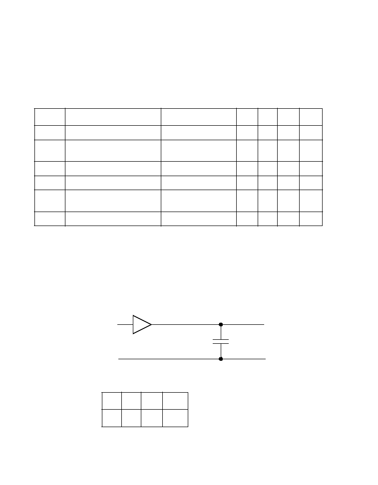
In the rise/fall test, the driver drives a signal across a 40 pF load
capacitor (
Figure 2
).
Table 5
shows the observed slew rate across the
load capacitor measured from 0.6 V to 2.2 V.
Figure 2
Rise/Fall Test Circuit
Table 4
Driver DC Characteristics
1
1. Values apply over all voltage, temperature, and process conditions.
Symbol
Parameter
Test Condition
Min.
Typ. Max.
Units
V
OL
Output, LOW
I
OL
= 4 mA
≠
≠
0.4
V
V
OH
Output, HIGH
I
OH
=
-
4 mA
V
DD
= 3.135 V
2.4
≠
≠
V
I
OL
Sink current
V
OL
= 0.4 V maximum
4
≠
≠
mA
I
OH
Source current
V
OH
= 2.4 V minimum
≠
≠
-
4
mA
I
OZ
3-Stated leakage current
0
V
PAD
5.5 V,
V
DD
= 3.3 V
±
10%
≠
≠
20
µ
A
I
LU
Latchup current
-
2 V < V
PAD
< +8 V
≠
≠
±
100
mA
Table 5
Driver Rise/Fall Slew Rate
Min. Typ. Max.
Unit
500
880
1500
mV/ns
Output
40 pF
Input
GND

G12TM-p bd4f5fs60ls33 4 mA, 60 MHz, 5-Volt Tolerant, Fail-Safe I/O Buffer
5
Receiver
The following sections describe the receiver side of the I/O buffer.
Truth Table
Table 6
describes the
bd4f5fs60ls33
receiver behavior.
Receiver Specifications
Table 7
describes the
bd4f5fs60ls33
receiver DC characteristics.
Table 6
Receiver Truth Table
Inputs
Outputs
IDDTN
IO
PI
Z
PO
0
1
1. Factory IDDQ test setting
High Impedance 1
1
0
1
0
0
0
1
1
1
0
1
1
1
1
1
1
0
Table 7
Receiver DC Characteristics
1
1. Values apply over all voltage, temperature, and process conditions
Symbol
Parameter
Test Condition
Min.
Typ.
Max.
Units
V
IL
Threshold, HIGH-to-LOW
1.0
≠
1.50
V
V
IH
Threshold, LOW-to-HIGH
1.50
≠
2.0
V
V
TH
≠V
TL
Hysteresis
320
≠
≠
mV
I
LU
Latch-up current
-
2 V < V
PAD
< +8 V
≠
≠
±
100
mA
