iC-VR
BIDIRECTIONAL µP INTERFACE TO 24V
Rev A1, Page 1/12
PLCC44
FEATURES
APPLICATIONS
À
2 ◊ 4 bidirectional input/output stages at 24 V
À
Input/output mode programmable for each 4 bits
À
Guaranteed low-side driving capability of 100 mA
dc
and
500 mA
peak
for pulse load
À
Short-circuit-proof driver with high electric strength
up to 48 V
À
Low saturation voltage of 0.4 V at 10 mA and
1.5 V at 500 mA
À
Programmable pull-down current sources
À
Built-in free-wheeling diodes with externally accessible
common cathode
À
Flashing function for the outputs
À
Programmable digital input filters with externally adjusted
filtering times
À
Bus capability via high-speed microprocessor interface
À
Programmable interrupt output
À
Shutdown at overtemperature and low voltage
À
Dual quad low-side driver as
bidirectional µP interface with
digital filtering in 24 V industrial
applications
PACKAGES
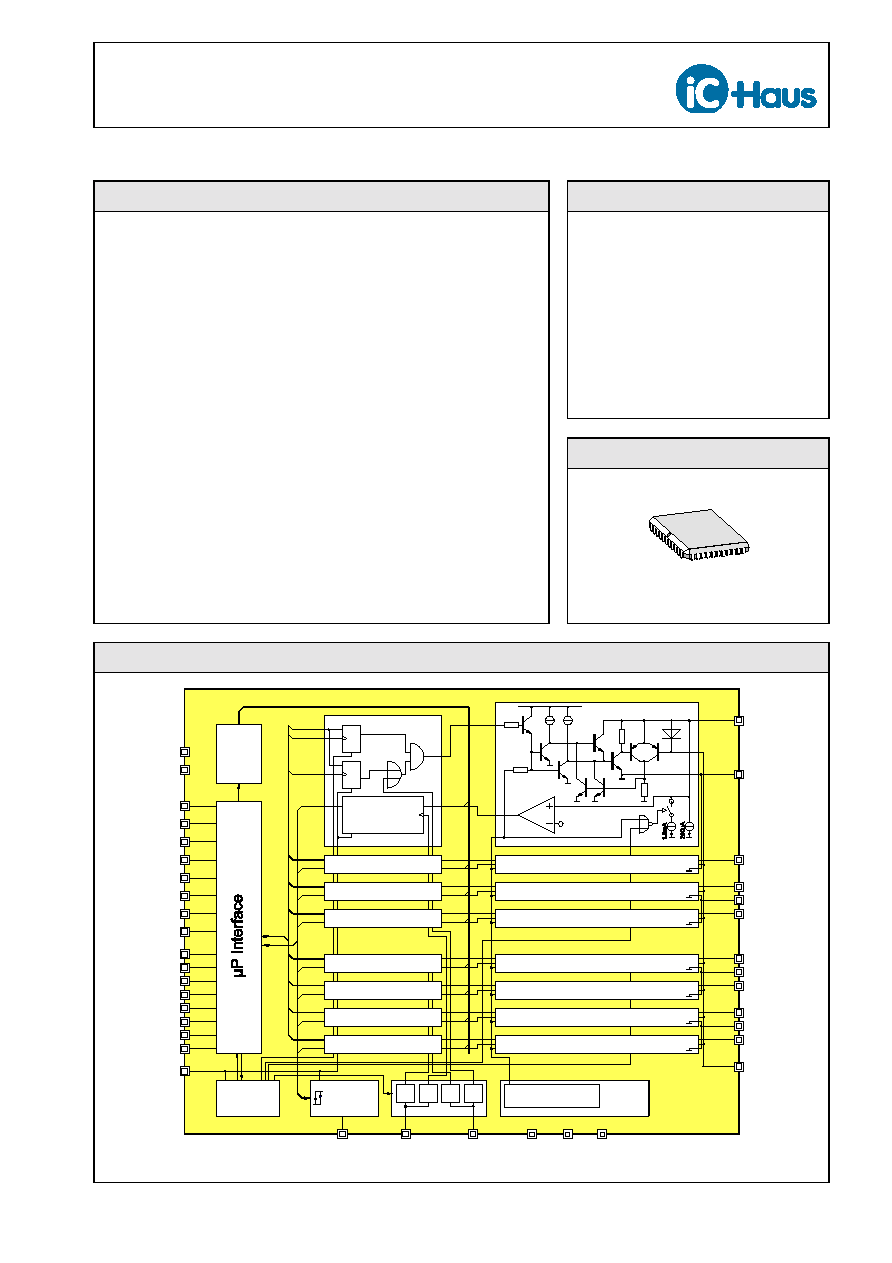
BLOCK DIAGRAM
Copyright © 2003, iC-Haus
www.ichaus.com
iC-VR
Register
Input/Output Stage 7
Input/Output Stage 6
Input/Output Stage 5
Input/Output Stage 4
Input/Output Stage 3
Input/Output Stage 2
Input/Output Stage 1
I/O Logic
I/O Logic
I/O Logic
I/O Logic
I/O Logic
I/O Logic
I/O Logic
DISABLE
higher nibble
lower nibble
Q
Input/Output Stage 0
VCC-1.3V
Bias
Thermal Shutdown
Low Voltage
Frequency Divider
Interrupt
R
Bln
DIV
Bhn
DIV
Cln
DIV
Chn
DIV
D
D
Q
NQ
R
R
Control
Test
Input Filter
Output Latch
up/dwn
3 Bit Counter
CTEST
ENERR
CERR
GNDA
GNDS
GNDD
D0
D1
D2
D3
D5
D6
IO0
GND01
IO1
IO2
GND23
IO3
IO4
GND45
IO5
IO6
GND67
IO7
COM
BLFQ
CLK
INTN
RESN
D7
D4
RDN
WRN
VCCD
VCCA
CSN
A0
A1
34
30
6
4
41
7
44
39
2
3
40
42
43
1
35
36
37
38
8
11
10
9
12
13
16
24
25
26
27
28
23
22
21
20
19
18
17
29
PLCC44

iC-VR
BIDIRECTIONAL µP INTERFACE TO 24V
Rev A1, Page 2/12
DESCRIPTION
iC-VR is an 8-fold low-side driver with integrated control logic which is divided internally into two mutually
independent blocks (nibbles).
In the input mode, ports IO0 to IO7 can be used to record logical levels. In this process, a programmable
pull-down current (200 µA or 2 mA) sets a defined level and functions as the biasing current for switching
contacts. The stages programmed as outputs can drive any desired loads (e. g. lamps, long cables, relays)
at a continuous current of 100 mA or 500 mA in pulse operation. The free-wheeling currents created upon
each stage turn-off are discharged through the integrated free-wheeling diodes to a voltage applied externally
to the COM pin; a circuit with a Zener diode is also possible.
In the event of a short circuit, a protective circuit breaker ensures that the output stage affected does not just
simply switch off but is instead clocked as a function of the load. As a result, the current assumes a low
average value. The output stage is ready for operation immediately just as soon as the cause of the short
circuit has been eliminated.
The shutdown at overtemperature protects the IC against thermal destruction by causing the output stages
to turn off and the pull-down currents to be reduced from 2 mA to 200 µA. This shutdown is also triggered in
case of undervoltage at VCC.
Due to the microprocessor interface the iC-VR can be operated directly on a bus system. The interface
consists of the data bits D0 to D7 and the associated control signals A0, A1, CSN, WRN and RDN. The signal
CLK clocks the implemented digital input filter and BLFQ clocks the programmed flashing function. In the
event of a signal change of the I/O pins programmed as inputs, an interrupt signal can be generated at output
INTN.
Activating the input RESN resets the initial condition.
Chip programming is conducted via four addresses at A0 and A1. During this programming, presettings for
flashing frequencies, filtering times, interrupt control, pull-down currents and input/output mode, etc. are stored
in two registers (CONTROL WORD1+2).
All inputs and outputs are protected with diodes against destruction due to ESD.
iC-VR
BIDIRECTIONAL µP INTERFACE TO 24V
Rev A1, Page 3/12
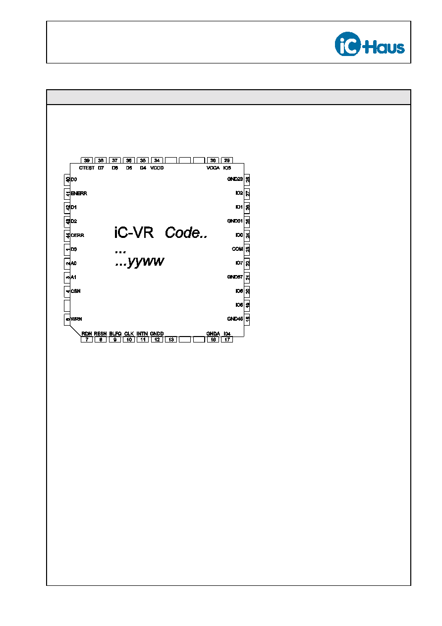
PACKAGES PLCC44 to JEDEC Standard
PIN CONFIGURATION PLCC44
(top view)
PIN FUNCTIONS PLCC44
No.
Name
Function
Description
No.
Name
Function
Description
1
D3
B
Bus Data Bit 3
23
COM
Diodes, common cathode
2
A0
I
Address
24
IO0
B
I/O Stage 0
3
A1
I
Address
25
GND01
Ground Stage 0+1
4
CSN
I
Chip Select
26
IO1
B
I/O Stage 1
5
n.c.
27
IO2
B
I/O Stage 2
6
WRN
I
Write Enable
28
GND23
Ground Stage 2+3
7
RDN
I
Read Enable
29
IO3
B
I/O Stage 3
8
RESN
I
Reset
30
VCCA
+5 V Supply (analog section)
9
BLFQ
I
Clock, flashing function
31
n.c.
10
CLK
I
Clock, filter function
32
n.c.
11
INTN
O
Interrupt Report
33
n.c.
12
GNDD
Digital Ground
34
VCCD
+5 V Supply (digital section)
13
n.c.
35
D4
B
Bus Data Bit 4
14
n.c.
36
D5
B
Bus Data Bit 5
15
n.c.
37
D6
B
Bus Data Bit 6
16
GNDA
Analog Ground
38
D7
B
Bus Data Bit 7
17
IO4
B
I/O Stage 4
39(*)
CTEST
18
GND45
Ground Stage 4+5
40
D0
B
Bus Data Bit 0
19
IO5
B
I/O Stage 5
41(*)
ENERR
20
IO6
B
I/O Stage 6
42
D1
B
Bus Data Bit 1
21
GND67
Ground Stage 6+7
43
D2
B
Bus Data Bit 2
22
IO7
B
I/O Stage 7
44(x)
CERR
*: pin needs external wiring to Ground
x: pin should left open
Function: I = Input, O = Output, B = bidirectional
iC-VR
BIDIRECTIONAL µP INTERFACE TO 24V
Rev A1, Page 4/12
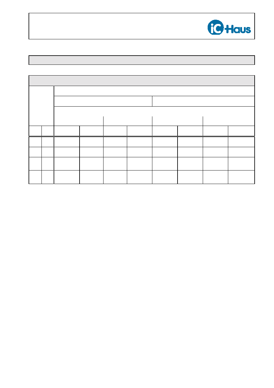
PROGRAMMING
Selection of functions
Data Word D7..D0
higher nibble
lower nibble
Selected I/O Stage function:
Address
Input
Output
Input
Output
A1
A0
Write
Read
Write
Read
Write
Read
Write
Read
0
0
Test Pattern
IR Inputs
Outputs
Outputs
Test Pattern
IR Inputs
Outputs
Outputs
0
1
IR Enable
IR Enable
Pulse Enable Pulse Enable IR Enable
IR Enable
Pulse Enable Pulse Enable
1
0
Control
Word 2
Inputs
Control
Word 2
Feedback
I/O Stages
Control
Word 2
Inputs
Control
Word 2
Feedback
I/O Stages
1
1
Control
Word 1
Control
Word 1
Control
Word 1
Control
Word 1
Control
Word 1
Control
Word 1
Control
Word 1
Control
Word 1
Reading the inputs or the output feedback (IO7..0 to D7..0)
I/O stage with input function: A high level at IOx generates a high signal at Dx (selection of functions:
read inputs) during the course of the digital hysteresis.
I/O stage with output function: A high level at IOx generates a low signal at Dx (selection of functions:
read feedback of the outputs).
The inversion while reading back the outputs (I/O stage with output function) occurs so that the same signal is
applied to Dx as was programmed for switching the output stage on or off, for example: switching on the final
stage with Dx = high results in low level at IOx. After the digital hysteresis ends, Q becomes low, the
microprocessor interface inverts this message and a high signal can be read back via Dx. The microprocessor
can check the output state in this manner.
Test
The test circuit consists of registers which can be set via the microprocessor interface (test pattern). Its content
is applied via constantly active OR gates to the counting direction inputs UP/DOWN (D7..0 to UP/DOWN7..0).
In response to a reset (low signal at RESN) the registers are set to low; as a result, there is no effect on the
UP/DOWN inputs.
In the test mode (control word 2, bit 2 and 6 at high) the comparators of the I/O stages are switched off and only
the test registers continue to operate the UP/DOWN inputs. Any desired input signals can be entered to test all
digital functions; the microprocessor can also conduct a system test in this manner.
Interrupt enable
The interrupt generation can be activated separately for every I/O stage with input function. The interrupt enable
is programmed via the data word DO..7 (function selection IR enable: 1 = stage relevant, 0 = stage not relevant).
If a signal change is recognized for an I/O stage with input function - after the digital hysteresis due to change
at Qx - and if this stage is enabled for interrupt generation, this is indicated with INTN = low. The interrupt
message as well as the interrupt register which shows the stages with signal changes are reset via control word
2 (writing bit 0 = 1 is sufficient; bit 0 = 0 is set by the chip automatically).
iC-VR
BIDIRECTIONAL µP INTERFACE TO 24V
Rev A1, Page 5/12
Signal changes which would be relevant for an interrupt generation could occur in the read-out phase following
an interrupt message. These signal changes are lost when the interrupt register is deleted. As an alternative, the
read-out of the interrupt register is possible (functional selection: read IR inputs). The registers can then be reset
separately by blocking the IR enable for each reporting stage singly and then releasing it (functional selection:
IR enable).
Filter periods
The input comparator of each I/O stage switches the counting direction of a 3 bit counter. The counter output Q
does not change until the final status is reached (to high for high level at IOx, to low for low level at IOx if
constantly applied during the filter period).
The counter is clocked externally (pin CLK); the divisor for the clock frequency can be programmed separately
for both nibbles. A low signal at reset input RESN resets the counters to the value 3. Due to the digital hysteresis,
the change of an input signal is therefore not recognized until the selected filter period has elapsed.
Pulse enable and pulse times
The flashing or pulsing function can be switched on separately for each I/O stage with output function. The
programming of the divisors for the flashing frequency input BLFQ (control word 1, bits 0,1 and 4,5) is conducted
for each nibble. The clock signal at BLFQ is transfered with the slope of CLK (synchronized). For this reason the
clock frequency for CLK must be higher than the clock frequency for BLFQ, e. g. 2 MHz for CLK and 50 Hz for
BLFQ.
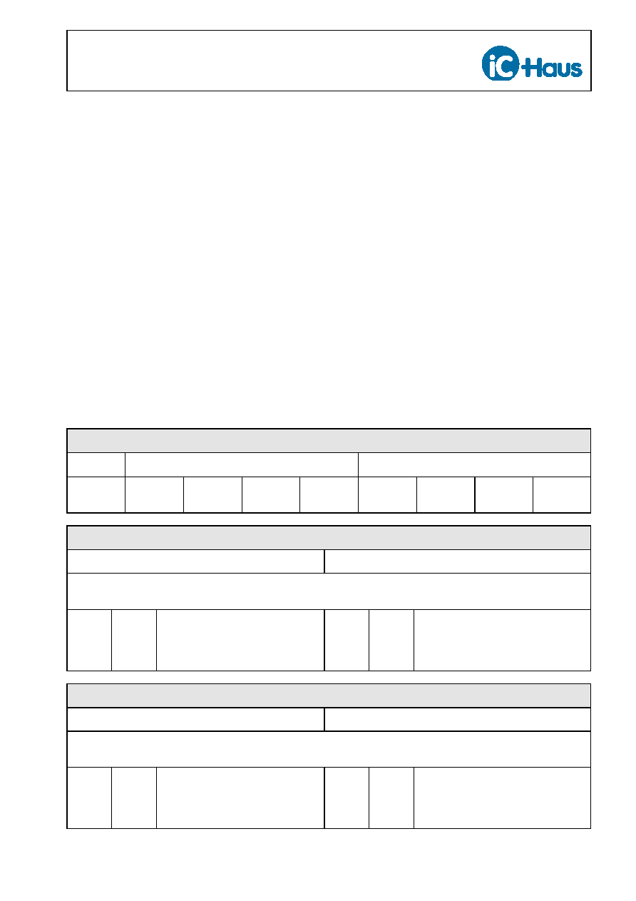
Control Word 1
higher nibble
lower nibble
Bit
Name
7
FH0
6
FH1
5
PH0
4
PH1
3
FL0
2
FL1
1
PL0
0
PL1
Control Word 1 (lower nibble)
Filtering Time
Flashing Pulse Duration
Bit 3
FLO
Bit 2
FL1
Bit 1
PLO
Bit 0
PL1
0
1
0
1
0
0
1
1
14.5 * CLK
± 1 * CLK
896.5 * CLK
± 64 * CLK
3584.5 * CLK
± 256 * CLK
7168.5 * CLK
± 512 * CLK
0
1
0
1
0
0
1
1
BLFQ
BLFQ * 2
BLFQ * 4
BLFQ * 16
Control Word 1 (higher nibble)
Filtering Time
Flashing Pulse Duration
Bit 7
FHO
Bit 6
FH1
Bit 5
PHO
Bit 4
PH1
0
1
0
1
0
0
1
1
14.5 * CLK
± 1 * CLK
896.5 * CLK
± 64 * CLK
3584.5 * CLK
± 256 * CLK
7168.5 * CLK
± 512 * CLK
0
1
0
1
0
0
1
1
BLFQ
BLFQ * 2
BLFQ * 4
BLFQ * 16