YDA135
D-20
STEREO 5W-20W DIGITAL AUDIO POWER AMPLIFIER CONTROLLER
YDA135 is digital audio power amplifier controller IC that is output power of 20W/channel on a 12V power supply
operation.
This IC is combined with the general purpose Power MOSFET (hereafter called Power MOSFET) that are
connected through BTL can configure an audio power amplifier with output power of 5W or 20W.
This IC accepts analog signal, converts it into digital pulse signal by the digital modulation circuitry and outputs
the digital pulse signal for driving Power MOSFET. The Power MOSFET that is driven by this IC outputs large
current digital pulses. The digital pulse signal is converted to audio signal through an external low pass filter, and
sent to the speakers.
By using a general purpose Power MOSFET, very low cost digital amplifier system is configured. By adapting
Yamaha's proprietary modulation system, the device provides low distortion and high signal to noise ratio at the
highest level among digital amplifiers in the equiralent class.
This IC has the overcurrent detection function that detects overcurrent state by voltage drop of external resistors
that detects the output current.
This IC has the high temperature detection function that detects high temperature by resistor value change of
external element that detects temperature.
The operation of this IC is limited by using two control signal, SLEEP or MUTE. SLEEP signal stops all functions
of this IC, and restrain to the power consumption at the minimum. MUTE signal brings Power MOSFET into
nonconductive state, and mute the output of the device.
This IC is configured by two power supply ; 5V for signal processing circuits, and 12V for Power MOSFET driving
circuits.
YDA135CATALOG
CATALOG No.:LSI-4DA135A2
2003.3
CS(Channel
separation)
80
dB
1kHz
Any
gain
setting
by
external
resistors
Sleep
function
by
SLEEP
terminal
Output
mute
function
by
MUTE
terminal
Over
current
detection
function
(Power
supply
short-circuiting,
Ground
short-
circuiting,
Load
short-circuiting)
High
temperature
detection
function
Pop
noise
suppression
function
at
turn-on
and
turn-off
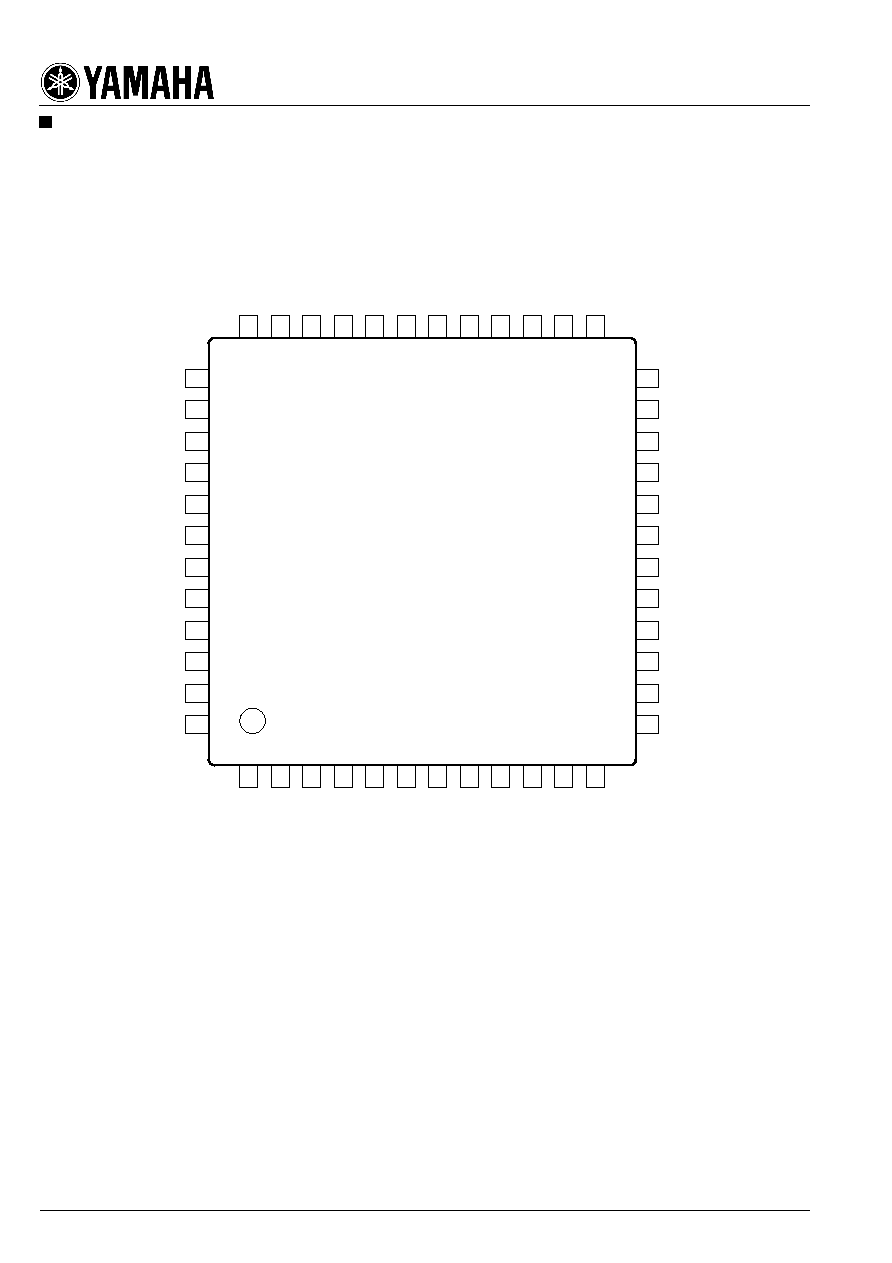
48-pin
plastic
LQFP
(YDA135-VZ)
High
output
power
20W
V
DDP
=12.0V
R
L
=4
THD+N<10%
High
efficiency
operation
80
%
V
DDP
=12.0V
R
L
=4
Po=20W
85
%
V
DDP
=12.0V
R
L
=8
Po=10W
Low
distortion(THD+N)
0.03
%
1kHz
R
L
=4
Po=7W
High
signal
to
noise
ratio
100
dB
V
DDP
=12.0V
Input
sensitivity1.0V
R
L
=4
97
dB
V
DDP
=12.0V
Input
sensitivity150mV
R
L
=4
Low
consumption
current
(12V/5V
power
supply)
When
Power
MOSFET
(FW332)
is
connected.
30mA
/7mA
V
DDP
=12.0V
no
signal
0.1mA/7mA
V
DDP
=12.0V
at
mute
1A/1A
V
DDP
=12.0V
at
sleep
Outline
Features

YDA135
3
No.
Name
Function
1
2
3
4
6
7
8
9
10
11
12
13
14
15
16
17
18
19
20
21
22
23
24
N/C
VREFL
VSSL
MUTE
PROT
N/C
TPP
TEST
VSSR
VREFR
N/C
VDDR
INR
NFINR
NFPR
NFNR
N/C
CDOR
CDIR
N/C
SENSEPR
PVDDR
SENSENR
L
channel
reference
voltage
output
Warning
signal
output
for
detection
function
Ground
for
5V
power
supply
of
L
channel
High
temperature
detection
Non
connection
5V
Power
supply
of
R
channel
R
channel
analog
signal
input
R
channel
input
gain
setting
R
channel
positive
side
feedback
input
R
channel
negative
side
feedback
input
Non
connection
R
channel
off
time
setting
(output)
R
channel
off
time
setting
(input)
Non
connection
R
channel
overcurrent
detection
(PVDD
side)
12V
power
supply
of
R
channel
R
channel
overcurrent
detection
(PVSS
side)
Non
connection
Mute
control
Non
connection
IC
test.
Connect
to
VSSR
Ground
for
5V
power
supply
of
R
channel
R
channel
reference
voltage
output
5
SLEEP
Sleep
control
I/O
I
I
O
O
O
I
I
-
-
-
-
I
O
I
-
O
-
I
I
IH
-
IH
-
-
Note.
I/O:
5V
input/
5V
output,
IH/OH:
12V
input/12V
output
25
26
27
28
30
31
32
33
34
35
36
37
38
39
40
41
42
43
44
45
46
47
48
PVSSR
N/C
HP_R
HN_R
LP_R
LP_L
LN_L
HN_L
HP_L
N/C
PVSSL
SENSENL
PVDDL
SENSEPL
N/C
CDIL
CDOL
N/C
NFNL
NFPL
NFINL
INL
VDDL
Non
connection
R
channel
negative
side
PMOS
driving
R
channel
positive
side
PMOS
driving
L
channel
negative
side
NMOS
driving
Ground
for
12V
power
supply
of
L
channel
L
channel
overcurrent
detection
(PVSS
side)
12V
power
supply
of
L
channel
L
channel
overcurrent
detection
(PVDD
side)
Non
connection
L
channel
off
time
setting
(input)
L
channel
off
time
setting
(output)
Non
connection
L
channel
negative
side
feedback
input
L
channel
positive
side
feedback
input
L
channel
input
gain
setting
L
channel
analog
signal
input
5V
power
supply
of
L
channel
Ground
for
12V
power
supply
of
R
channel
R
channel
positive
side
NMOS
driving
L
channel
negative
side
PMOS
driving
L
channel
positive
side
NMOS
driving
L
channel
positive
side
PMOS
driving
Non
connection
29
LN_R
R
channel
negative
side
NMOS
driving
OH
OH
OH
-
-
OH
OH
OH
OH
OH
IH
-
IH
-
O
-
I
I
I
O
I
-
-
-
Terminal function

YDA135
5
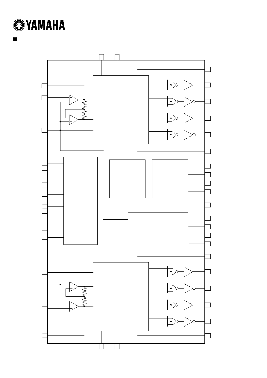
VDDL, VSSL, VDDR, VSSR (Pin No.48, 3, 13, 10)
VDDL and VSSL terminals are 5.0V power supply terminal and ground terminal for left channel signal processing
circuit respectively. VDDR and VSSR terminals are 5.0V power supply terminal and ground terminal for right
channel signal processing circuit respectively.
Left and right channels are equipped independent power supply terminal and ground terminal, respectirely.
All the ground terminals are connected through IC board (low resistor), but the power supply terminals for left and
right channels are separated from each other.
PVDDL, PVSSL, PVDDR, PVSSR (Pin No.38, 36, 23, 25)
PVDDL and PVSSL are 12 V power supply and ground terminals for left channel Power MOSFET driving circuit
respectively.
PVDDR and PVSSR are 12 V power supply and ground terminals for right channel Power MOSFET driving circuit
respectively.
Left and right channels are equipped independent power supply terminal and ground terminal, respectirely.
All the ground terminals are connected through IC board (low resistor), but the power supply terminals for left and
right channels are separated from each other.
In the following explanations, "L" level and "H" level of SLEEP and MUTE terminals mean "V
IL
" and "V
IH
"
respectively, and "L" level and "H" level of PROT terminal mean "V
OL
" and "V
OH
" respectively.
"L" level and "H" level of output terminals such as HP_L and HN_L terminals also mean "V
HOL
" and "V
HOH
"
respectively.
Description of terminal function
Power supply and ground terminals
INL, NFINL, INR, NFINR (Pin No.47, 46, 14, 15)
INL and NFINL are analog signal input and gain adjustment terminals for left channel.
INR and NFINR are analog signal input and gain adjustment terminals for right channel.
The terminals are connected respectively to the negative input terminal and output terminal of the first stage
inversion operational amplifiers.
The amplifier gain is set by connecting an input resistor and a feedback resistor to both terminals as shown the
"Example of application circuit".
The use of this inversion operational amplifier allows making a filter such as low band boost filter.
VREFL, VREFR (Pin No.2, 11)
VREFL is the reference voltage output terminal for the left channel. It outputs 1/2 of 5V power supply terminal
(VDDL) voltage.
VREFR is the reference voltage output terminal for the right channel. It outputs 1/2 of 5V power supply terminal
(VDDR) voltage.
Connect a capacitor with capacitance necessary to stabilize the voltage. Refer to "Pop noise reduction functions".
NFPL, NFNL, NFPR, NFNR (Pin No.45, 44, 16, 17)
NFPL and NFNL are the digital amplifier feedback input terminals for left channel.
NFPR and NFNR are the digital amplifier feedback input terminals for right channel.
Connect the feedback signal of positive side and negative side of H-bridge configuration Power MOSFET output to
each terminal. At this time, as described in the "Example of application circuit", divide the voltage of feedback signal
with external resistor to prevent the maximum voltage from exceeding 5V and input to each terminal.
HP_L, HN_L, LP_L, LN_L, HP_R, HN_R, LP_R, LN_R (Pin No.34, 33, 31, 32, 27, 28, 30, 29)
HP_L, HN_L, LP_L and LN_L are Power MOSFET driving terminals for left channel.
HP_L is a driving output terminal for positive side P channel Power MOSFET (PMOS), HN_L is the one for positive
side N channel Power MOSFET (NMOS), LP_L is the one for negative side P channel Power MOSFET (PMOS),
and LN_L is the one for negative side N channel Power MOSFET (NMOS).
HP_R, HN_R, LP_R and LN_R are Power MOSFET driving terminals for right channel.
HP_R is a driving output terminal for positive side P channel Power MOSFET (PMOS), HN_R is the one for positive
side N channel Power MOSFET (NMOS), LP_R is the one for negative side P channel Power MOSFET (PMOS),
and LN_R is the one for negative side N channel Power MOSFET (NMOS).
Analog terminals