"8-Bit Registers"
CY54FCT273T, CY74FCT273T
8-BIT REGISTERS
SCCS020A MARCH 1995 REVISED OCTOBER 2001
1
POST OFFICE BOX 655303
·
DALLAS, TEXAS 75265
D
Function, Pinout, and Drive Compatible
With FCT and F Logic
D
Reduced V
OH
(Typically = 3.3 V) Versions
of Equivalent FCT Functions
D
Edge-Rate Control Circuitry for
Significantly Improved Noise
Characteristics
D
I
off
Supports Partial-Power-Down Mode
Operation
D
Matched Rise and Fall Times
D
ESD Protection Exceeds JESD 22
2000-V Human-Body Model (A114-A)
200-V Machine Model (A115-A)
1000-V Charged-Device Model (C101)
D
Fully Compatible With TTL Input and
Output Logic Levels
D
CY54FCT273T
32-mA Output Sink Current
12-mA Output Source Current
D
CY74FCT273T
64-mA Output Sink Current
32-mA Output Source Current
description
The 'FCT273T devices consist of eight
edge-triggered D-type flip-flops with individual
D
inputs and Q outputs. The common
buffered-clock (CP) and master-reset (MR) inputs
load and reset all flip-flops simultaneously. These
devices are edge-triggered registers. The state of
each D input (one setup time before the
low-to-high clock transition) is transferred to the
corresponding flip-flop's Q output. All outputs are
forced low by a low logic level on the MR input.
This device is fully specified for
partial-power-down applications using I
off
. The I
off
circuitry disables the outputs, preventing
damaging current backflow through the device
when it is powered down.
Copyright
2001, Texas Instruments Incorporated
PRODUCTION DATA information is current as of publication date.
Products conform to specifications per the terms of Texas Instruments
standard warranty. Production processing does not necessarily include
testing of all parameters.
Please be aware that an important notice concerning availability, standard warranty, and use in critical applications of
Texas Instruments semiconductor products and disclaimers thereto appears at the end of this data sheet.
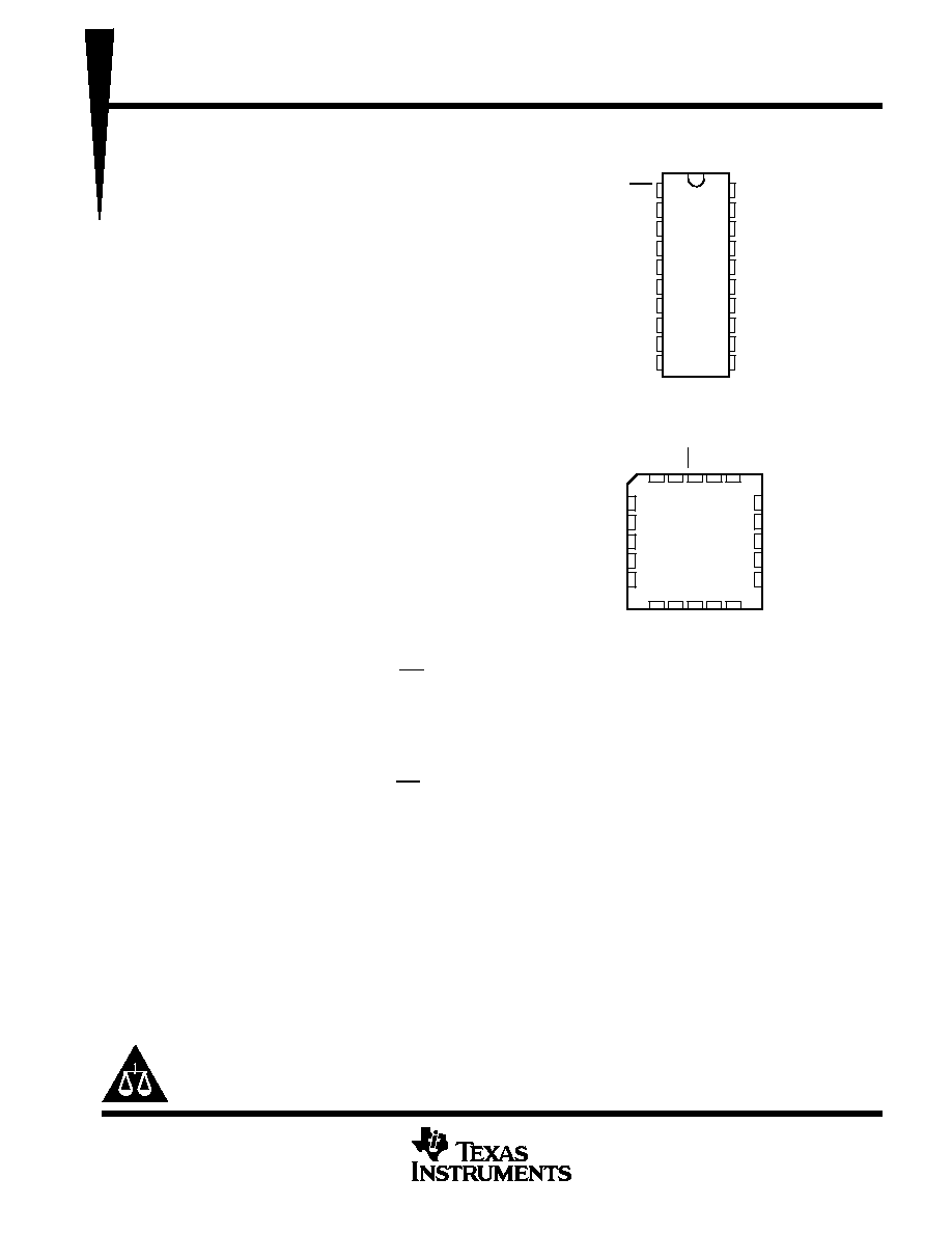
CY54FCT273T . . . D PACKAGE
CY74FCT273T . . . Q OR SO PACKAGE
(TOP VIEW)
CY54FCT273T . . . L PACKAGE
(TOP VIEW)
1
2
3
4
5
6
7
8
9
10
20
19
18
17
16
15
14
13
12
11
MR
Q
0
D
0
D
1
Q
1
Q
2
D
2
D
3
Q
3
GND
V
CC
Q
7
D
7
D
6
Q
6
Q
5
D
5
D
4
Q
4
CP
3
2
1 20 19
9 10 11 12 13
4
5
6
7
8
18
17
16
15
14
D
1
Q
1
Q
2
D
2
D
3
D
MR
3
GND
V
CC
D
7
D
6
Q
6
Q
5
D
5
Q
CP
4
Q
4
D
0
Q
0
Q
7
CY54FCT273T, CY74FCT273T
8-BIT REGISTERS
SCCS020A MARCH 1995 REVISED OCTOBER 2001
2
POST OFFICE BOX 655303
·
DALLAS, TEXAS 75265
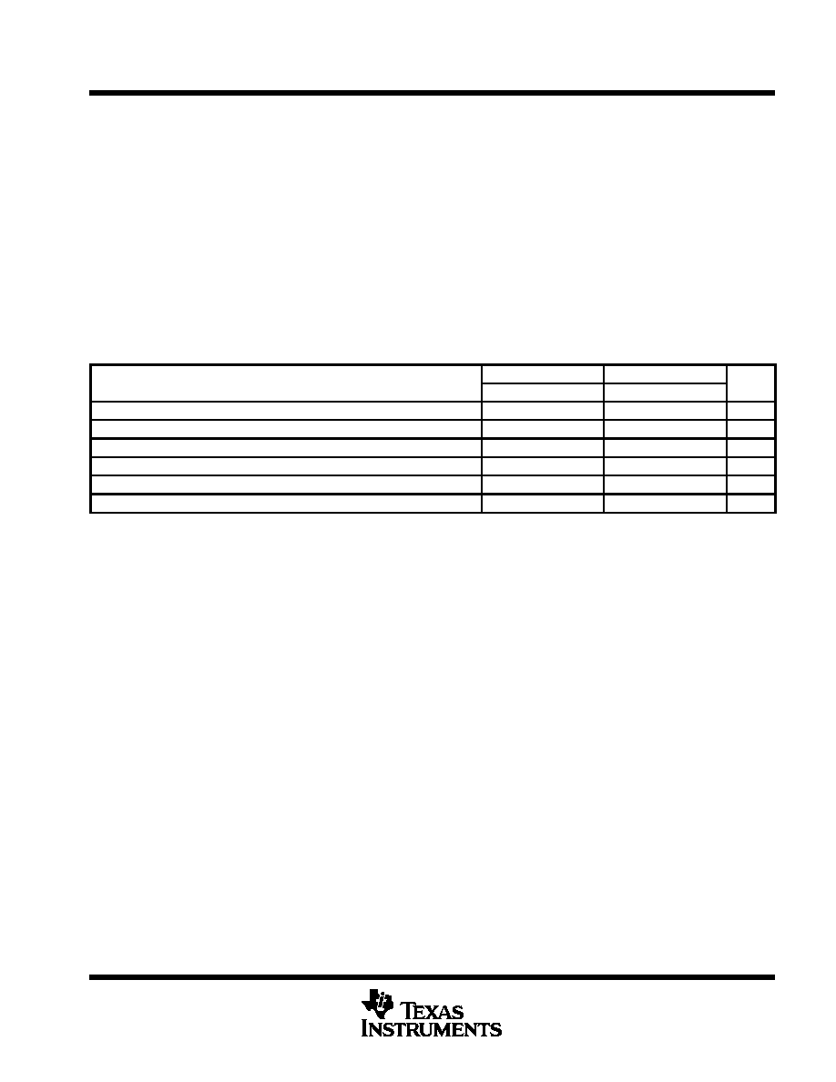
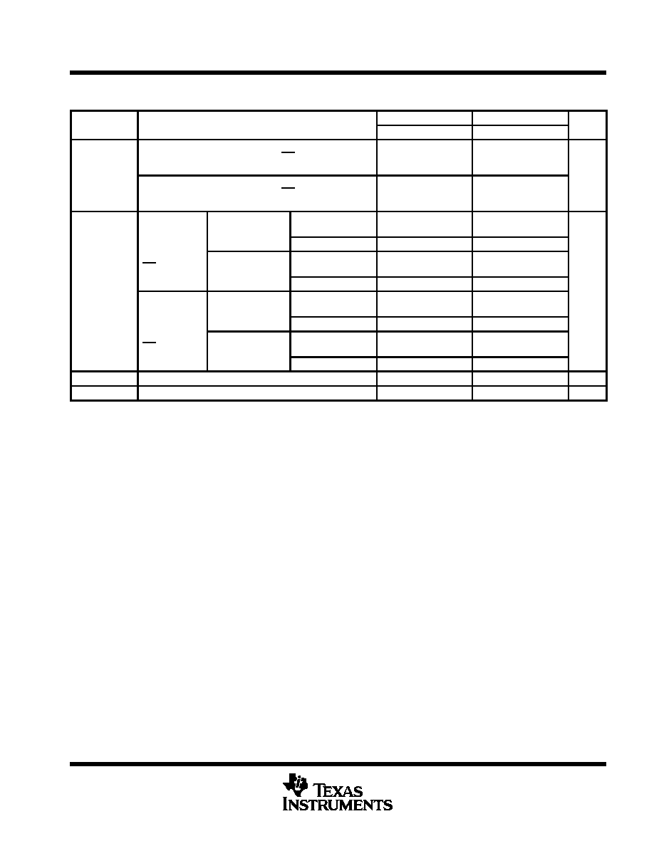
ORDERING INFORMATION
TA
PACKAGE
SPEED
(ns)
ORDERABLE
PART NUMBER
TOP-SIDE
MARKING
QSOP Q
Tape and reel
5.8
CY74FCT273CTQCT
FCT273C
SOIC
SO
Tube
5.8
CY74FCT273CTSOC
FCT273C
SOIC SO
Tape and reel
5.8
CY74FCT273CTSOCT
FCT273C
QSOP Q
Tape and reel
7.2
CY74FCT273ATQCT
FCT273A
40
°
C to 85
°
C
SOIC
SO
Tube
7.2
CY74FCT273ATSOC
FCT273A
SOIC SO
Tape and reel
7.2
CY74FCT273ATSOCT
FCT273A
QSOP Q
Tape and reel
13
CY74FCT273TQCT
FCT273
SOIC
SO
Tube
13
CY74FCT273TSOC
FCT273
SOIC SO
Tape and reel
13
CY74FCT273TSOCT
FCT273
55
°
C to 125
°
C
LCC L
Tube
8.3
CY54FCT273ATLMB
Package drawings, standard packing quantities, thermal data, symbolization, and PCB design guidelines are
available at www.ti.com/sc/package.
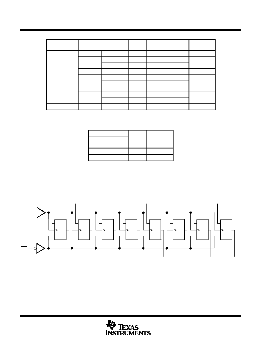
FUNCTION TABLE
INPUTS
OUTPUT
OPERATING
MR
CP
D
Q
MODE
L
X
X
L
Reset (clear)
H
h
H
Load `1'
H
l
L
Load `0'
H = High logic level steady state, h = High logic level one
setup time prior to low-to-high clock transition, L = Low
logic level steady state, l = Low logic level one setup time
prior to the low-to-high transition, X = Don't care,
= Low-to-high clock transition
logic diagram (positive logic)
CP
D0
MR
1D
R
C1
1D
R
C1
1D
R
C1
1D
R
C1
1D
R
C1
1D
R
C1
1D
R
C1
1D
R
C1
3
4
7
8
13
14
17
18
2
5
6
9
12
15
16
19
11
1
D1
D2
D3
D4
D5
D6
D7
Q0
Q1
Q2
Q3
Q4
Q5
Q6
Q7
CY54FCT273T, CY74FCT273T
8-BIT REGISTERS
SCCS020A MARCH 1995 REVISED OCTOBER 2001
3
POST OFFICE BOX 655303
·
DALLAS, TEXAS 75265
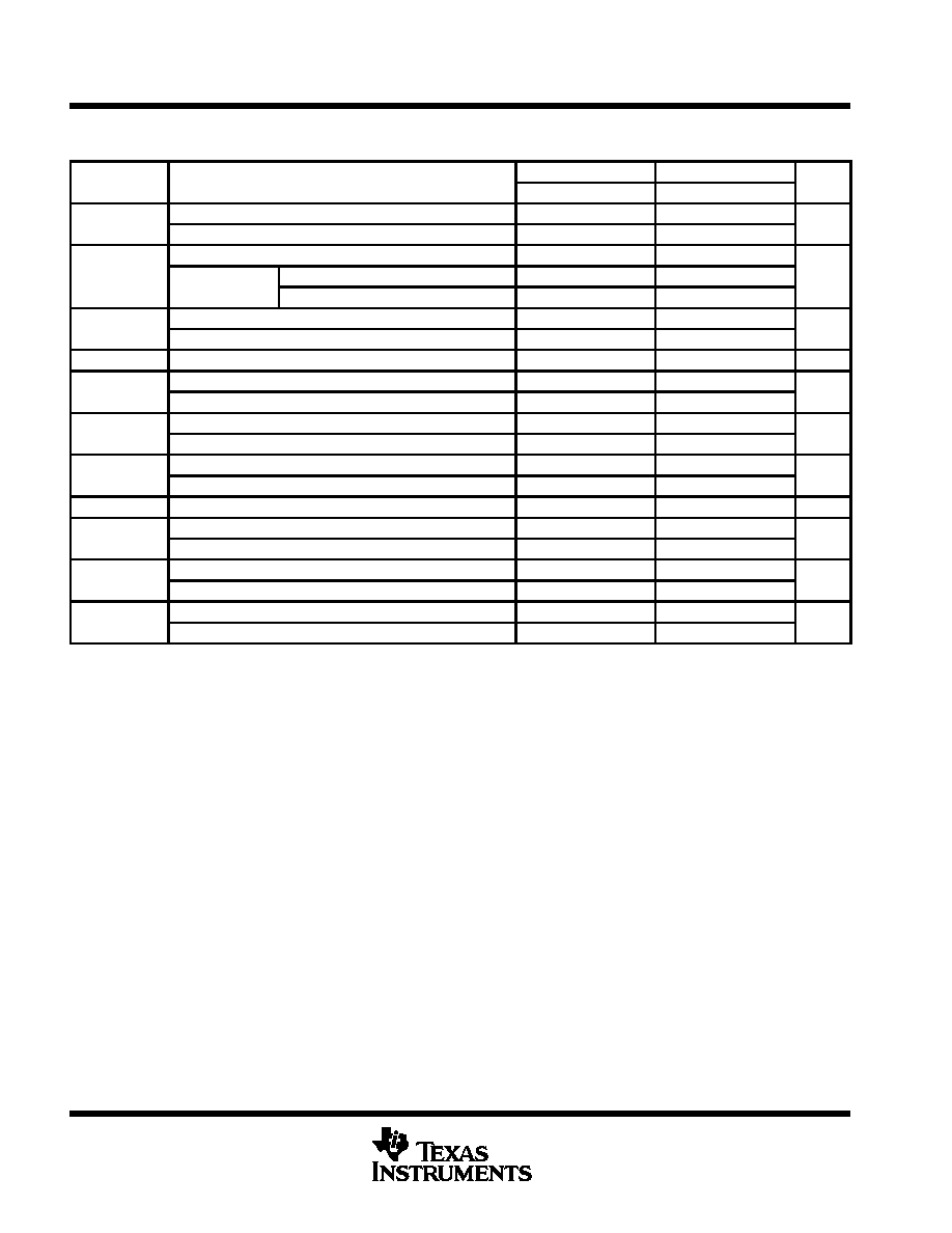
absolute maximum ratings over operating free-air temperature range (unless otherwise noted)
Supply voltage range to ground potential
0.5 V to 7 V
. . . . . . . . . . . . . . . . . . . . . . . . . . . . . . . . . . . . . . . . . . . . . .
DC input voltage range
0.5 V to 7 V
. . . . . . . . . . . . . . . . . . . . . . . . . . . . . . . . . . . . . . . . . . . . . . . . . . . . . . . . . . . . .
DC output voltage range
0.5 V to 7 V
. . . . . . . . . . . . . . . . . . . . . . . . . . . . . . . . . . . . . . . . . . . . . . . . . . . . . . . . . . . .
DC output current (maximum sink current/pin)
120 mA
. . . . . . . . . . . . . . . . . . . . . . . . . . . . . . . . . . . . . . . . . . . . . .
Package thermal impedance,
JA
(see Note 1): Q package
68
°
C/W
. . . . . . . . . . . . . . . . . . . . . . . . . . . . . . . . . .
SO package
58
°
C/W
. . . . . . . . . . . . . . . . . . . . . . . . . . . . . . . . .
Ambient temperature range with power applied, T
A
65
°
C to 135
°
C
. . . . . . . . . . . . . . . . . . . . . . . . . . . . . . . . . . .
Storage temperature range, T
stg
65
°
C to 150
°
C
. . . . . . . . . . . . . . . . . . . . . . . . . . . . . . . . . . . . . . . . . . . . . . . . . . .
Stresses beyond those listed under "absolute maximum ratings" may cause permanent damage to the device. These are stress ratings only, and
functional operation of the device at these or any other conditions beyond those indicated under "recommended operating conditions" is not implied.
Exposure to absolute-maximum-rated conditions for extended periods may affect device reliability.
NOTE 1: The package thermal impedance is calculated in accordance with JESD 51-7.
recommended operating conditions (see Note 2)
CY54FCT273T
CY74FCT273T
UNIT
MIN
NOM
MAX
MIN
NOM
MAX
UNIT
VCC
Supply voltage
4.5
5
5.5
4.75
5
5.25
V
VIH
High-level input voltage
2
2
V
VIL
Low-level input voltage
0.8
0.8
V
IOH
High-level output current
12
32
mA
IOL
Low-level output current
32
64
mA
TA
Operating free-air temperature
55
125
40
85
°
C
NOTE 2: All unused inputs of the device must be held at VCC or GND to ensure proper device operation.
CY54FCT273T, CY74FCT273T
8-BIT REGISTERS
SCCS020A MARCH 1995 REVISED OCTOBER 2001
4
POST OFFICE BOX 655303
·
DALLAS, TEXAS 75265
electrical characteristics over recommended operating free-air temperature range (unless
otherwise noted)
PARAMETER
TEST CONDITIONS
CY54FCT273T
CY74FCT273T
UNIT
PARAMETER
TEST CONDITIONS
MIN
TYP
MAX
MIN
TYP
MAX
UNIT
VIK
VCC = 4.5 V,
IIN = 18 mA
0.7
1.2
V
VIK
VCC = 4.75 V,
IIN = 18 mA
0.7
1.2
V
VCC = 4.5 V,
IOH = 12 mA
2.4
3.3
VOH
VCC 4 75 V
IOH = 32 mA
2
V
VCC = 4.75 V
IOH = 15 mA
2.4
3.3
VOL
VCC = 4.5 V,
IOL = 32 mA
0.3
0.55
V
VOL
VCC = 4.75 V,
IOL = 64 mA
0.3
0.55
V
Vhys
All inputs
0.2
0.2
V
II
VCC = 5.5 V,
VIN = VCC
5
µ
A
II
VCC = 5.25 V,
VIN = VCC
5
µ
A
IIH
VCC = 5.5 V,
VIN = 2.7 V
±
1
µ
A
IIH
VCC = 5.25 V,
VIN = 2.7 V
±
1
µ
A
IIL
VCC = 5.5 V,
VIN = 0.5 V
±
1
µ
A
IIL
VCC = 5.25 V,
VIN = 0.5 V
±
1
µ
A
Ioff
VCC = 0 V,
VOUT = 4.5 V
±
1
±
1
µ
A
IOS
VCC = 5.5 V,
VOUT = 0 V
60
120
225
mA
IOS
VCC = 5.25 V,
VOUT = 0 V
60
120
225
mA
ICC
VCC = 5.5 V,
VIN
0.2 V,
VIN
VCC 0.2 V
0.1
0.2
mA
ICC
VCC = 5.25 V,
VIN
0.2 V,
VIN
VCC 0.2 V
0.1
0.2
mA
ICC
VCC = 5.5 V, VIN = 3.4 V§, f1 = 0, Outputs open
0.5
2
mA
ICC
VCC = 5.25 V, VIN = 3.4 V§, f1 = 0, Outputs open
0.5
2
mA
Typical values are at VCC = 5 V, TA = 25
°
C.
Not more than one output should be shorted at a time. Duration of short should not exceed one second. The use of high-speed test apparatus and/or
sample-and-hold techniques are preferable to minimize internal chip heating and more accurately reflect operational values. Otherwise, prolonged
shorting of a high output can raise the chip temperature well above normal and cause invalid readings in other parametric tests. In any sequence
of parameter tests, IOS tests should be performed last.
§ Per TTL-driven input (VIN = 3.4 V); all other inputs at VCC or GND
CY54FCT273T, CY74FCT273T
8-BIT REGISTERS
SCCS020A MARCH 1995 REVISED OCTOBER 2001
5
POST OFFICE BOX 655303
·
DALLAS, TEXAS 75265
electrical characteristics over recommended operating free-air temperature range (unless
otherwise noted) (continued)
PARAMETER
TEST CONDITIONS
CY54FCT273T
CY74FCT273T
UNIT
PARAMETER
TEST CONDITIONS
MIN
TYP
MAX
MIN
TYP
MAX
UNIT
ICCD¶
VCC = 5.5 V, Outputs open,
One bit switching at 50% duty cycle, MR = VCC,
VIN
0.2 V or VIN
VCC 0.2 V
0.06
0.12
mA/
ICCD¶
VCC = 5.25 V, Outputs open,
One bit switching at 50% duty cycle, MR = VCC,
VIN
0.2 V or VIN
VCC 0.2 V
0.06
0.12
MHz
#
VCC = 5 5 V
One bit switching
at f1 = 2.5 MHz
VIN
0.2 V or
VIN
VCC 0.2 V
0.7
1.4
#
VCC = 5.5 V,
f0 = 10 MHz,
1
at 50% duty cycle
VIN = 3.4 V or GND
1.2
3.4
#
0
,
Outputs open,
MR = VCC
Eight bits switching
at f1 = 2.5 MHz
VIN
0.2 V or
VIN
VCC 0.2 V
1.6
3.2||
IC#
1
at 50% duty cycle
VIN = 3.4 V or GND
3.9
12.2||
mA
IC#
VCC = 5 25 V
One bit switching
at f1 = 5 MHz
VIN
0.2 V or
VIN
VCC 0.2 V
0.7
1.4
mA
VCC = 5.25 V,
f0 = 10 MHz,
1
at 50% duty cycle
VIN = 3.4 V or GND
1.2
3.4
0
,
Outputs open,
MR = VCC
Eight bits switching
at f1 = 5 MHz
VIN
0.2 V or
VIN
VCC 0.2 V
1.6
3.2||
1
at 50% duty cycle
VIN = 3.4 V or GND
3.9
12.2||
Ci
5
10
5
10
pF
Co
9
12
9
12
pF
Typical values are at VCC = 5 V, TA = 25
°
C.
¶ This parameter is derived for use in total power-supply calculations.
# IC
= ICC +
ICC
×
DH
×
NT + ICCD (f0/2 + f1
×
N1)
Where:
IC
= Total supply current
ICC
= Power-supply current with CMOS input levels
ICC = Power-supply current for a TTL high input (VIN = 3.4 V)
DH
= Duty cycle for TTL inputs high
NT
= Number of TTL inputs at DH
ICCD = Dynamic current caused by an input transition pair (HLH or LHL)
f0
= Clock frequency for registered devices, otherwise zero
f1
= Input signal frequency
N1
= Number of inputs changing at f1
All currents are in milliamperes and all frequencies are in megahertz.
|| Values for these conditions are examples of the ICC formula.