
1/10
May 2002
s
HIGH SPEED: t
PD
= 3.0ns (TYP.) at V
CC
= 5V
s
LOW POWER DISSIPATION:
I
CC
= 1
µ
A(MAX.) at T
A
=25∞C
s
TYPICAL HYSTERESIS:
V
H
= 800mV
at V
CC
= 4.5V
V
H
= 500mV
at V
CC
= 3.0V
s
POWER DOWN PROTECTION ON INPUTS
AND OUTPUTS
s
SYMMETRICAL OUTPUT IMPEDANCE:
|I
OH
| = I
OL
= 8mA (MIN) at V
CC
= 4.5V
II
OH
| = I
OL
= 4mA (MIN) at V
CC
= 3.0V
s
BALANCED PROPAGATION DELAYS:
t
PLH
t
PHL
s
OPERATING VOLTAGE RANGE:
V
CC
(OPR) = 2V to 5.5V
s
IMPROVED LATCH-UP IMMUNITY
DESCRIPTION
The 74V2G14 is an advanced high-speed CMOS
TRIPLE SCHMITT TRIGGER INVERTER
fabricated with sub-micron silicon gate and
double-layer metal wiring C
2
MOS tecnology.
The internal circuit is composed of 3 stages
including buffer output, which provide high noise
immunity and stable output.
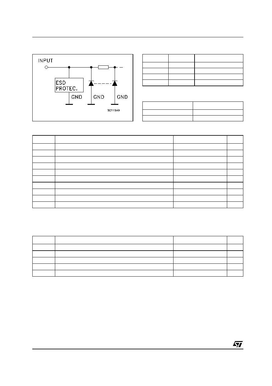
Power down protection is provided on all inputs
and outputs and 0 to 7V can be accepted on
inputs with no regard to the supply voltage.
Pin configuration and function are the same as
those of the 74V2G04, but 74V2G14 has
hysteresis on inputs.
This device can be used to interface 5V to 3V
systems and it is ideal for portable applications
like personal digital assistant, camcorder and all
battery-powered equipment.
All inputs and outputs are equipped with
protection circuits against static discharge, giving
them ESD immunity and transient excess voltage.
74V2G14
TRIPLE SCHMITT INVERTER
PIN CONNECTION AND IEC LOGIC SYMBOLS
ORDER CODES
PACKAGE
T & R
SOT23-8L
74V2G14STR
SOT323-8L
74V2G14CTR
SOT23-8L
SOT323-8L
74V2G14
2/10
INPUT EQUIVALENT CIRCUIT
PIN DESCRIPTION
TRUTH TABLE
ABSOLUTE MAXIMUM RATINGS
Absolute Maximum Ratings are those values beyond which damage to the device may occur. Functional operation under these conditions is
not implied.
1) Vcc=0V
2) High or Low State
RECOMMENDED OPERATING CONDITIONS
PIN No
SYMBOL
NAME QND FUNCTION
1, 3, 6
1A, 2A, 3A
Data Inputs
7, 5, 2
1Y, 2Y, 3Y
Data Outputs
4
GND
Ground (0V)
8
V
CC
Positive Supply Voltage
nA
nY
L
H
H
L
Symbol
Parameter
Value
Unit
V
CC
Supply Voltage
-0.5 to +7.0
V
V
I
DC Input Voltage
-0.5 to +7.0
V
V
O
DC Output Voltage (see note 1)
-0.5 to +7.0
V
V
O
DC Output Voltage (see note 2)
-0.5 to V
CC
+ 0.5
V
I
IK
DC Input Diode Current
-
20
mA
I
OK
DC Output Diode Current
-
20
mA
I
O
DC Output Current
±
25
mA
I
CC
or I
GND
DC V
CC
or Ground Current
±
50
mA
T
stg
Storage Temperature
-65 to +150
∞C
T
L
Lead Temperature (10 sec)
260
∞C
Symbol
Parameter
Value
Unit
V
CC
Supply Voltage
2 to 5.5
V
V
I
Input Voltage
0 to 5.5
V
V
O
Output Voltage
0 to 5.5
V
V
O
Output Voltage
0 to V
CC
V
T
op
Operating Temperature
-55 to 125
∞C
74V2G14
3/10
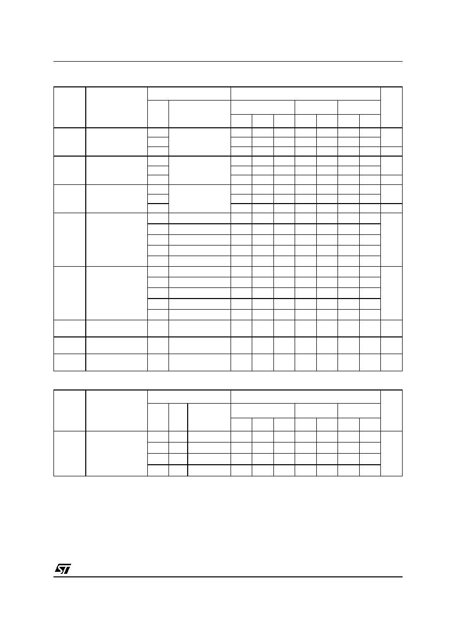
DC SPECIFICATIONS
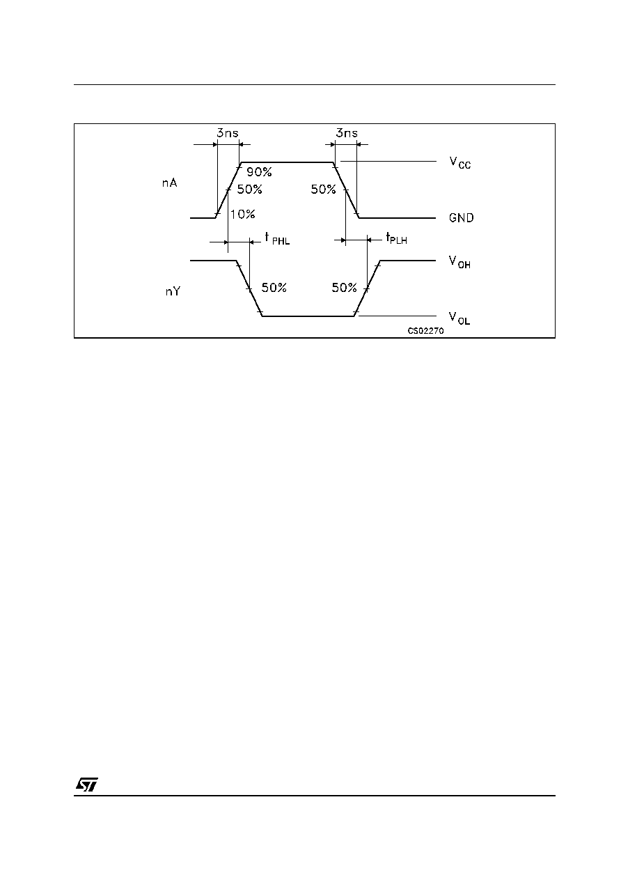
AC ELECTRICAL CHARACTERISTICS (Input t
r
= t
f
= 3ns)
(*) Voltage range is 3.3V
±
0.3V
(**) Voltage range is 5.0V
±
0.5V
Symbol
Parameter
Test Condition
Value
Unit
V
CC
(V)
T
A
= 25∞C
-40 to 85∞C
-55 to 125∞C
Min.
Typ.
Max.
Min.
Max.
Min.
Max.
V
P
High Level Input
Voltage
3.0
2.20
2.20
2.20
V
4.5
3.15
3.15
3.15
5.5
3.85
3.85
3.85
V
N
Low Level Input
Voltage
3.0
0.90
0.90
0.90
V
4.5
1.35
1.35
1.35
5.5
1.65
1.65
1.65
V
H
Hysteresis Voltage
3.0
0.30
1.20
0.30
1.20
0.30
1.20
V
4.5
0.40
1.40
0.40
1.40
0.40
1.40
5.5
0.50
1.60
0.50
1.60
0.50
1.60
V
OH
High Level Ouput
Voltage
2.0
I
O
=-50
µ
A
1.9
2.0
1.9
1.9
V
3.0
I
O
=-50
µ
A
2.9
3.0
2.9
2.9
4.5
I
O
=-50
µ
A
4.4
4.5
4.4
4.4
3.0
I
O
=-4 mA
2.58
2.48
2.4
4.5
I
O
=-8 mA
3.94
3.8
3.7
V
OL
Low Level Output
Voltage
2.0
I
O
=50
µ
A
0.0
0.1
0.1
0.1
V
3.0
I
O
=50
µ
A
0.0
0.1
0.1
0.1
4.5
I
O
=50
µ
A
0.0
0.1
0.1
0.1
3.0
I
O
=4 mA
0.36
0.44
0.55
4.5
I
O
=8 mA
0.36
0.44
0.55
I
I
Input Leakage
Current
0 to
5.5
V
I
= 5.5V or GND
±
0.1
±
1
±
1
µ
A
I
CC
Quiescent Supply
Current
5.5
V
I
= V
CC
or GND
1
10
20
µ
A
I
OPD
Power down Output
Leakage Current
0
V
O
= 5.5
0.5
5
10
µ
A
Symbol
Parameter
Test Condition
Value
Unit
V
CC
(V)
C
L
(pF)
T
A
= 25∞C
-40 to 85∞C
-55 to 125∞C
Min.
Typ.
Max.
Min.
Max.
Min.
Max.
t
PLH
t
PHL
Propagation Delay
Time
3.3
(*)
15
3.7
7.0
1.0
8.0
1.0
9.0
ns
3.3
(*)
50
5.3
8.0
1.0
9.5
1.0
10.5
5.0
(**)
15
3.0
5.0
1.0
6.0
1.0
7.0
5.0
(**)
50
4.1
6.5
1.0
7.5
1.0
8.5

74V2G14
4/10
CAPACITANCE CHARACTERISTICS
1) C
PD
is defined as the value of the IC's internal equivalent capacitance which is calculated from the operating current consumption without
load. (Refer to Test Circuit). Average operating current can be obtained by the following equation. I
CC(opr)
= C
PD
x V
CC
x f
IN
+ I
CC
/3
DYNAMIC SWITCHING CHARACTERISTICS
1) Number of output defined as "n". Measured with "n-1" outputs switching from HIGH to LOW or LOW to HIGH. The remaining outputs is
measured in the LOW state.
TEST CIRCUIT
C
L
= 15/50pF or equivalent (includes jig and probe capacitance)
R
T
= Z
OUT
of pulse generator (typically 50
)
Symbol
Parameter
Test Condition
Value
Unit
T
A
= 25∞C
-40 to 85∞C
-55 to 125∞C
Min.
Typ.
Max.
Min.
Max.
Min.
Max.
C
IN
Input Capacitance
4
10
10
10
pF
C
PD
Power Dissipation
Capacitance
(note 1)
12
pF
Symbol
Parameter
Test Condition
Value
Unit
V
CC
(V)
T
A
= 25 ∞C
Min.
Max.
V
OLP
Dynamic Low Level Quiet Out-
put (note 1)
5.0
C
L
= 50pF
V
IL
= 0V, V
IH
= 3.3V
0.8
V
V
OLV
-0.8
74V2G14
5/10
WAVEFORM: PROPAGATION DELAY (f=1MHz; 50% duty cycle)