1/11
July 2003
s
HIGH SPEED:
T
PD
= 6.5 ns (Max. 85∞C) at V
CC
= 4.5V
s
LOW POWER DISSIPATION:
I
CC
= 80 µA (MAX.) at V
CC
= 5.5V T = 85 ∞C
s
TTL COMPATIBLE INPUTS
V
IH
= 2V (Min.) V
IL
= 0.8V (Max.)
s
OPERATING VOLTAGE RANGE:
V
CC
(OPR.) = 4.5V to 5.5V
s
A Port have standard 4mA totem pole output
s
B Port high drive source/sink capability of
14mA
s
Support IEEE Std 1284-I (level 1 type) and
IEEE Std 1284-II (level 2 type) for bidirectional
parallel communications between personal
computer and printing peripherals.
DESCRIPTION
The 74ACT1284 contains four high-speed non-in-
verting bidirectional buffers and three non-invert-
ing buffers with open drain outputs fabricated in
silicon gate C
2
MOS technology.
It's intended to provide a standard signaling meth-
od for a bidirection parallel peripheral in an Ex-
tended Capabilities Port mode (ECP).
The HD (active High) input pin enables the B ports
to switch from Open Drain to a high drive totem
pole output, capable of sourcing 14mA on all sev-
en buffers. The DIR input determines the direction
of data flow on the bidirectional buffers.
DIR (active High) enables data flow from A Port to
B Port. DIR (active Low) enables data flow from B
Port to A Port.
ESD protection is greater than 2000V per Method
3015.7 of MIL-STD-883B. It's available in the
commercial temperature ranges.
74ACT1284
HIGH SPEED IEEE1284 TRANSCEIVER
ORDER CODES
PACKAGE
TUBE
T & R
SOP
74ACT1284M
74ACT1284MTR
TSSOP
74ACT1284TTR
TSSOP
SOP
PIN CONNECTION

74ACT1284
2/11
LOGIC DIAGRAM
PIN DESCRIPTION
TRUTH TABLE
PIN N.
SYMBOL
NAME AND FUNCTION
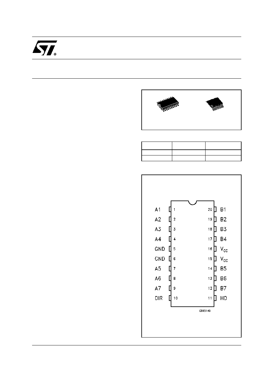
1 - 4
A1 - A4
Side A Input or Output
5, 6
GND
Ground
7 - 9
A5 - A7
Side A Input
10
DIR
Direction Control Input
11
HD
High Drive Enable Input
12 - 14
B5 - B7
Side B Output
15, 16
V
CC
Power Supply
INPUT
FUNCTION
OUTPUTS
DIR
HD
L
L
B1 - B4 Data to A1 - A4
A5 - A7 Data to B5 - B7
B5 - B7 Open Drain
L
H
B5 - B7 Totem Pole
H
L
A1 - A7 Data to B1 - B7
B1 - B7 Open Drain
H
H
B1 - B7 Totem Pole

74ACT1284
3/11
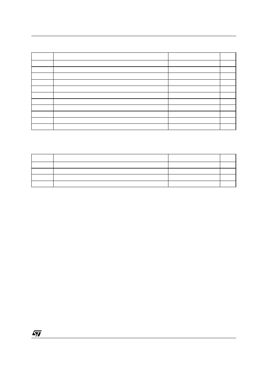
ABSOLUTE MAXIMUM RATINGS
Absolute Maximum Ratings are those values beyond which damage to the device may occur. Functional operation under these conditions is
not implied.
(1) The AC input voltage pulse width is limited to 20ns if the input voltage goes more negative than -0.5V.
RECOMMENDED OPERATING CONDITIONS
Symbol
Parameter
Value
Unit
V
CC
Supply Voltage
-0.5 to +7
V
V
IA
DC Input Voltage A Side
-0.5 to V
CC
+ 0.5
V
V
IB
DC Input Voltage B Side
-2 to +7
(1)
V
V
OA
DC Output Voltage A Side
-0.5 to V
CC
+ 0.5
V
V
OB
DC Output Voltage B Side
-2 to +7
(1)
V
I
IK
DC Input Diode Current
±
20
mA
I
OK
DC Output Diode Current
±
50
mA
I
O
DC Output Current
±
50
mA
I
CC
or I
GND
DC V
CC
or Ground Current
±
200
mA
T
STG
Storage Temperature
-65 to +150
∞C
T
L
Lead Temperature (10 sec)
300
∞C
Symbol
Parameter
Value
Unit
V
CC
Supply Voltage
4.5 to 5.5
V
V
I
Input Voltage
0 to V
CC
V
V
O
Output Voltage
HD = LOW
0 to 5.5
V
T
op
Operating Temperature
-40 to 85
∞C

74ACT1284
4/11
DC ELECTRICAL CHARACTERISTICS
AC ELECTRICAL CHARACTERISTICS (f = 1MHz, t
r
= t
f
= 2.5ns)
Symbol
Parameter
Test Condition
Value
Unit
V
CC
(V)
T
A
= 25∞C
-40 to 85∞C
Min.
Typ.
Max.
Min.
Max.
V
IH
High Level Input Voltage
4.5 to 5.5
2.0
2.0
V
V
IL
Low Level Input Voltage
4.5 to 5.5
0.8
0.8
V
V
OHB
High Level Output Voltage
B Port
4.5
I
OH
= -14mA
3.86
3.76
V
V
OHA
High Level Output Voltage
A Port
4.5
I
O
= -50
µ
A
4.4
4.4
V
I
O
= -4mA
3.86
3.76
V
OLB
Low Level Output Voltage
B Port
4.5
I
OH
= 14mA
0.4
0.4
V
V
OLA
Low Level Output Voltage
A Port
4.5
I
O
= 50
µ
A
0.1
0.1
V
I
O
= 4mA
0.36
0.44
I
I
Input Current
5.5
V
I
= V
CC
or GND
(DIR,A5,A6,A7,HD)
±
0.1
±
1
µ
A
I
CCT
Max I
CC
/Input
5.5
V
I
= V
CC
- 2.1V
0.6
1.5
mA
I
CC
Quiescent Supply Current
5.5
V
I
= V
CC
or GND
8
80
µ
A
I
OZ
Output Leakage Current
5.5
V
O
= V
CC
or GND
±
0.5
±
5
µ
A
I
OFF
B Side Power Down Leakage
Current
0
V
O
= 5.25V
4
40
µ
A
V
HYS
Input HysteresIs
5.0
V
T
+
= V
T
0.4
0.35
V
Z
O
Output Impedance B Port
5.0
V
B
= V
OH
8
24
Symbol
Parameter
Test Condition
Value
Unit
V
CC
(V)
T
A
= 25∞C
-40 to 85∞C
Min.
Typ.
Max.
Min.
Max.
t
PLH
Propagation Delay Time
A1 - A7 to B1 - B7
4.5 to 5.5
R
L
=500
, C
L
=50pF
(fig. 1-2)
1
5.6
1
6.5
ns
t
PHL
1
5.6
1
6.5
t
PLH
Propagation Delay Time
B1 - B4 to A1 - A4
4.5 to 5.5
R
L
=500
, C
L
=50pF
(fig. 3)
1
7.5
1
8.5
ns
t
PHL
1
7.5
1
8.5
t
EN
Enable Delay Time
HD to B1 - B7
4.5 to 5.5
R
S
=33
, R
L
=62
C
L
=50pF (fig. 2)
1
7.5
1
8.5
ns
t
DIS
Disable Delay Time
HD to B1 - B7
1
7.5
1
8.5
ns
t
r,
t
f
t
rise
, t
fall
B1 - B7 Open Drain
4.5 to 5.5
R
PULL_UP
=500
C
L
=50pF (fig. 4)
120
120
ns
C
I
Control Input Capacitance
(HD, DIR, A5 - A7)
Open
4
pF
C
I/O
I/O Pin Capacitance
5.0
12
pF

74ACT1284
5/11
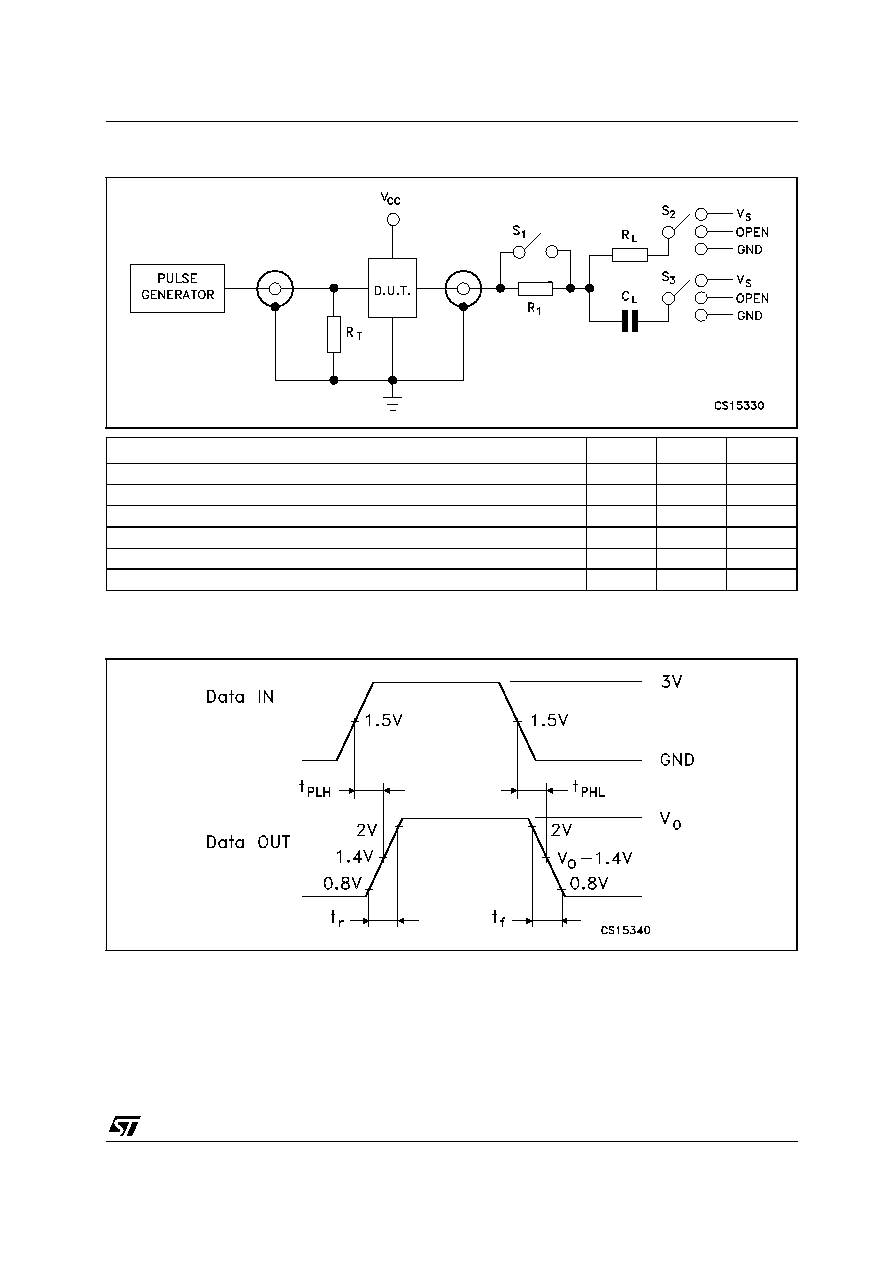
TEST CIRCUIT
C
L
= 50 pF or equivalent (includes jig and probe capacitance)
R
T
= Z
OUT
of pulse generator (typically 50
)
Figure 1 : Propagation Delay Time
TEST
S1
S2
S2
t
PHL
(A1-A7 to B1-B7) R
L
= 62
,
R
1
= 33
(
see waveform 1)
OPEN
V
CC
V
CC
t
PLH
(A1-A7 to B1-B7) R
L
= 62
(see waveform 1)
CLOSED
GND
GND
t
PHL
, t
PLH
(B1-B4 to A1-A4) R
L
= 500
(see waveform 2)
CLOSED
GND
GND
t
r
, t
f
(A1-A7 to B1-B7) R
L
= 500
(see waveform 1)
CLOSED
V
CC
V
CC
t
EN
(HD to B1-B7) R
L
= 62
,
R
1
= 33
(see waveform 3)
OPEN
GND
GND
t
DIS
(HD to B1-B7) R
L
= 62
(see waveform 3)
CLOSED
GND
GND
