
SNAD02C
8-CHANNEL 10-BIT ADC
======== CONTENTS ========
1.
GENERAL DESCRIPTION.......................................................................................................................................3
2.
FEATURES....................................................................................................................................................................3
3.
APPLICATIONS ..........................................................................................................................................................3
4.
BLOCK DIAGRAM.....................................................................................................................................................4
5.
PIN ASSIGNMENTS ...................................................................................................................................................4
6.
FUNCTIONAL DESCRIPTIONS .............................................................................................................................5
6.1.
I
NTERFACE
F
ORMAT
..................................................................................................................................5
6.2.
C
HANNEL
S
ETTING
....................................................................................................................................7
6.3.
C
ONTROL
R
EGISTER
S
ETTING
...................................................................................................................7
6.4.
ADC R
EAD
T
IMING
..................................................................................................................................8
6.5.
T
IMING OF
D
IGITAL
I
NPUT
R
EADING
........................................................................................................9
6.6.
P
OWER
D
OWN
& C
HANNEL
W
AKE
-U
P
..................................................................................................10
6.7.
B
ANDGAP REFERENCE
.............................................................................................................................11
6.8.
I
NPUT
C
HANNEL
PAD (C
HANNEL
0~6) .................................................................................................12
6.9.
B
ATTERY
M
ONITORING
(C
HANNEL
7
ONLY
) .........................................................................................13
7.
ELECTRICAL CHARACTERISTICS ..................................................................................................................14
8.
APPLICATION CIRCUITS.....................................................................................................................................15
9.
EXAMPLE PROGRAMS .........................................................................................................................................16
9.1.
P
ROGRAM
1: S
ET
C
ONFIGURATION OF
SNAD02C...............................................................................23
9.2.
P
ROGRAM
2: R
EAD
ADC
RESULT FROM
C
HANNEL
1...........................................................................23
9.3.
P
ROGRAM
3: R
EAD
D
IGITAL
I
NPUT DATA FROM
C
H
4, C
H
3, CH2 .......................................................23
9.4.
P
ROGRAM
4: P
OWER
-
DOWN
SNAD02C
AND
H
OST
,
AND
W
AKE
-
UP
...................................................24
9.5.
P
ROGRAM
5: B
ATTERY
L
OW
D
ETECTION
..............................................................................................24
10.
PAD DIAGRAM...................................................................................................................................26
Version: 1.3
July 31, 2003
1

SNAD02C
8-CHANNEL 10-BIT ADC
AMENDMENT HISTORY
Version Date
Description
Ver 1.1
February 12, 2003 First issue.
Ver 1.2
March 18, 2003
Page3: wording modification in FEATURES list
Page8: modify Table-3 control register setting
Page10: modify Figure-10
Page11: "enters into power down mode at the
8
th
clock cycle"
Page11: more descript about power-down mode setting
Ver 1.3
July 31, 2003
1. Add version code "C" of chip no.
2. Page23:
MB=1
3. This spec is modified form SNAD02_V1.2
Note:
This document is used to identify the different version "B" & "C" of SNAD01, the
most important is standby current and power down setting between version "B" &
"C". For the detail please refer to related section.
Version: 1.3
July 31, 2003
2

SNAD02C
8-CHANNEL 10-BIT ADC
1. GENERAL DESCRIPTION
SNAD02C is a low cost serial 10-bits ADC with 8 individual input channels. Each channel can be
independently programmed to a digital or analog input mode. In the analog input mode, this
single-ended channel accepts an analog input signal from 0 to V
REF
and converts the signal into
12-bit digital codes (with 10-bit accuracy guaranteed). In the digital input mode, the channel can be
treated as digital input port and the logic level appears at the channel can be acquired. SNAD02C
has a synchronous 3-wires serial interface. Through this interface, the host CPU can easily control
SNAD02C.
During A-to-D conversion, the typical current consumption is 500uA at 25kHz throughput-rate and
+3V power supply. SNAD02C includes a power-down mode, which reduces maximum current
consumption less than 1uA.
The reference voltage can be varied between 1V and +V
CC
, providing a corresponding input
voltage range of 0V to V
REF
. SNAD02C also has an on-chip 1.17V bandgap reference that can be
utilized for constant voltage input (especially for battery monitoring applications). The bandgap
reference circuitry consumes 300
�A@3v and can be enabled and disabled.
2. FEATURES
Single Supply: 2.7V ~ 5.25V
Eight Analog/Digital Input Channels.
Internal 1.17v Bandgap Reference for Battery Monitoring. (Channel 7)
Low Power Consumption: typical operating current: 500uA @ 3V, Standby current <1uA.
Up to 25kHz Conversion Rate.
12-bits ADC with 8-bit effective number of bits
3-Wire Serial Interface.
3. APPLICATIONS
Battery-Powered Systems
Instrumentation
Portable Data Logging
Test Equipment
Data Acquisition
Process-Control Monitoring
Digital Input Bus Extender
Version: 1.3
July 31, 2003
3
SNAD02C
8-CHANNEL 10-BIT ADC
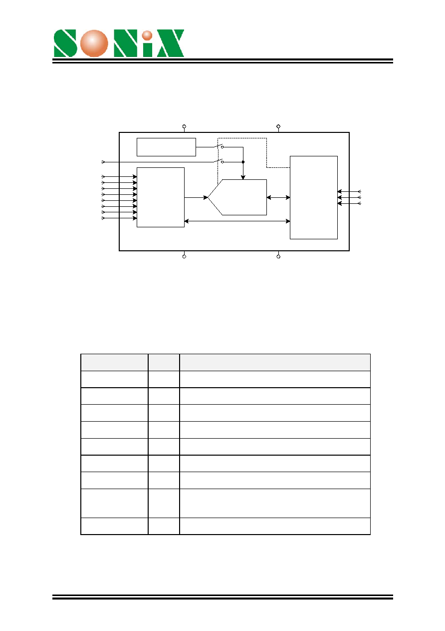
4. BLOCK DIAGRAM
8-Channels
Analog/Digital
Input MUX
12 Bit SAR
ADC
Serial
Interface
and
Control
Logic
VRH
START
CLK
DIO
AVDD
VDD
D
AVSS
VSSD
CH0/DI0
CH1/DI1
CH2/DI2
CH3/DI3
CH4/DI4
CH5/DI5
CH6/DI6
CH7(BAT)/DI7
1.2V Bandgap
Reference
Figure-1 Block diagram of ADC
5. PIN ASSIGNMENTS
Pin Name
I/O
Description
CH[7] ~ CH[0]
I
Analog input / digital input
REF
I
Reference voltage of analog signal
VDD
I
Positive power
VSS I
Negative
power
AVDD
I
Positive power of analog circuit
AVSS
I
Negative power of analog circuit
START
I
Command initialization signal (from host controller)
CLK
I
Clock of data communication and AD conversion (from
host controller)
DIO
IO
Data input and output of data communication
Table-1
Version: 1.3
July 31, 2003
4
SNAD02C
8-CHANNEL 10-BIT ADC
6. Functional Descriptions
Host CPU
Output Port1
Output Port2
I/O port
SNAD02
START
CLK
DIO
START
CLK
DIO
VDD
AVDD
REF
VDD
`
VSS
AVSS
CH[0]
CH[1]
CH[7]
Analog/Digital
Signal
0.1uF
Figure-2 Interface with Host CPU
6.1. Interface
Format
Channel Setting
Control Register Setting
HiZ
CM2
CM1
CM0
PH
PL
RF
MB
X
X
X
X
X
X
X
X
X
DIO
Digital Input Reading
Power Down
CLK
START
HiZ
CM2
CM1
CM0
CH[7] CH[6] CH[5]
CH[4] CH[3]
CH[2] CH[1]
CH[0]
X
X
X
X
X
DIO
HiZ
CM2
CM1
CM0
DI[7]
DI[6]
DI[5]
DI[4]
DI[3]
DI[2]
DI[1]
DI[0]
DI[3]
DI[7]
DI[6]
DI[5]
DI[4]
DIO
Port Input
Port Output
Port Input
HiZ
CM2
CM1
CM0
PDS
PDS
PDS
PDS
PDS
PDS
PDS
PDS
PDS
PDS
PDS
PDS
PDS
DIO
Port Output
Port Input
Port Input
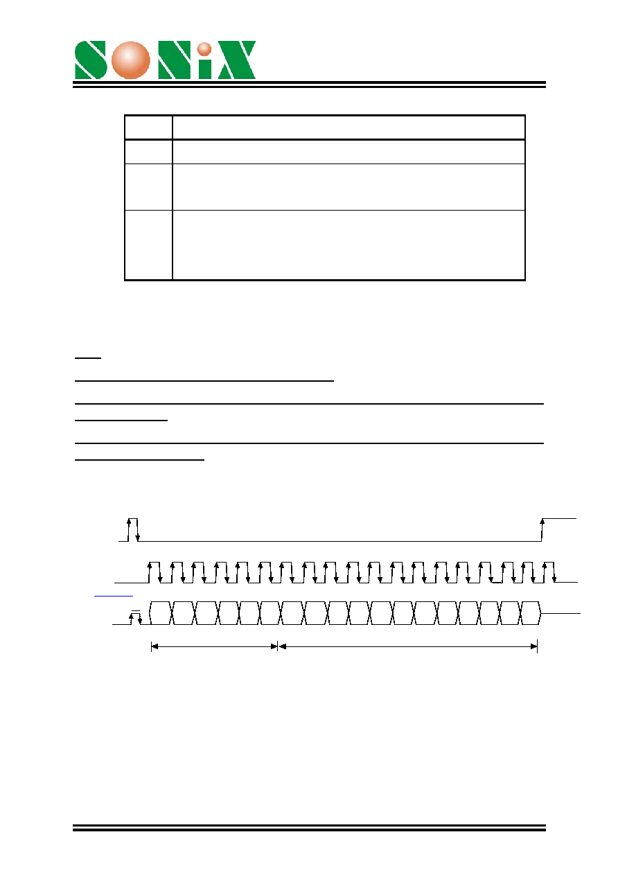
Figure-3 Timing Diagram of Whole Commands
Version: 1.3
July 31, 2003
5
SNAD02C
8-CHANNEL 10-BIT ADC
(1) DIO is HiZ while START is HIGH.
(2) The interface logic begins to interpret a command at the falling edge of the START signal.
(3) The command ID (sent by Host) is received in the first three clock cycles from DIO.
(4) The operations include Channel setting, ADC Reading, Digital Input Reading and Power
Down.
(5) DIO becomes to HiZ while START returns to HIGH.
Command ID
Operation
000
Power Down (0)
001
Channel Attribute Setting (1:Analog, 0:Digital)
010
Channel Wakeup Function Setting
(1:Enable, 0:Disable)
011
Control Register Setting
100 ADC
Conversion
101
Digital Input Reading
110 Reserved
111
Power Down (1)
Table-2 Command Description Table
a. 000/111: ADC enters into power down after receiving this command.
b. 001: Set the attribute of each channel to be an analog or a digital input with the sequence of
channel 7 to 0. (1:Analog; 0:Digital)
c.
010: Set the wakeup function of each channel to be enabled or disabled with the sequence of
channel 7 to 0. (1:Enable; 0:Disable)
d. 011: Setting the values of control registers.
e. 100: ADC starts to convert the analog signal of the selected channel after receiving this
command.
f.
101: ADC starts to read the digital input of every channel with the sequence of channel 7 to 0.
g. 110: ADC enters into testing mode.
Version: 1.3
July 31, 2003
6
SNAD02C
8-CHANNEL 10-BIT ADC
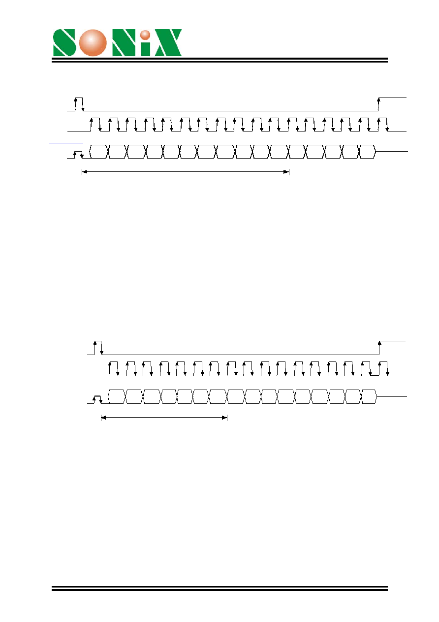
6.2. Channel
Setting
CLK
START
Channel Setting
HiZ
CM2
CM1
CM0
CH[7] CH[6] CH[5] CH[4]
CH[3] CH[2] CH[1]
CH[0]
X
X
X
X
X
DIO
Port Input
Figure-4 The timing diagram of channel attribute/wakeup setting
(1) Command 001: channel attribute setting.
(2) Command 010: wakeup function setting.
In attribute setting, "1" means analog and "0" means digital. In wakeup setting, "1" means enable
and "0" means disable. After all of the channels are set, the DIO port remains input mode and all
the following data are ignored.
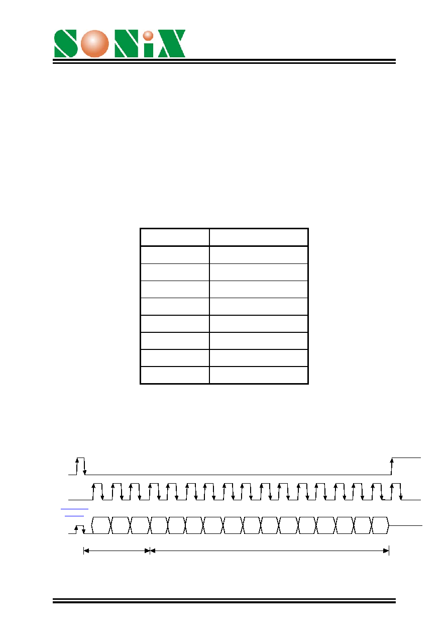
6.3. Control Register Setting
CLK
START
Control Register Setting
HiZ
CM2
CM
1
CM0
PH
PL
RF
MB
X
X
X
X
X
X
X
X
X
DIO
Port Input
Figure-5 The timing diagram of control registers setting
(1) Command ID: (011)
(2) 4-bit data behind command ID are loaded into control registers with the sequence of PH, PL,
RF and MB.
(3) The function of each control registers are as Table-3.
Version: 1.3
July 31, 2003
7
SNAD02C
8-CHANNEL 10-BIT ADC
Name Function
PH
Set the pull-up resistor of the channel in digital input mode. 1:ON, 0:OFF.
PL
Set the pull-down resistor of the channel in digital input mode.
"1": ON, "0": OFF.
RF, MB Set the reference source (from internal bandgap or "REF" pin)
RF=0, MB=1: reference voltage from "REF" pin
RF=1, MB=0: reference voltage from internal bandgap
Table-3
Note:
1. The condition of both PH=1 and PL=1 is prohibited.
2. Pull-up and pull-down resistors are not activated while the corresponding channel is set as
analog input mode.
3. Before into power down mode, the "RF" and "MB" register must set up "0", otherwise the standby
current will more than 1uA.
6.4. ADC Read Timing
START
ADC Reading
HiZ
CM2
CM1
CM0
ID2
ID1
ID0
X
X
D9
D8
D7
D2
D6
D5
D4
D3
DIO
D0
D1
Port Input
Port Output
CLK
Figure-6 The timing diagram of ADC reading
Version: 1.3
July 31, 2003
8
SNAD02C
8-CHANNEL 10-BIT ADC
(1) Command ID: (100)
(2) 3-bit channel number data behind command ID.
(3) The analog signal of the selected channel is sampled to ADC. ADC refers the reference
voltage and converts the sampled analog signal to digital domain by successive-
approximation method.
(4) The 10-bit output data (result of conversion) of ADC is sent to DIO port from MSB and is
triggered by CLK. The maximum clock frequency is 500kHz @ 2.7v. (Maximum conversion
rate=25KHz)
(5) After the 10-bits ADC data has been sent out, if the START is kept in LOW and CLK is kept in
High/Low transition, then the data with uncertain value are kept appearing on DIO. These
data can just be ignored.
Channel ID[2:0]
Selected Channel
000 CH0
001 CH1
010 CH2
011 CH3
100 CH4
101 CH5
110 CH6
111 CH7
Table-4 Channel Selection Table
6.5. Timing of Digital Input Reading
CLK
START
Digital Input
Reading
HiZ
CM
2
CM
1
CM0
DI[7] DI[6] DI[5] DI[4]
DI[3] DI[2] DI[1] DI[0]
DI[3]
DI[7] DI[6] DI[5] DI[4]
DIO
Port Output
Port Input
Figure-7 The timing diagram of the digital input reading
Version: 1.3
July 31, 2003
9
SNAD02C
8-CHANNEL 10-BIT ADC
(1) Command ID: (101).
(2) The digital data of each channel is sent to the DIO port with the sequence of channel 7 to 0.
(3) After all of the channels are read, if the START is kept in LOW and CLK is kept in HIGH/LOW
transition, the digital data of each channel is sent to the DIO port again with the sequence of
channel 7 to 0 cyclically.
(4) Pulling START to HIGH to terminates this digital input reading.
Note: Once a channel is programmed as analog type, the corresponding data is "0" in digital input
reading command.
6.6. Power Down & Channel Wake-Up
0
0
0
1
1
1
SNAD01 enters into
power-down mode
START
CLK
DIO
DIO
Figure-8 The timing diagram of power down command
START
CLK
CH n
CH n
DIO
DIO
Wake-Up
Host CPU
HiZ
HiZ
Wake-Up
Procedure Ending
Figure-9 The timing diagram of power down command
Version: 1.3
July 31, 2003
10
SNAD02C
8-CHANNEL 10-BIT ADC
(1) The power down command (000/111) is sent to SNAD02C in the first three cycles, and then
SNAD02C enters into power down mode at the 8
th
clock cycle, consuming almost no current
(less than 1uA).
(2) After SNAD02C enters power down (mode 0: command 000), SNAD02C sends "0" out to
DIO until a valid logic transition appears on any wakeup-enabled digital input channel. Once
the transition occurs, SNAD02C toggles DIO to "1" to inform host controller. After receiving
"1" from DIO, host controller should turn START back to "1" to inform SNAD02C that the
power-down stage is over. Otherwise, SNAD02C keeps sending out "1" to DIO and does not
recognize any other transitions on any channels.
(3) After SNAD02C enters power down (mode 1: command 111), SNAD02C sends "1" out to
DIO until a valid logic transition appears on any wakeup-enabled digital input channel. Once
the transition occurs, SNAD02C toggles DIO to "0" to inform host controller. After receiving
"0" from DIO, host controller should turn START back to "1" to inform SNAD02C that the
power-down stage is over. Otherwise, SNAD02C keeps sending out "1" to DIO and does not
recognize any other transitions any the channels.
(4) The CLK may stop but START ought to remain at LOW level in the whole power down mode.
(5) The SNAD02C provides two power-down mode "POWER_DOWN 0" and
"POWER_DOWN 1", user has to select a property power-down mode that it depend
on what kind I/O type for host MCU (pull-up or pull-low) before ADC enter
power-down mode. Otherwise, it will generate a DC-path and the standby current
also will go up.
(6) Before into power down mode, the "RF" and "MB" register must set up "0", otherwise
the standby current will more than 1uA.
Note:
Wakeup function is only dedicated to the channel which is digital input type AND wakeup-enabled.
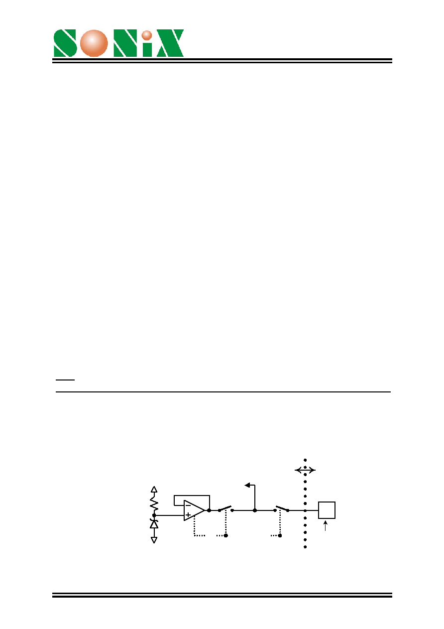
6.7. Bandgap
reference
VDD
VSS
REF
PAD
to reference
high of the ADC
RF
MB
1.2v
bandgap
reference
ON CHIP
OFF CHIP
Figure-10 Circuit diagram of ADC bandgap reference selection
Version: 1.3
July 31, 2003
11
SNAD02C
8-CHANNEL 10-BIT ADC
If the internal bandgap reference is turned ON (RF=1), the reference voltage "VREF" of ADC is
from the internal bandgap reference circuit. This internal voltage reference circuit consumes
around 300
�A, and the output voltage of bandgap reference is around 1.17V typically.
If RF is turned off (RF=0), the MB is turned on (MB=1), the reference voltage is from "REF" pin.
Otherwise, the reference voltage source is comes from internal bandgap if RF=1 & MB=0.
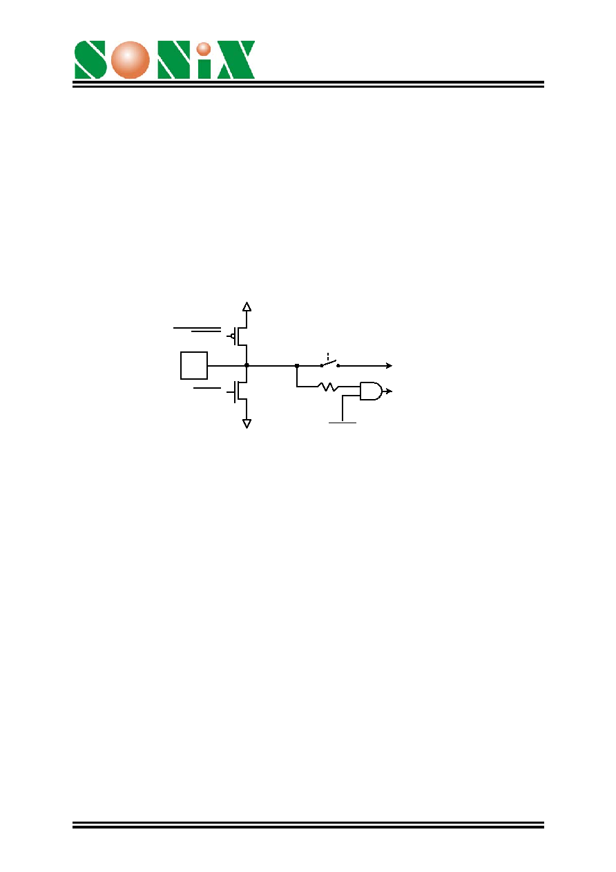
6.8. Input Channel PAD (Channel 0~6)
VDD
VSS
ENCH[x]
to ADC
DI[x]
CH[x]
ENCH[x]
Pull-high resistor
Pull-low resistor
ENCH[x]: 1: Analog In / 0: Digital In
PH&ENCH[x]
PL&ENCH[x]
Figure-11 Circuit diagram of the Input Channel PAD
(1) If any channel is programmed to be analog input mode, then the corresponding internal
signal, ENCH[x]=1. As in Figure-11, pull-high and pull-low are disabled. And the path to
digital input is blocked. All digital reading operation of this channel will get the result "0".
(2) If any channel is programmed to digital input mode, then the corresponding internal signal,
ENCH[x]=0. As in Figure-11, the path to ADC is removed.
(3) While in digital input mode, this input port can be configured to be floating, weak pull-up, or
pull-down by setting the control register PH and PL, where PH&PL=1 is forbidden. The
pull-up or pull-low resister are both around 500K
@3v.
(4) The default status (digital/analog, pull up/down) of all the channels are un-know after power
on, so initialize each channel to define a correct state should be done after power on.
(5) Mode of each channel (ENCH[x]) can be set by command 001.
Version: 1.3
July 31, 2003
12
SNAD02C
8-CHANNEL 10-BIT ADC
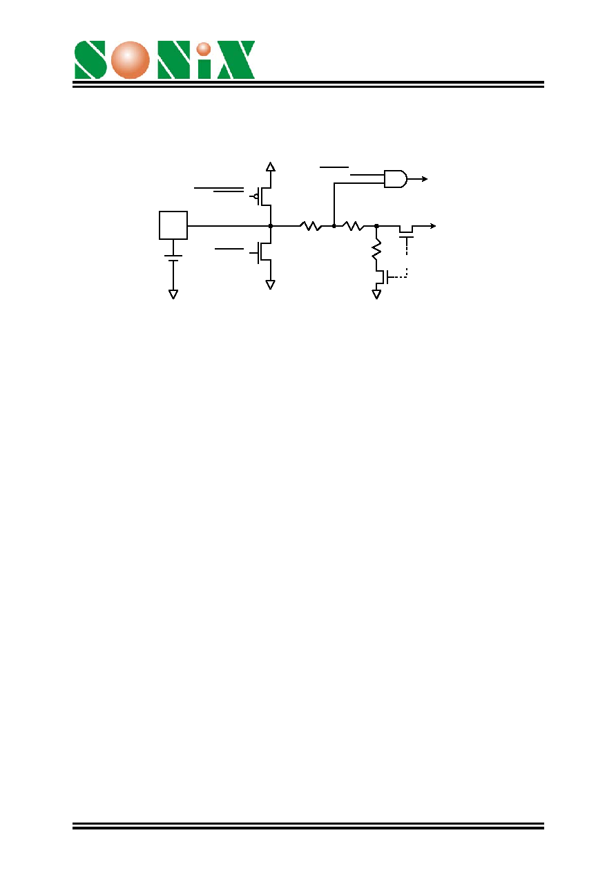
6.9. Battery Monitoring (Channel 7 only)
ENCH[7]
to ADC
DI[7]
VSS
20k
10k
30k
VSS
Battery
ENCH[7]
VDD
VSS
CH[7]
PH&ENCH[x]
PL&ENCH[x]
Figure-12 The circuit of the Input pad of Channel 7
(1) While read ADC command is sent and channel 7 is selected, ADC can be used to monitor the
battery voltage.
(2)
The circuit of battery voltage monitoring is shown in Figure-12 (Channel7 only)
(3) The battery voltage is six times ADC measuring voltage. Thus, the measured result equals to
1/6*battery voltage.
(4) While channel 7 is set to the analog input mode, an input resistor (60k
) exists from CH[7] to
VSS. To save unnecessary power consumption, CH[7] should be switch to digital input type
when CH[7] is not measured.
Note:
CH[7] is different from the other 7 channels. The input voltage is reduced to 1/6 before it is sent into
ADC.
Version: 1.3
July 31, 2003
13

SNAD02C
8-CHANNEL 10-BIT ADC
7. ELECTRICAL CHARACTERISTICS
Typical values apply for V
DD
=V
REF
=3.0 V, T
AMB
=25
�C unless otherwise noted.
Symbol Parameter min
typ
max
Unit Conditions
Analog-to-Digital Converter
V
DD
Operating
voltage 2.7
3.0
5.25
V
I
DD
Operating
current 400
650
�A
Excluding bandgap reference
and Control Register's RF is
set up 0 .
V
DD
=3.0V
I
PDN
Power Down Current
0.1
�A V
DD
=3.0V
F
SMP
Conversion
Rate
(Throughput Rate)
30
40
kHz
V
DD
=3.0V
V
DD
=5.0V
DNL Differential
Nonlinearity
�0.5
LSB
INL Integral
Nonlinearity
�-0.5
LSB
NMC
No Missing Code
10
Bits
V
DD
=2.7~5.25V
SINAD
Signal to Noise and
Distortion
50
dB
ENOB
Effective Number of Bits
10
Bits
Bandgap reference
VBG
Bandgap reference output
voltage
1.14 1.17 1.20
V
IBG
Operating current of BGR
400
�A
Digital Interface
Weak pull up/down
resistance
500k
V
DD
=3V
Output drive/sink current of
DIO
3
mA
V
OP
=V
DD
-0.5v/V
SS
+0.5v
Version: 1.3
July 31, 2003
14
SNAD02C
8-CHANNEL 10-BIT ADC
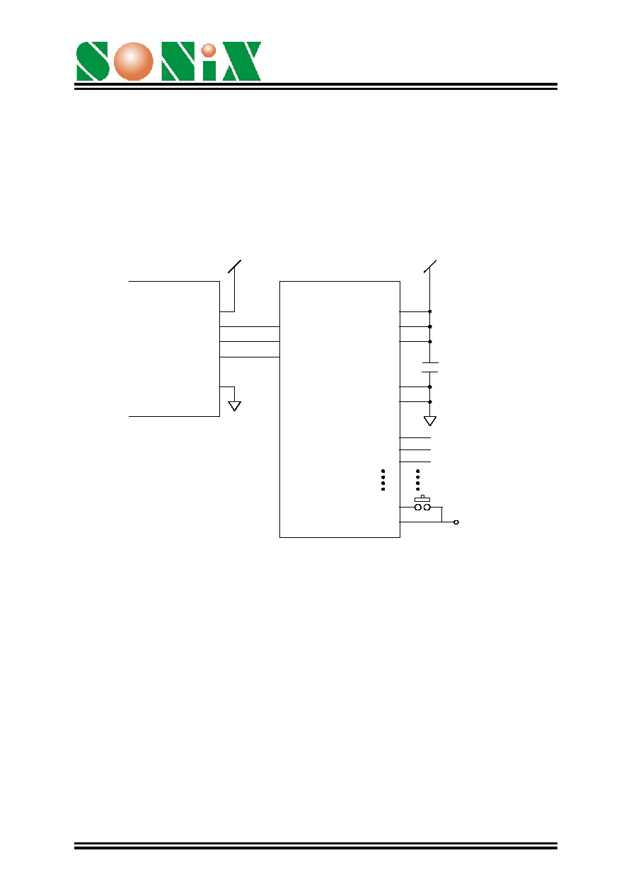
8. APPLICATION CIRCUITS
Example Circuit: SNAD02C works with Sonix 4-bit Series Controller
CH[0], CH[1], CH[2]: Analog Input
CH[6]: Digital Input
CH[7]: Battery Voltage Detect
REF=VDD+
4-bit Voice chip
P22
SNAD02
START
CLK
DIO
VDD
AVDD
REF
VDD
`
VSS
AVSS
CH[0]
CH[1]
CH[7]
Analog Signal
0.1uF
VDD
P21
P20
VSS
SN100/300/500
SN66/67/68/6A
Analog Signal
CH[2]
Analog Signal
CH[6]
VDD
Figure-13
SNAD02C works with Sonix 4-bit Series Controller
Version: 1.3
July 31, 2003
15

SNAD02C
8-CHANNEL 10-BIT ADC
9. EXAMPLE PROGRAMS
Host Controller: SNC500. Application circuit is identical to Figure11. P22: START. P21:
CLK. P20: DIO.
Macro Programs: (def.h)
p2State
equ
m0
port_l
equ
m1
port_h
equ
m2
ad_out_l equ
m3
ad_out_h equ
m4
tmp equ
m5
tmp1
equ
m6
ad_hh
equ
m7
;;********************************
@ON_START macro
;;SET START=0
mov a #1011b
and a p2state
mov p2state a
mov p2 a
endm
;;********************************
@OFF_START macro
;;SET START=1
mov a #0100b
or a p2state
mov p2state a
mov p2 a
endm
;;********************************
@CLOCK macro
mov a #0010b
;;SET CLK L H AND H L
or a p2state
mov p2 a
mov a #1101b
and a p2state
mov p2state a
mov p2 a
endm
;;********************************
@Send_0 macro
mov a #1110b
;;HOST SEND 0 DIO
and a p2state
mov p2state a
mov p2 a
endm
;;********************************
@Send_1 macro
mov a #0001b
;;HOST SEND 1 DIO
or a p2state
mov p2state a
mov p2 a
endm
;;********************************
@Send macro data
;
;HOST SEND 1-BIT CONSTANT (#1 OR #0) DIO
mov tmp data
mov a #1110b
and a p2state
or a tmp
mov p2state a
mov p2 a
endm
Version: 1.3
July 31, 2003
16
;;********************************

SNAD02C
8-CHANNEL 10-BIT ADC
@Read_DIO macro
;;READ DIO A.0 (1-BIT)
mov a p2
mov tmp #0001b
and a tmp
endm
;;********************************
@P20_Out_Mode macro
;
;SWITCH ALL 4-BIT OF P2 TO OUTPUT MODE
mov a #0000b
mov p2s a
endm
;;********************************
@P20_In_Mode macro
;
;SWITCH P2.0 (DIO) TO INPUT MODE
mov a #0001b
mov p2s a
mov a #1110b
and a p2state
mov p2state a
mov p2 a
endm
;;**************************************************************************
;; Set Analog/Digital Mode to each channel (1:Analog, 0:Digital) *
;; y7 Ch7. y6 Ch6. y5 Ch5, ...
*
;;**************************************************************************
@Set_Attrib macro y7,y6,y5,y4,y3,y2,y1,y0
@P20_Out_mode
;; SWITCH P2 TO OUTPUT MODE
@ON_START
;; SET START=0
@Send_0
;; SEND COMMAND (001)
@Clock
@Send_0
@Clock
@Send_1
@Clock
@Send y7
;; SEND y7 TO y0
@Clock
@Send y6
@Clock
@Send y5
@Clock
@Send y4
@Clock
@Send y3
@Clock
@Send y2
@Clock
@Send y1
@Clock
@Send y0
@Clock
@OFF_START
;; SET START=1
@P20_In_mode
;; SWITCH P2.0 TO INPUT MODE
endm
Version: 1.3
July 31, 2003
17

SNAD02C
8-CHANNEL 10-BIT ADC
;;*************************************************************************
;; Set Wakeup function Enable/Disable (1:Enable, 0:Disable) *
;; y7 Ch7. y6 Ch6. y5 Ch5, ...
*
;;*************************************************************************
@Set_Wakeup macro y7,y6,y5,y4,y3,y2,y1,y0
@P20_Out_mode
;; SWITCH P2 TO OUTPUT MODE
@ON_START
;; SET START=0
@Send_0
;; SEND COMMAND (010)
@Clock
@Send_1
@Clock
@Send_0
@Clock
@Send y7
;; SEND y7 TO y0
@Clock
@Send y6
@Clock
@Send y5
@Clock
@Send y4
@Clock
@Send y3
@Clock
@Send y2
@Clock
@Send y1
@Clock
@Send y0
@Clock
@OFF_START
;; SET START=1
@P20_In_mode
;; SWITCH P2.0 TO INPUT MODE
endm
;;**********************************************************************
;;
Setup
Control
Register
*
;; ph: PULL-HIGH register. pl:PULL-LOW register.
*
;;
rf:
BANDGAP
reference
enable
*
;;
mb:
Set
0
always
*
;;**********************************************************************
@Set_Control_Reg macro ph,pl,rf,mb
@P20_Out_mode
;; SWITCH P2 TO OUTPUT MODE
@ON_START
;; SET START=0
@Send_0
;; SEND COMMAND (011)
@Clock
@Send_1
@Clock
@Send_1
@Clock
@Send ph
;; SEND ph, pl, rf, mb
@Clock
@Send pl
@Clock
@Send rf
@Clock
@Send mb
@Clock
@OFF_START
;; SET START=1
@P20_In_mode
;; SWITCH P2.0 TO INPUT MODE
endm
Version: 1.3
July 31, 2003
18

SNAD02C
8-CHANNEL 10-BIT ADC
;;*******************************************************************
;; Let SNAD02C Enter Power-Down mode 0
*
;;*******************************************************************
@Power_Down_0 macro
@P20_Out_mode
;; SWITCH P2 TO OUTPUT MODE
@ON_START
;; SET START=0
@Send_0
;; SEND COMMAND (000)
@Clock
@Send_0
@Clock
@Send_0
@Clock
@P20_In_mode
;; SWITCH P2.0 TO INPUT MODE
@Clock
@Clock
@Clock
@Clock
@Clock
@Clock
@Clock
@Clock
;; SNAD02C ENTERS POWER-DOWN AT THE 8-th CLOCK EDGE.
Endm
;;*****************************************************************
;; Let SNAD02C Enter Power-Down mode 1
*
;;*****************************************************************
@Power_Down_1 macro
@P20_Out_mode
;; SWITCH P2 TO OUTPUT MODE
@ON_START
;; SET START=0
@Send_1
;; SEND COMMAND (111)
@Clock
@Send_1
@Clock
@Send_1
@Clock
@P20_In_mode
;; SWITCH P2.0 TO INPUT MODE
@Clock
@Clock
@Clock
@Clock
@Clock
@Clock
@Clock
@Clock
;; SNAD02C ENTERS POWER-DOWN AT THE 8-th CLOCK EDGE.
endm
;;**************************************************************************
;; Read ADC from Channel n (n=n2,n1,n0)
;; e.g.: Ch 5 (n2, n1, n0= #1, #0, #1
;; 10-bit Data (ad_hh,ad_out_h, ad_out_l)
;; ad_hh is bit9~bit8 , ad_out_h is bit7~bit4 , ad_out_l is bit3~bit0
;;**************************************************************************
@Read_ADC macro n0, n1, n2
@P20_Out_mode
;; SWITCH P2 TO OUTPUT MODE
@ON_START
;; SET START=0
@Send_1
;; SEND COMMAND (100)
@Clock
@Send_0
@Clock
@Send_0
@Clock
@Send n2
;; SEND CHANNEL NUMBER
@Clock
@Send n1
@Clock
Version: 1.3
July 31, 2003
19

SNAD02C
8-CHANNEL 10-BIT ADC
@Send n0
@Clock
@p20_in_mode
;; SWITCH P2.0 TO INPUT MODE
@Clock
;; WAIT FOR 2 MORE CLOCKS
@Clock
mov ad_out_l #0
mov ad_out_h #0
mov ad_hh #0
;;***************************************
@Clock
;; READ DIO and SAVE 1-bit DATA in ad_hh.1
mov tmp1 #0010b
@Read_DIO
caje #0 @f
mov a ad_hh
or a tmp1
mov ad_hh
a
@@:
;;***************************************
@Clock
;; READ DIO and SAVE 1-bit DATA in ad_hh.0
mov tmp1 #0001b
@Read_DIO
caje #0 @f
mov a ad_hh
or a tmp1
mov ad_hh
a
@@:
;;***************************************
@Clock
;; READ DIO and SAVE 1-bit DATA in ad_out_h.3
mov tmp1 #1000b
@Read_DIO
caje #0 @f
mov a ad_out_h
or a tmp1
mov ad_out_h a
@@:
;;***************************************
@Clock
;; READ DIO and SAVE 1-bit DATA in ad_out_h.2
mov tmp1 #0100b
@Read_DIO
caje #0 @f
mov a ad_out_h
or a tmp1
mov ad_out_h a
@@:
;;***************************************
@Clock
;; READ DIO and SAVE 1-bit DATA in ad_out_h.1
mov tmp1 #0010b
@Read_DIO
caje #0 @f
mov a ad_out_h
or a tmp1
mov ad_out_h a
@@:
;;***************************************
@Clock
;
; READ DIO and SAVE 1-bit DATA in ad_out_h.0
mov tmp1 #0001b
@Read_DIO
caje #0 @f
mov a ad_out_h
or a tmp1
mov ad_out_h a
Version: 1.3
July 31, 2003
20

SNAD02C
8-CHANNEL 10-BIT ADC
@@:
;;***************************************
@Clock
;; READ DIO and SAVE 1-bit DATA in ad_out_l.3
mov tmp1 #1000b
@Read_DIO
caje #0 @f
mov a ad_out_l
or a tmp1
mov ad_out_l a
@@:
;;***************************************
@Clock
;; READ DIO and SAVE 1-bit DATA in ad_out_l.2
mov tmp1 #0100b
@Read_DIO
caje #0 @f
mov a ad_out_l
or a tmp1
mov ad_out_l a
@@:
;;***************************************
@Clock
;; READ DIO and SAVE 1-bit DATA in ad_out_l.1
mov tmp1 #0010b
@Read_DIO
caje #0 @f
mov a ad_out_l
or a tmp1
mov ad_out_l a
@@:
;;***************************************
@Clock
;
; READ DIO and SAVE 1-bit DATA in ad_out_l.0
mov tmp1 #0001b
@Read_DIO
caje #0 @f
mov a ad_out_l
or a tmp1
mov ad_out_l a
@@:
;;***************************************
@Clock
@OFF_START
;; SET START=1
endm
;;*****************************************************************
;; Read Digital Input:
*
;; 8-bit Data
(port_h,
port_l)
*
;;*****************************************************************
@Read_Port macro
@P20_Out_mode
;; SWITCH P2 TO OUTPUT MODE
@ON_START
;; SET START=0
@Send_1
;; SET COMMAND (101)
@Clock
@Send_0
@Clock
@Send_1
@Clock
@P20_In_mode
;; SWITCH P2.0 TO INPUT MODE
mov port_l #0
mov port_h #0
;;***************************************
@Clock
;; READ DIO and SAVE 1-bit DATA in port_h.3
mov tmp1 #1000b
@Read_DIO
Version: 1.3
July 31, 2003
21

SNAD02C
8-CHANNEL 10-BIT ADC
caje #0
@f
mov a port_h
or a
tmp1
mov port_h a
@@:
;;***************************************
@Clock
;; READ DIO and SAVE 1-bit DATA in port_h.2
mov tmp1 #0100b
@Read_DIO
caje #0
@f
mov a port_h
or a
tmp1
mov port_h a
@@:
;;***************************************
@Clock
;; READ DIO and SAVE 1-bit DATA in port_h.1
mov tmp1 #0010b
@Read_DIO
caje #0 @f
mov a port_h
or a tmp1
mov port_h a
@@:
;;***************************************
@Clock
;; READ DIO and SAVE 1-bit DATA in port_h.0
mov tmp1 #0001b
@Read_DIO
caje #0 @f
mov a port_h
or a tmp1
mov port_h a
@@:
;;***************************************
@Clock
;; READ DIO and SAVE 1-bit DATA in port_l.3
mov tmp1 #1000b
@Read_DIO
caje #0 @f
mov a port_l
or a tmp1
mov port_l a
@@:
;;***************************************
@Clock
;; READ DIO and SAVE 1-bit DATA in port_l.2
mov tmp1 #0100b
@Read_DIO
caje #0 @f
mov a port_l
or a tmp1
mov port_l a
@@:
;;***************************************
@Clock
;; READ DIO and SAVE 1-bit DATA in port_l.1
mov tmp1 #0010b
@Read_DIO
caje #0 @f
mov a port_l
or a tmp1
mov port_l a
@@:
;;***************************************
@Clock
;; READ DIO and SAVE 1-bit DATA in port_l.0
mov tmp1 #0001b
@Read_DIO
caje #0
@f
mov a port_l
or a
tmp1
mov port_l
a
Version: 1.3
July 31, 2003
22

SNAD02C
8-CHANNEL 10-BIT ADC
@@:
;;***************************************
@Clock
@OFF_START
;; SET START=1
endm
;;***************************************
9.1. Program 1: Set Configuration of SNAD02C
;; Setup Configuration of SNAD02C
;;
;; With Pull-Low, use "REF" pin connected external voltage . (PH=0, PL=1, RF=0,MB=1)
;;
;;
CH7 CH6 CH5 CH4 CH3 CH2 CH1 CH0
;; Analog/Digital: B A A D D D A A
:B, battery detect
;; Wakeup:
X X X NO YES YES X X
;;
SNC520
program
include def.h
START:
mov
a #1111b
mov
p2s
a
mov
a #0000b
mov
p2
a
mov
p2State
#0
@Set_Control_Reg
#0, #1, #0, #1
;; Set Control Registers
@Set_Attrib
#0, #1, #1, #0, #0, #0, #1, #1
;; Set Chan Analog/Digital
@Set_Wakeup
#0, #0, #0, #0, #1, #1, #0, #0
;; Setup Wakeup function
9.2. Program 2: Read ADC result from Channel 1
;; Inherit from program 1
;; 10-bit ADC result of channel 1 in ( ad_hh,ad_out_h, ad_out_l)
;; ad_hh is bit9~bit8, ad_out_h is bit7~bit4, ad_out_l is bit3~bit0
@Read_ADC
#0, #0, #1
;;get ADC result from Ch1 in ( ad_hh,ad_out_h, ad_out_l)
...
...
9.3. Program 3: Read Digital Input data from Ch4, Ch3, CH2
;; Inherit from program 1
;; After Reading,
;; Port_h.0 = Input of Ch4
;; Port_l.3 = Input of Ch3
;; Port_l.2 = Input of Ch2
@Read_Port
;; 8-bit Data (port_h, port_l)
...
...
Version: 1.3
July 31, 2003
23
SNAD02C
8-CHANNEL 10-BIT ADC
9.4. Program 4: Power-down SNAD02C and Host, and Wake-up
;; Inherit from program 1
;; Enter Power-down Mode (0)
@Set_Control_Reg #0, #1, #0, #0
;; Set Control Registers RF and MB is 0
@Power_Down_0
;;SNAD02 enters power-down Mode (0)
end
;; HOST(SNC520) enter power down
...
...
TRIGGER:
@OFF_START
;; SET START=1
...
@Read_Port
;; READ Trigger condition or Debounce Procedure starting from here
...
...
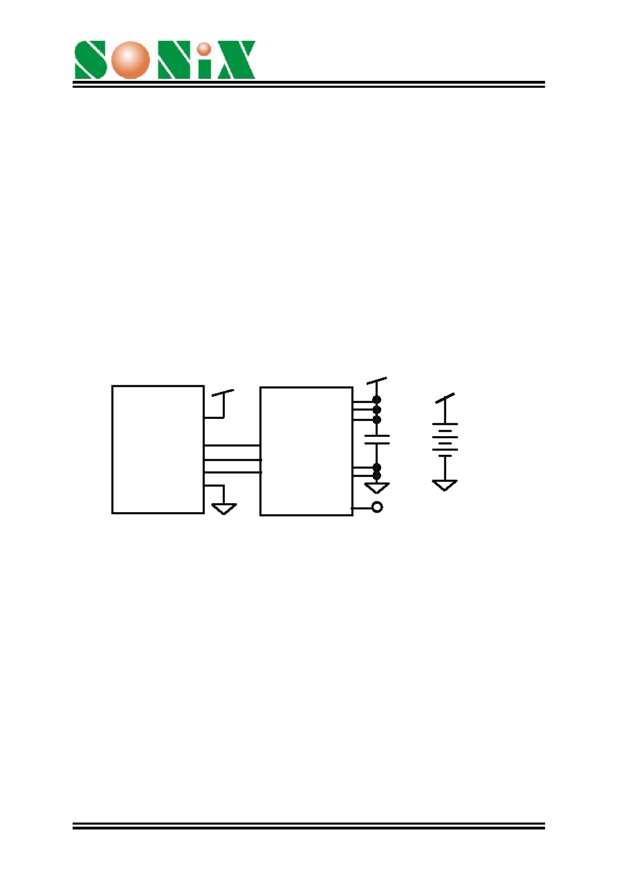
9.5. Program 5: Battery Low Detection
SNC520
SNAD02C
START
CLK
DIO
VDD
AVDD
REF
VSS
AVSS
CH[7]
VDD
0.1uF
VDD
VDD
VDD
VSS
P20
P21
P22
VDD
Battery:
1.5Vx3
An application uses three 1.5V batteries for power supply. During operation, the
power of batteries keeps consumed and the voltage of battery keeps going down.
Now, voltage lower than 3.6V is treated as "Battery Low". The ADC and band-gap
reference circuit in SNAD02 can be utilized to detect "Battery Low".
The voltage through channel 7 to ADC is reduced to 1/6*VDD (Figure10). Thus, when
VDD=3.6V, the voltage into ADC is around 0.6V. And bandgap is chosen for
reference voltage (approximately 1.17V within the whole operation voltage range).
The value acquired from ADC is about (0.6/1.17)*256=131. For simplification
consideration, we choose "ADC's readout < 128" as "Battery Low" condition.
Version: 1.3
July 31, 2003
24

SNAD02C
8-CHANNEL 10-BIT ADC
;; Inherit from program 1
;; Enter Power-down Mode (0)
CheckBattery:
@Set_Control_Reg #0,
#1,
#1,
#0
;; Set rf=1, turn-on bandgap
@Set_Attrib
#1,
#1, #1, #0, #0, #0, #1, #1
;; Switch Ch7 to Analog
mov
m15
#0
CheckAgain:
@Read_ADC
#1,
#1,
#1
;; Read Ch7
mov
a #1000b
and
a ad_out_h
caje
#1000b
Battery_Low_No
;; if (Value>=128) then Not Battery Low
mov
a m15
inca
mov
m15
a
caje
#3
Battery_Low_Yes
;; if (Value<128) for 3 times, then
jmp
CheckAgain
;; battery low.
Battery_Low_Yes:
mov
m14
#1
Battery_Low_No:
@Set_Control_Reg
#0, #1, #0, #0
;; Set rf=0, turn-off bandgap
@Set_Attrib
#0,
#1, #1, #0, #0, #0, #1, #1
;; Switch Ch7 to Digital
;; To save operating current
Version: 1.3
July 31, 2003
25
SNAD02C
8-CHANNEL 10-BIT ADC
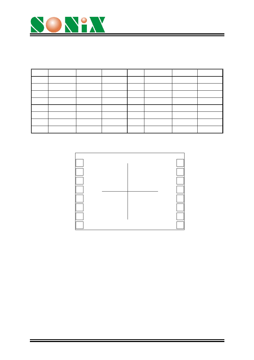
10. PAD DIAGRAM
NO
PAD NAME
X(um)
Y(um)
NO
PAD NAME
X(um)
Y(um)
1 CH0 -623.50
352.50
9 VSS 623.50
-417.50
2 CH1 -623.50
242.50
10 VDD 623.50
-307.50
3 CH2 -623.50
132.50
11 DIO 623.50
-197.50
4 CH3 -623.50
22.50
12 CLK 623.50
-87.50
5 CH4 -623.50
-87.50
13
START
623.50
22.50
6 CH5 -623.50
-197.50
14
AVDD
623.50
132.50
7 CH6 -623.50
-307.50
15 VSS 623.50
242.50
8 CH7 -623.50
-417.50
16 REF 623.50
352.50
CH0
CH1
CH2
CH3
CH4
CH5
CH6
CH7
1
2
10 VDD
11 DIO
12 CLK
START
13
14 AVDD
15 AVSS
16 REF
9
VSS
3
4
5
6
7
8
(0,0)
CHIP SIZE=1350 x 950um
SNAD02
Note: The substrate MUST be connected to Vss in PCB layout
Version: 1.3
July 31, 2003
26

SNAD02C
8-CHANNEL 10-BIT ADC
Version: 1.3
July 31, 2003
27
DISCLAIMER
The information appearing in SONiX web pages ("this publication") is believed to be
accurate.
However, this publication could contain technical inaccuracies or typographical errors.
The reader should not assume that this publication is error-free or that it will be suitable for
any particular purpose. SONiX makes no warranty, express, statutory implied or by
description in this publication or other documents which are referenced by or linked to this
publication. In no event shall SONiX be liable for any special, incidental, indirect or
consequential damages of any kind, or any damages whatsoever, including, without
limitation, those resulting from loss of use, data or profits, whether or not advised of the
possibility of damage, and on any theory of liability, arising out of or in connection with the
use or performance of this publication or other documents which are referenced by or
linked to this publication.
This publication was developed for products offered in Taiwan. SONiX may not offer the
products discussed in this document in other countries. Information is subject to change
without notice. Please contact SONiX or its local representative for information on
offerings available. Integrated circuits sold by SONiX are covered by the warranty and
patent indemnification provisions stipulated in the terms of sale only.
The application circuits illustrated in this document are for reference purposes only.
SONIX DISCLAIMS ALL WARRANTIES, INCLUDING THE WARRANTY OF
MERCHANTABILITY OR FITNESS FOR ANY PURPOSE. SONIX reserves the right to
halt production or alter the specifications and prices, and discontinue marketing the
Products listed at any time without notice. Accordingly, the reader is cautioned to verify
that the data sheets and other information in this publication are current before placing
orders.
Products described herein are intended for use in normal commercial applications.
Applications involving unusual environmental or reliability requirements, e.g. military
equipment or medical life support equipment, are specifically not recommended without
additional processing by SONIX for such application.