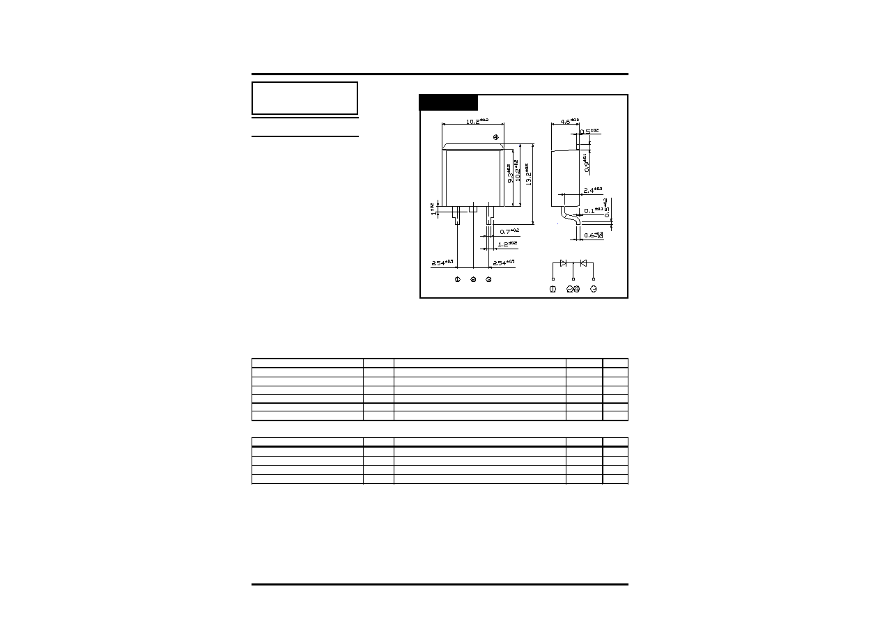
DF30JC4
40V 30A
Copyright & Copy;2001 Shindengen Electric Mfg.Co.Ltd
OUTLINE DIMENSIONS
RATINGS
SHINDENGEN
Case : STO-220
Unit : mm
Dual
Shottky Rectifiers (SBD)
Absolute Maximum Ratings iUnless otherwise specified, Tc=25j
Item
Symbol
Conditions
Ratings
Unit
Storage Temperature
Tstg
-55`150
Operating Junction Temperature
Tj
150
Maximum Reverse Voltage
V
RM
40
V
Repetitive Peak Surge Reverse Voltage
V
RRSM
Pulse width 0.5ms, duty 1/40
45
V
Average Rectified Forward Current
I
O
50Hz sine wave, R-load, Rating for each diode Io/2, Tc=115
30
A
Peak Surge Forward Current
I
FSM
50Hz sine wave, Non-repetitive 1 cycle peak value, Tj=25
250
A
Electrical Characteristics iUnless otherwise specified, Tc=25j
Item
Symbol
Conditions
Ratings
Unit
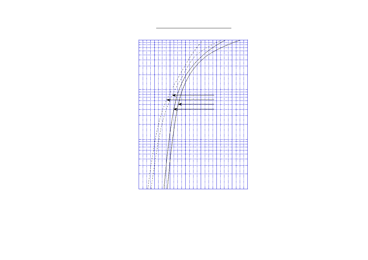
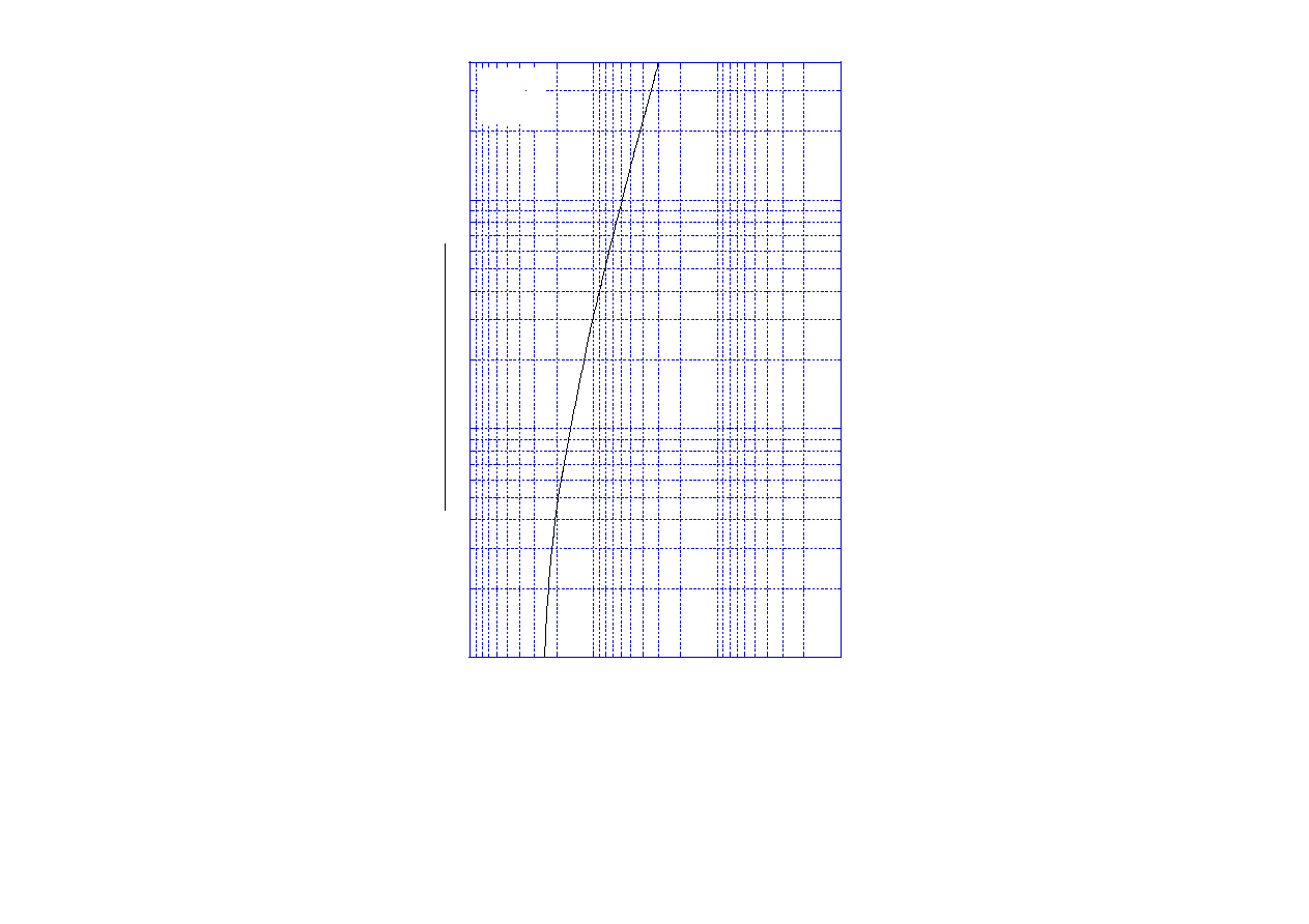
Forward Voltage
V
F
I
F
=15A, Pulse measurement, Rating of per diode
Max 0.61
V
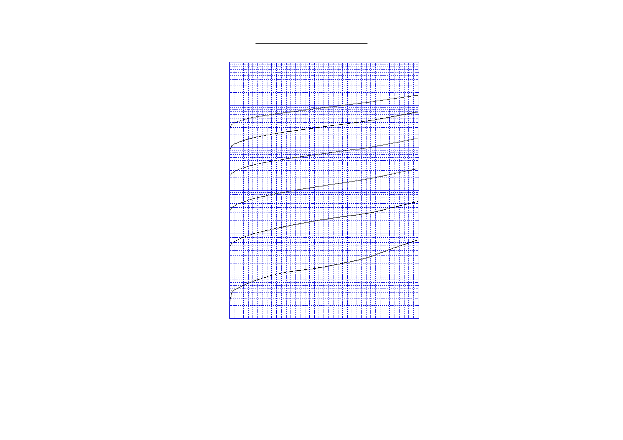
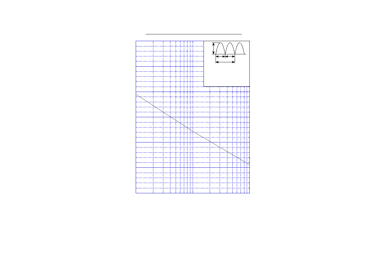
Reverse Current
I
R
V
R
=V
RM,
Pulse measurement, Rating of per diode
Max 0.7
mA
Junction Capacitance
Cj
f=1MHz, V
R
=10V, Rating of per diode
Typ 560
pF
Thermal Resistance
Æjc
junction to case
Max 1.6
/W
0
100
200
300
400
500
600
1
10
100
2
5
20
50
DF30JC4
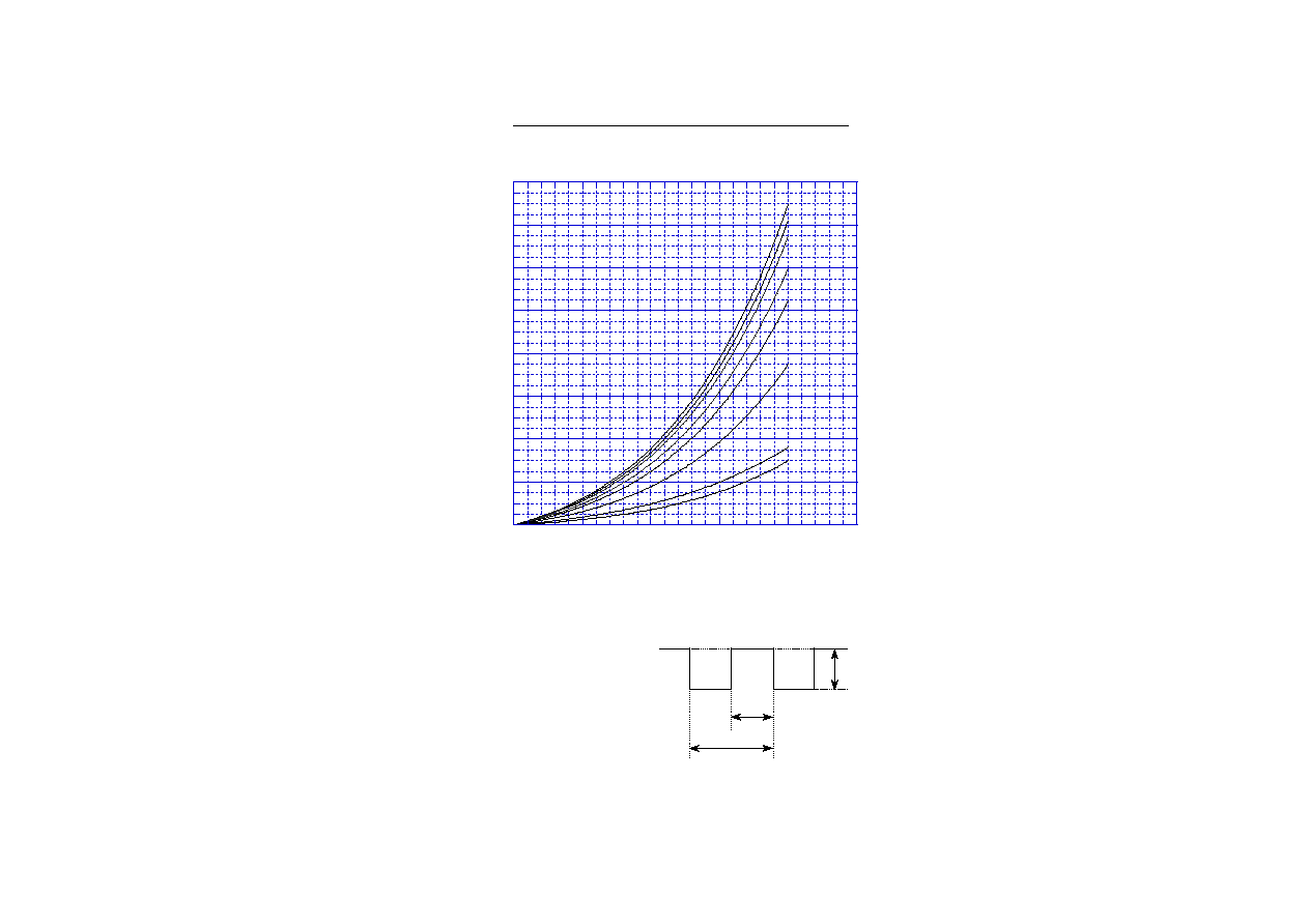
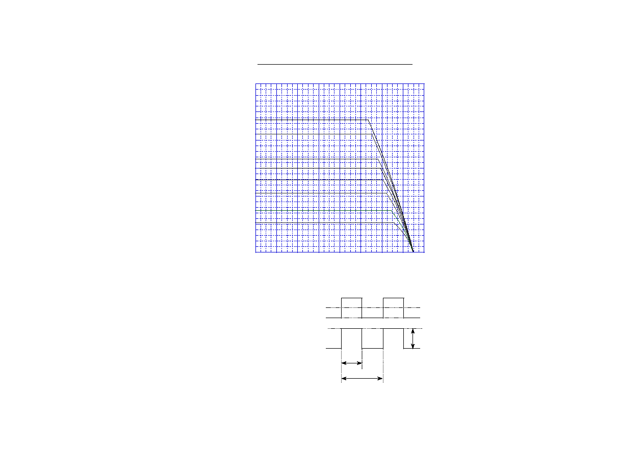
Peak Surge Forward Capability
I
FS
M
[A]
P
eak
S
u
r
g
e F
o
r
w
ar
d
C
u
r
r
e
n
t
Number of Cycles [cycle]
I
FS
M
10ms 10ms
1 cycle
non-repetitive,
sine wave,
Tj=25°C before
surge current is applied