OSD PROCESSOR FOR MONITORS S5D2501F
1
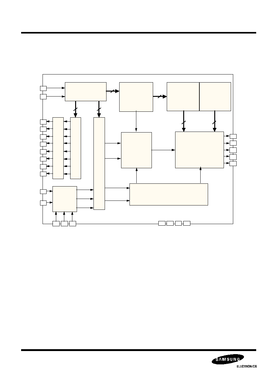
OVERVIEW
The S5D2501F is used to display some characters or symbols
on a screen of monitor. Basically, the operation is to control the
internal memory on chip and generate the R,G,B signals for
some characters or symbols. The R,G,B signals are synchro-
nized with the horizontal sync. Then the R,G,B signals are
mixed with the main video signal in the Video Amp IC.
The font data for characters or symbols are stored in the inter-
nal ROM. This stored data are accessed and controlled by the
control data from a micro controller. The control data are trans-
mitted through the I
2
C bus. All timing control signals including
the system clock are synchronized with the horizontal sync.
Therefore there is a PLL circuitry on chip.
FEATURES
·
Build in 1K-byte SRAM
·
464 ROM fonts (448 standard fonts + 16 Multi-color
fonts)
·
Full Screen Memory Architecture
·
Wide range PLL available (15 kHz -- 120 kHz)
·
Programmable vertical height of character
·
Programmable vertical and horizontal positioning
·
Character color selection up to 16 different colors
·
Programmable background color (Up to 16 colors)
·
Character blinking, bordering and shadowing
·
Color blinking
·
Character scrolling
·
Fade-in and fade-out
·
Row to row spacing control
·
Window outline and shadowing
·
Box drawing
·
Character sizing up to four times
·
8 PWM DAC channels with 8-bit resolution
·
96 MHz pixel frequency from on-chip PLL
·
I2C Protocol Data Transmission (Slave Address : BAH)
·
OSD Vertical Bouncing Auto Detect / Correction
·
Back Raster Blanking (Row Control)
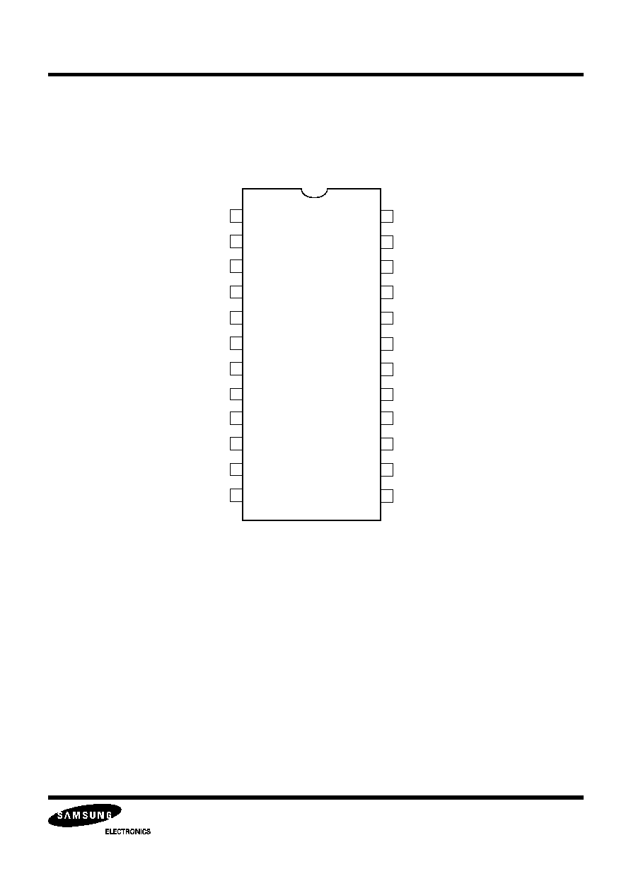
24-DIP-300
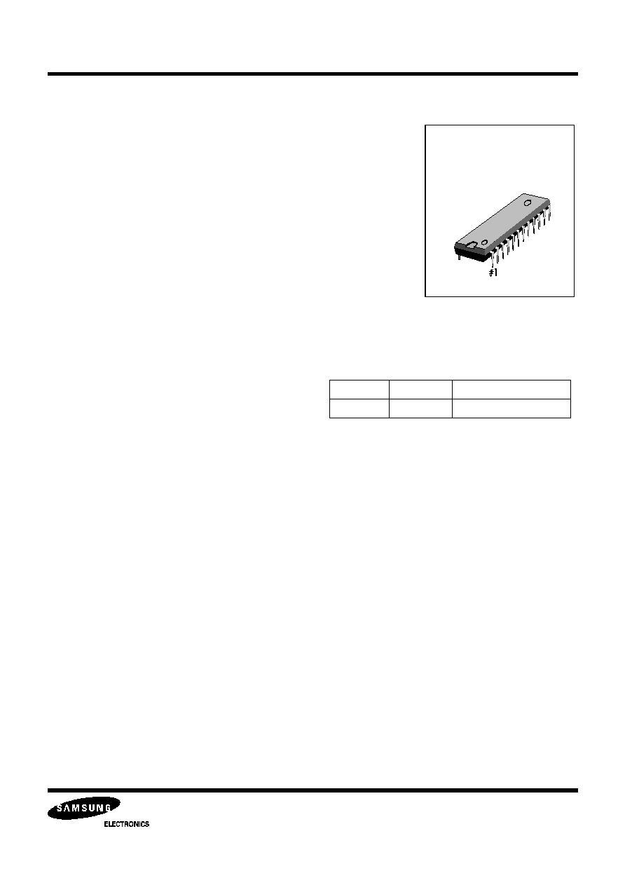
ORDERING INFORMATION
Device
Package
Operating Temperature
S5D2501F 24-DIP-300
0
°
C
-- 70
°
C
S5D2501F
OSD PROCESSOR FOR MONITORS
4
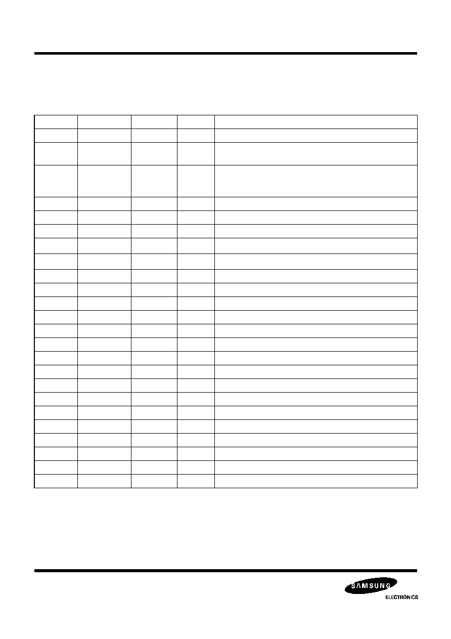
PIN DESCRIPTIONS
Table 1. Pin Descriptions
Pin No.
Signal
Active
I/O
Description
1
VSS_A
-
-
Ground (Analog Part)
2
VCO_IN
-
Input
This voltage is generated at the external loop filter and
goes into the input stage of the VCO.
3
VREF1
-
Input
1.26 V DC Voltage from the Bandgap Reference.
Connected to ground through a resistor to make internal
reference current (Typical 36 k
for 27
µ
A)
4
VREF
-
Input
Bandgap Reference Voltage (Typical 1.26 V)
5
VDD_A
-
-
+5 V Supply Voltage for Analog Part
6
HFLB
Low
Input
Horizontal Flyback Signal
7
SDA
-
In/Out
Serial Data (I
2
C)
8
SCL
-
In/Out
Serial Clock (I
2
C)
9
PWM 0
-
Output
PWM DAC 0 Output
10
PWM 1
-
Output
PWM DAC 1 Output
11
PWM 2
-
Output
PWM DAC 2 Output
12
PWM 3
-
Output
PWM DAC 3 Output
13
PWM 4
-
Output
PWM DAC 4 Output
14
PWM 5
-
Output
PWM DAC 5 Output
15
PWM 6
-
Output
PWM DAC 6 Output
16
PWM 7
-
Output
PWM DAC 7 Output
17
VFLB
Low
Input
Vertical Flyback Signal
18
VSS_D
-
-
Ground for Digital Part
19
FBLK
-
Output
Fast Blank Signal
20
B_OUT
-
Output
Video Signal Output (B)
21
G_OUT
-
Output
Video Signal Output (G)
22
R_OUT
-
Output
Video Signal Output (R)
23
INT
-
Output
Intensity Signal Output
24
VDD_D
-
-
+5 V Supply Voltage for Dogital Part