 | –≠–ª–µ–∫—Ç—Ä–æ–Ω–Ω—ã–π –∫–æ–º–ø–æ–Ω–µ–Ω—Ç: S3P8095 | –°–∫–∞—á–∞—Ç—å:  PDF PDF  ZIP ZIP |
S3C8095/P8095
PRODUCT OVERVIEW
1-1
1
PRODUCT OVERVIEW
S3C8-SERIES MICROCONTROLLERS
Samsung's S3C8 series of 8-bit single-chip CMOS microcontrollers offers a fast and efficient CPU, a wide range
of integrated peripherals, and various mask-programmable ROM sizes. Important CPU features include:
-- Efficient register-oriented architecture
-- Selectable CPU clock sources
-- Idle and Stop power-down mode release by interrupt
-- Built-in basic timer with watchdog function
A sophisticated interrupt structure recognizes up to eight interrupt levels. Each level can have one or more
interrupt sources and vectors. Fast interrupt processing (within a minimum six CPU clocks) can be assigned to
specific interrupt levels.
S3C8095/P8095 MICROCONTROLLER
The S3C8095/P8095 single-chip CMOS
microcontroller is fabricated using a highly advanced
CMOS process and is based on Samsung's newest
CPU architecture.
The S3C8095 is the microcontroller which has 16-
Kbytes mask-programmable ROM.
The S3P8095 is the microcontroller which has 16-
Kbytes one-time-programmable EPROM.
Using a proven modular design approach, Samsung
engineers developed the S3C8095/P8095 by
integrating the following peripheral modules with the
powerful SAM87 core:
-- Four programmable I/O ports, including three
8-bit ports and one 2-bit port, for a total of 26
pins.
-- Twelve bit-programmable pins for external
interrupts.
-- One 8-bit basic timer for oscillation stabilization
and watchdog functions (system reset).
-- One 8-bit timer/counter and one 16-bit
timer/counter with selectable operating modes.
-- One 8-bit counter with auto-reload function and
one-shot or repeat control.
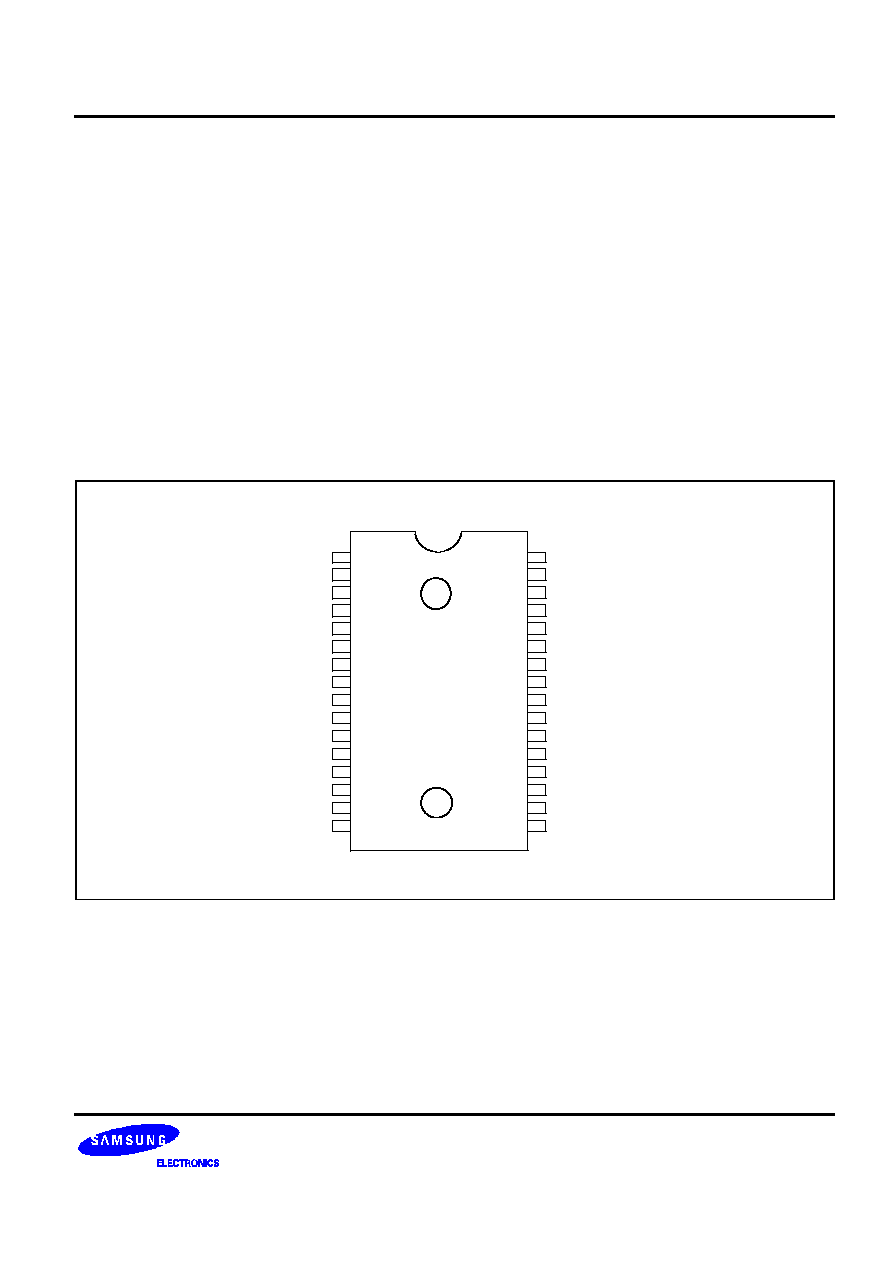
The S3C8095 is a versatile general-purpose
microcontroller. It is currently available in a 32-pin
SOP and SDIP package.
Figure 1-1. S3C8095 Microcontroller

PRODUCT OVERVIEW
S3C8095/P8095
1-2
FEATURES
CPU
∑
SAM87 CPU core
Memory
∑
16K-byte internal program memory (ROM)
∑
317-byte internal register file
Instruction Set
∑
78 instructions
∑
IDLE and STOP instructions added for power-
down modes
Instruction Execution Time
∑
750 ns at 8-MHz f
OSC
(minimum)
Interrupts
∑
Six interrupt levels and 18 interrupt sources
∑
15 vectors (14 sources have a dedicated vector
address and four sources share a single vector)
∑
Fast interrupt processing feature (for one
selected interrupt level)
I/O Ports
∑
Three 8-bit I/O ports (P0≠P2) and one 2-bit port
(P3) for a total of 26 bit-programmable pins
∑
Twelve input pins for external interrupts
Timers and Timer/Counters
∑
One programmable 8-bit basic timer (BT) for
oscillation stabilization control or watchdog timer
(software reset) function
∑
One 8-bit timer/counter (Timer 0) with three
operating modes; Interval, Capture and PWM
∑
One 16-bit timer/counter (Timer 1) with two
operating modes; Interval and Capture
Carrier Frequency Generator
∑
One 8-bit counter with auto-reload function and
one-shot or repeat control (Counter A)
Operating Temperature Range
∑
≠ 20
∞
C to + 85
∞
C
Operating Voltage Range
∑
2.0 V to 5.5 V at 4 MHz f
OSC
∑
2.4 V to 5.5 V at 8 MHz f
OSC
Package Type
∑
32-pin SOP
∑
32-pin SDIP
S3C8095/P8095
PRODUCT OVERVIEW
1-3
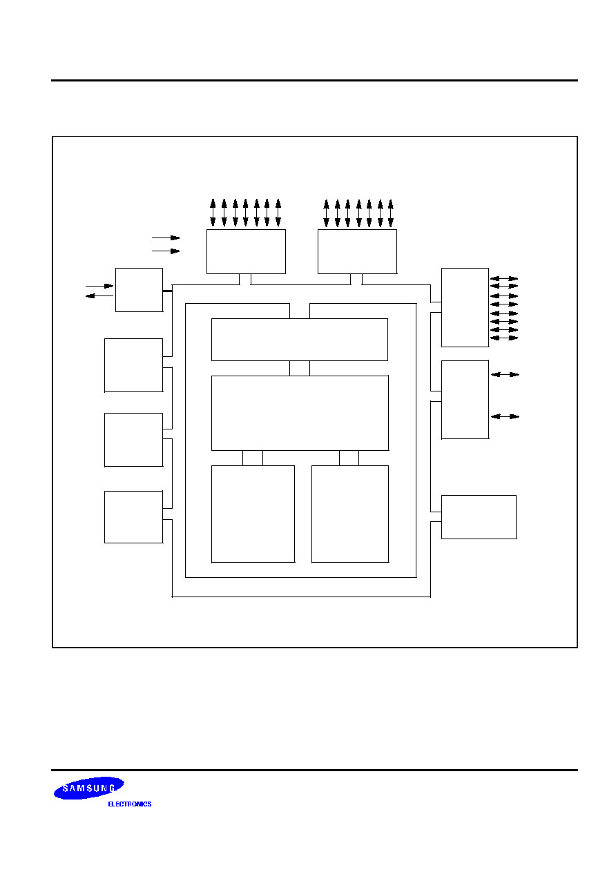
BLOCK DIAGRAM
I/O PORT and INTERRUPT
CONTROL
SAM8 CPU
X
IN
X
OUT
INTERNAL BUS
8-BIT
BASIC
TIMER
PORT2
16-KB ROM
317-BYTES
REGISTER
FILE
P2.0≠P2.3
(INT5≠INT8)
P2.4≠P2.7
PORT 0
P1.0≠P1.7
PORT 1
8-BIT
TIMER/
COUNTER
16-BIT
TIMER/
COUNTER
CARRIER
GENERATOR
(COUNTER A)
RESET
TEST
PORT 3
P3.1/REM/T0CK
P3.0/T0PWM/
T0CAP/T1CAP
P0.0≠P0.7
(INT0≠INT4)
MAIN
OSC
Figure 1-2. Block Diagram
PRODUCT OVERVIEW
S3C8095/P8095
1-4
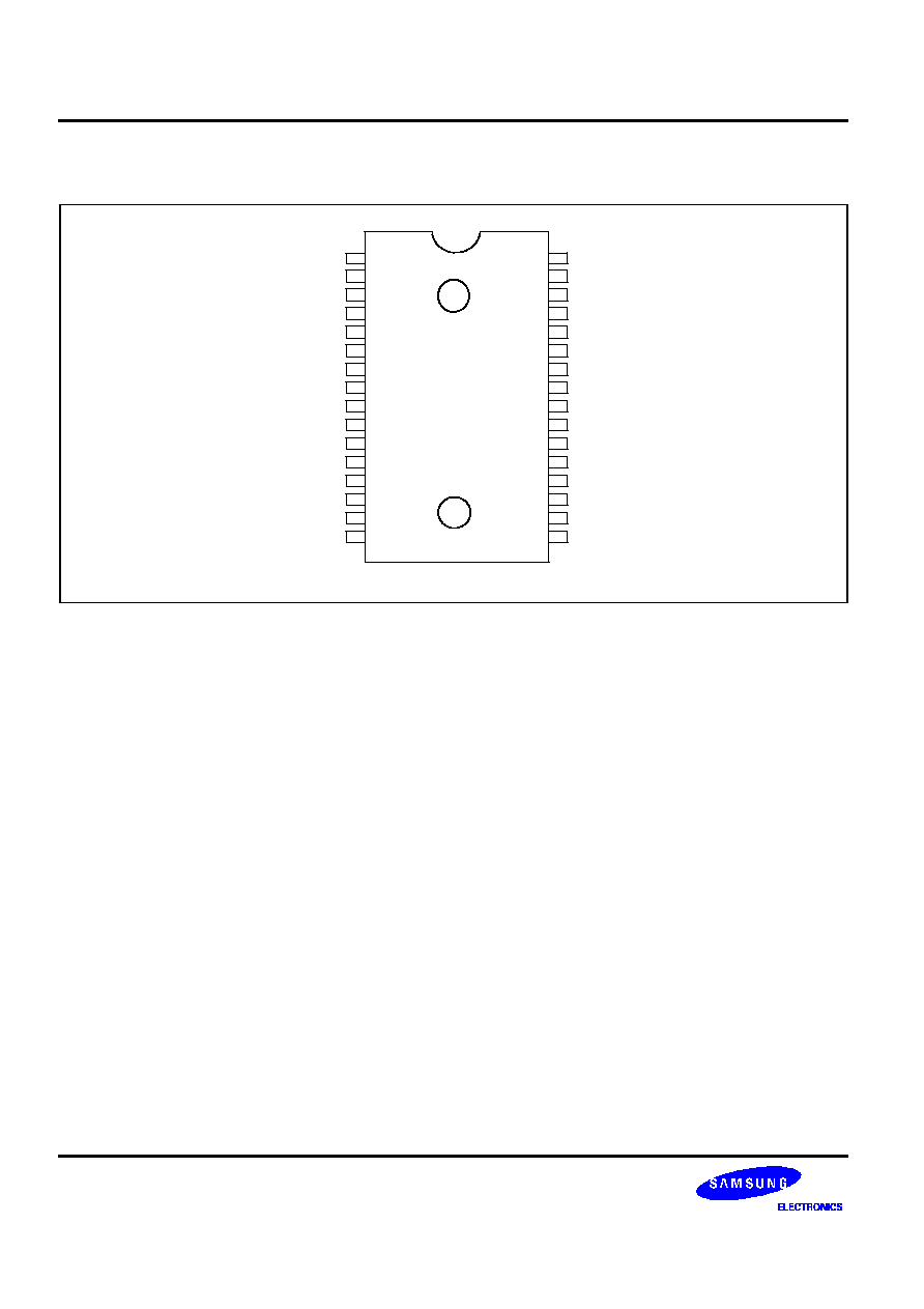
PIN ASSIGNMENTS
V
SS
X
IN
X
OUT
TEST
P2.0 / INT5
P2.1 / INT6
P2.2 / INT7
P2.3 / INT8
P0.0 / INT0
P0.1 / INT1
P0.2 / INT2
P0.3 / INT3
P0.4 / INT4
P0.5 / INT4
P0.6 / INT4
P0.7 / INT4
V
DD
P3.1 / REM / T0CK
P3.0 / T0PWM / T0CAP / T1CAP
P2.7
P2.6
P2.5
P2.4
P1.7
P1.6
P1.5
P1.4
P1.3
P1.2
P1.1
P1.0
1
2
3
4
5
6
7
8
9
10
11
12
13
14
15
16
32
31
30
29
28
27
26
25
24
23
22
21
20
19
18
17
S3C8095
32-SOP/SDIP
(Top View)
RESET
Figure 1-3. Pin Assignment Diagram (32-Pin SOP/SDIP Package)
S3C8095/P8095
PRODUCT OVERVIEW
1-5
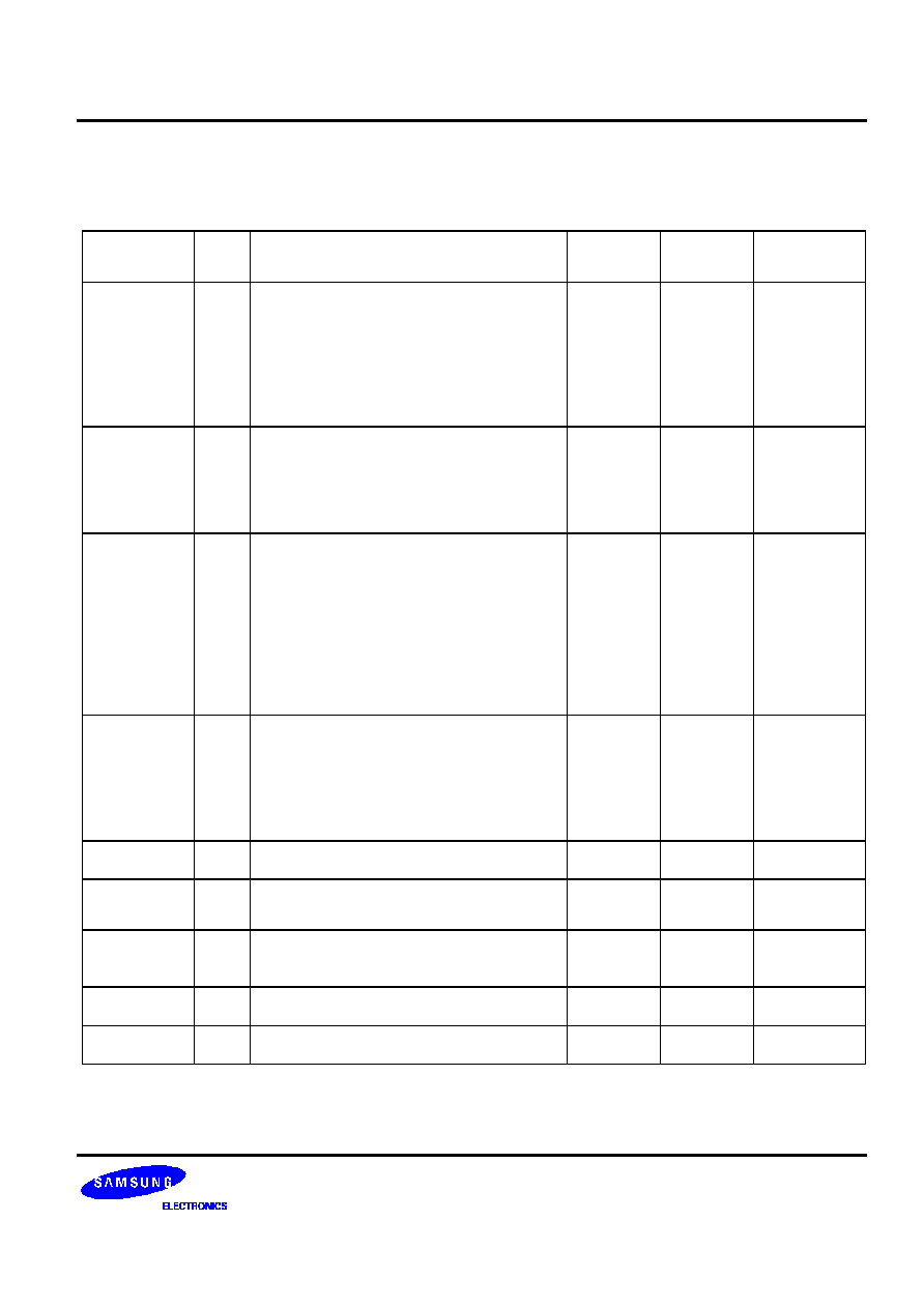
PIN DESCRIPTIONS
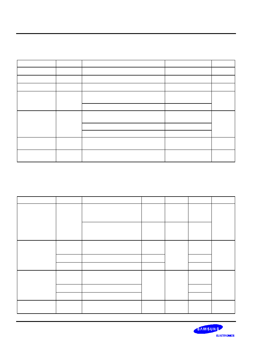
Table 1-1. Pin Descriptions
Pin
Names
Pin
Type
Pin
Description
Circuit
Type
Pin No.
Shared
Functions
P0.0≠P0.7
I/O
I/O port with bit-programmable pins.
Configurable to input or push-pull output
mode. Pull-up resistors are assignable by
software. Pins can be assigned individually
as external interrupt inputs with noise filters,
interrupt enable/ disable, and interrupt
pending control.
1
9≠16
INT0≠INT4
P1.0≠P1.7
I/O
I/O port with bit-programmable pins.
Configurable to Schmitt trigger input mode
or output mode. Pin circuits are either push-
pull or n-channel open-drain type. Pull-up
resistors are assignable by software.
3
17≠24
≠
P2.0≠P2.3
P2.4≠P2.7
I/O
General-purpose I/O port with bit-
programmable pins. Configurable to
Schmitt trigger input mode, push-pull output
mode, or n-channel open-drain output
mode. Pull-up resistors are assignable by
software. Lower nibble pins, P2.3≠P2.0, can
be assigned as external interrupt inputs with
noise filters, interrupt enable/disable, and
interrupt pending control.
2
3
5≠8,
25≠28
INT5≠INT8
≠
P3.0
P3.1
I/O
2-bit I/O port with bit-programmable pins.
Configurable to Schmitt trigger input mode,
push-pull output mode, or n-channel open-
drain output mode. Pull-up resistors are
assignable by software. The two port 3 pins
have high current drive capability.
4
29
30
T0PWM/
T0CAP/
T1CAP/
REM/T0CK
X
IN
, X
OUT
≠
System clock input and output pins
≠
2, 3
≠
RESET
I
System reset signal input pin with schmitt
trigger circuit.
5
31
≠
TEST
I
Test signal input pin (for factory use only;
must be connected to V
SS
).
≠
4
≠
V
DD
≠
Power supply input pin
≠
32
≠
V
SS
≠
Ground pin
≠
1
≠
PRODUCT OVERVIEW
S3C8095/P8095
1-6
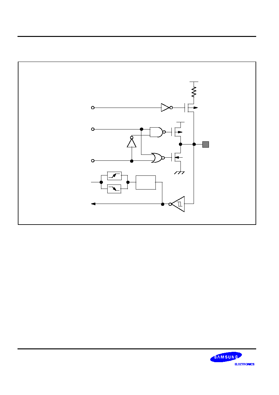
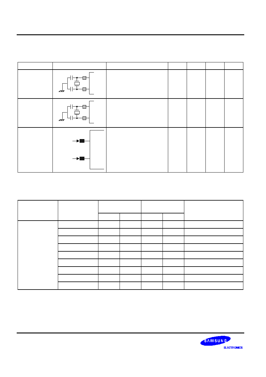
PIN CIRCUITS
PULL-UP
RESISTOR
(Typical
50
)
V
DD
INPUT /
OUTPUT
V
SS
DATA
PULL-UP
ENABLE
NORMAL
INPUT
OUTPUT
DISABLE
V
DD
NOISE
FILTER
INTERRUPT INPUT
IRQ6,7 (INT0 -4)
Figure 1-4. Pin Circuit Type 1 (Port 0)
S3C8095/P8095
PRODUCT OVERVIEW
1-7
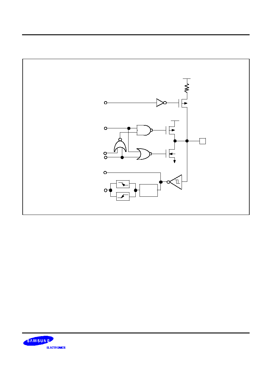
PIN CIRCUITS
(Cont.)
IN / OUT
V
SS
V
DD
IRQ5 (INT5-8)
NOISE
FILTER
RESISTOR
V
DD
ENABLE
(Typical 50
)
PULL-UP
PULL-UP
NORMAL INPUT
EXTERNAL
INTERRUPT
DATA
OPEN-DRAIN
OUTPUT DISABLE
Figure 1-5. Pin Circuit Type 2 (Ports 2.0≠2.3)
PRODUCT OVERVIEW
S3C8095/P8095
1-8
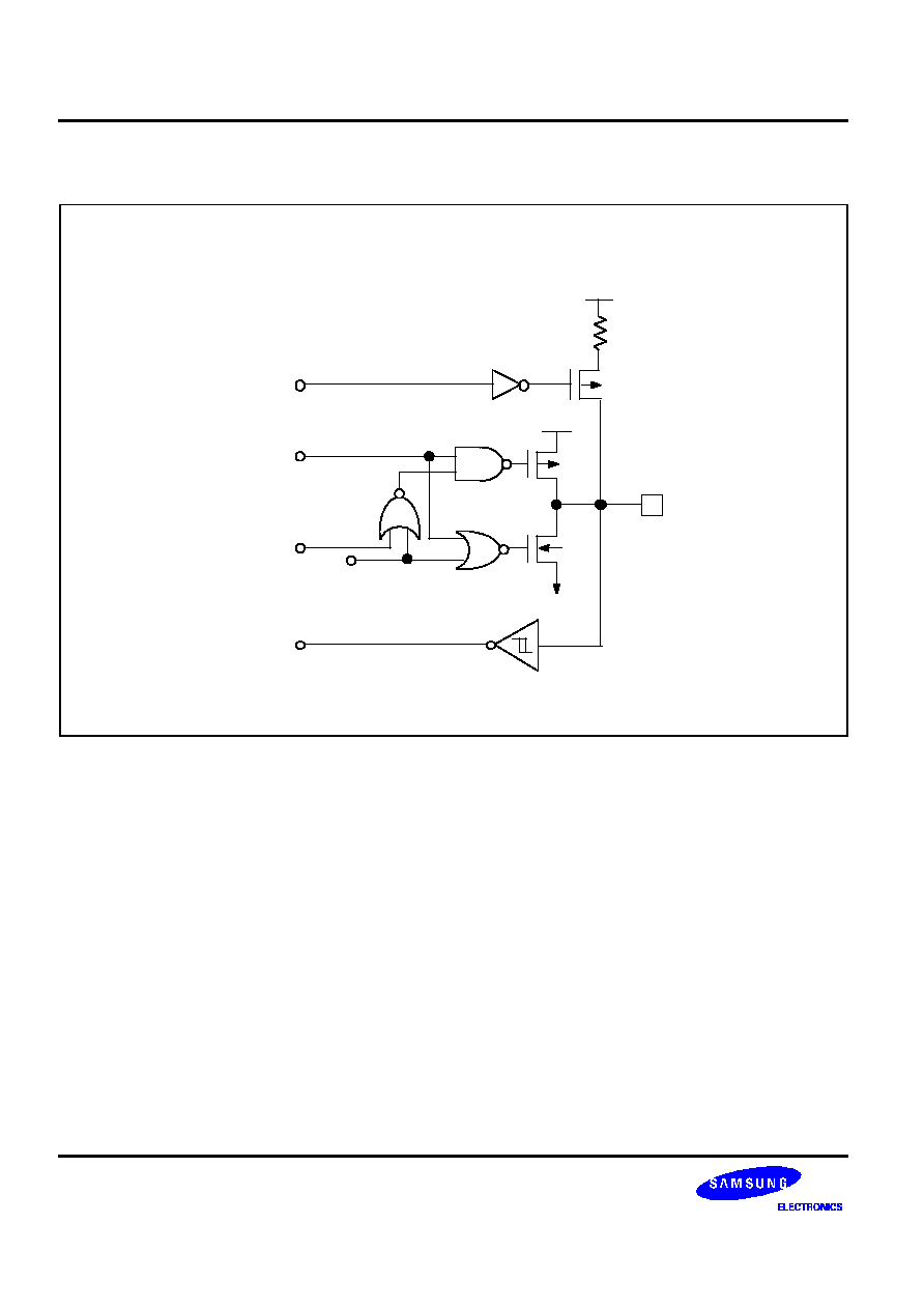
PIN CIRCUITS (
Cont
.)
PULL-UP
RESISTOR
(Typical 50
)
DATA
V
DD
IN / OUT
PULL-UP
ENABLE
V
SS
OPEN-
DRAIN
OUTPUT
DISABLE
V
DD
NORMAL INPUT
Figure 1-6. Pin Circuit Type 3 (Ports 1 and P2.4≠P2.7)
S3C8095/P8095
PRODUCT OVERVIEW
1-9
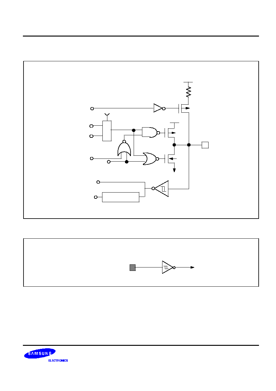
PIN CIRCUITS
(Cont.)
PULL-UP
RESISTOR
(
Typical
50
)
V
DD
IN / OUT
PULL-UP
ENABLE
V
SS
OPEN-
DRAIN
OUTPUT
DISABLE
V
DD
NORMAL INPUT
DATA
PORT 3
DATA
SELECT
ALTERNATIVE
OUTPUT
M
U
X
NOISE FILTER
ALTERNATIVE
INPUT
Figure 1-7. Pin Circuit Type 4 (Port 3)
RESET
Figure 1-8. Pin Circuit Type 5 (
R
RESET
ESET
)
S3C8095/P8095
S3P8095 OTP
13-1
13
S3P8095 OTP
OVERVIEW
The S3P8095 single-chip CMOS microcontroller is the OTP (One Time Programmable)
version of the S3C8095
microcontroller. It has an on-chip EPROM instead of masked ROM.
The S3P8095 is fully compatible with the S3C8095, both in function and in pin configuration. Because of its
simple programming requirements, the S3P8095 is ideal for use as an evaluation chip for the S3C8095.
V
SS
X
IN
X
OUT
MODE/TEST
PGM
PGM
/P2.0 / INT5
MEM_
REG
REG
/P2.1 / INT6
A8/P2.2 / INT7
A9/P2.3 / INT8
A0/P0.0 / INT0
A1/P0.1 / INT1
A2/P0.2 / INT2
A3/P0.3 / INT3
A4/P0.4 / INT4
A5/P0.5 / INT4
A6/P0.6 / INT4
A7/P0.7 / INT4
V
DD
P3.1/REM/T0CK/
CE
CE
P3.0/
OE
OE
P2.7/ A13
P2.6/ A12
P2.5/ A11
P2.4/ A10
P1.7/ D7
P1.6/ D6
P1.5/ D5
P1.4/ D4
P1.3/ D3
P1.2/ D2
P1.1/ D1
P1.0/ D0
1
2
3
4
5
6
7
8
9
10
11
12
13
14
15
16
32
31
30
29
28
27
26
25
24
23
22
21
20
19
18
17
S3P8095
32-SOP/SDIP
(Top View)
RESET/
V
PP
Figure 13-1. S3P8095 Pin Assignments
S3P8095 OTP
S3C8095/P8095
13-2
Table 13≠1. Pin Descriptions used to read/write the EPROM
Pin Name
Pin No.
I/O
Function
A0 - A13
7 - 16, 25 - 28
O
Address lines to read/write EPROM
D0 - D7
17 - 24
I/O
8-bit data input/output lines to read/write EPROM
MODE
4
--
Select EPROM mode.
CE
30
I
Chip enable (Connect to V
SS, when read/write EPROM)
OE
29
I
Output enable
PGM
5
I
EPROM Program enable
MEM_
REG
6
I
Select Memory space of EPROM
V
DD
32
≠
Supply voltage (normally 5 V)
V
PP
31
≠
EPROM Program/Verify voltage (normally 12.5 V)
V
SS
1
≠
GROUND
X
IN
2
≠
System Clock input pin
X
OUT
3
≠
System Clock output pin
CHARACTERISTICS OF EPROM OPERATION
When +12.5 V is supplied to V
PP
and MODE pins of the S3P8095, the EPROM programming mode is entered.
The operating mode (read, write) is selected according to the input signals to the pins listed in Table2 as below.
Table 13-2. Operating Mode Selection Criteria
V
DD
MODE
V
PP
PGM
PGM
MEM
OE
OE
Mode
5 V
V
PP
12.5 V
1
1
0
READ
0
1
1
PROGRAM
1
1
0
PROGRAM VERIFY
NOTE: "0" means Low level; "1" means High level.
S3C8095/P8095
S3P8095 OTP
13-3
MODE
OE
OE
D7 - D0
A13 - A0
tOED
tACC
tOEW
tOEH
12.5V
Figure 13-2. OTP Read Timing
Table 13-3. OTP Read characteristics
(T
A
= 25
∞
C ± 5
∞
C, V
DD
= 5 V ± 5 %, V
PP
= 12.5 V ± 0.25V)
Parameter
Symbol
Min
Typ
Max
Units
Address to Output Delay
t
ACC
--
--
75
ns
OE
to Address Delay
t
OED
0
--
--
OE
Pulse Width
t
OEW
75
--
--
Output hold from
OE
whichever occurs first
t
OEH
0
--
--
S3P8095 OTP
S3C8095/P8095
13-4
PGM
OE
OE
D7 - D0
A13 - A0
tOEW
tOE
tOEH
tPW
tVS
tDS
Data In Stable
Data Out Valid
PROGRAM VERIFY
PROGRAM
tDH
MODE
Figure 13-3. Program Memory Write Timing
Table 13-4. OTP Program/Program Verify Characteristics
(T
A
= 25
∞
C ± 5
∞
C, V
DD
= 5 V ± 5 %, V
PP
= 12.5 V ± 0.25V)
Parameter
Symbol
Min
Typ
Max
Units
V
PP
Setup Time
t
VS
--
2
--
µs
Data Setup Time
t
DS
--
2
--
Data Hold Time
t
DH
--
2
--
PGM
Pulse Width
t
PW
--
300
500
Data Valid from
OE
t
OE
75
--
--
ns
OE
Pulse Width
t
OEW
75
--
--
Output Enable to Output Float
Delay
t
OEH
0
--
130
S3C8095/P8095
S3P8095 OTP
13-5
START
Address = First Location
V
DD
= 5 V, V
PP
= 12.5 V
X = 0
Program One 1ms Pulse
Increment X
V
DD
= V
PP
= 5V
Device Passed
Compare All byte
X = 10
Verify 1 Byte
Last Address
Verify Byte
Device Failed
Increment Address
YES
FAIL
NO
FAIL
PASS
NO
YES
PASS
FAIL
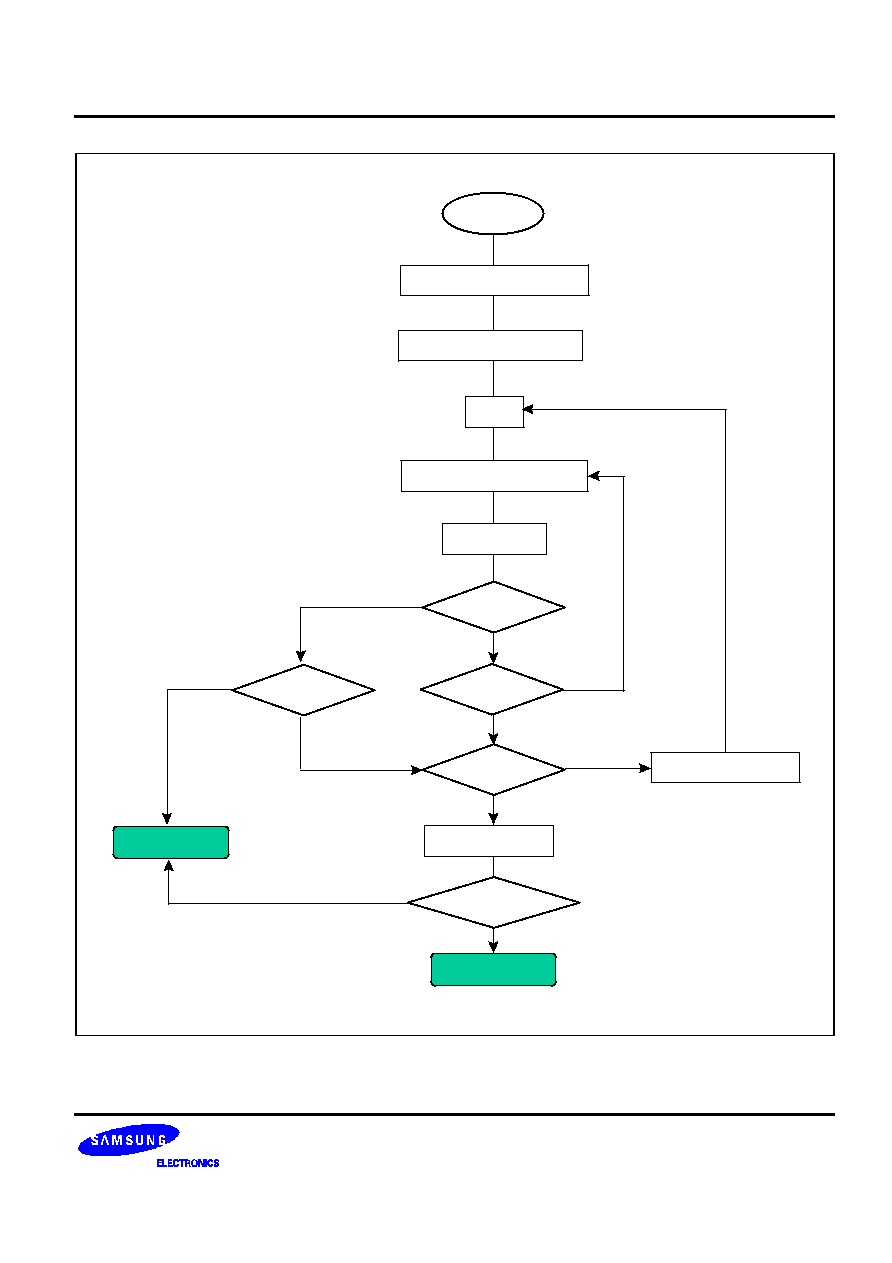
Figure 13-4. OTP Programming Algorithm

S3C8095/P8095
ELECTRICAL DATA
14-1
14
ELECTRICAL DATA
OVERVIEW
In this section, S3C8095/P8095 electrical characteristics are presented in tables and graphs. The information is
arranged in the following order:
--
Absolute maximum ratings
--
D.C. electrical characteristics
--
Data retention supply voltage in Stop mode
--
Stop mode release timing when initiated by an external interrupt
--
Stop mode release timing when initiated by a Reset
--
I/O capacitance
--
A.C. electrical characteristics
--
Input timing for external interrupts (port 0, P2.3≠P2.0)
--
Input timing for
RESET
--
Oscillation characteristics
--
Oscillation stabilization time
ELECTRICAL DATA
S3C8095/P8095
14-2
Table 14-1. Absolute Maximum Ratings
(T
A
= 25
∞
C)
Parameter
Symbol
Conditions
Rating
Unit
Supply voltage
V
DD
≠
≠ 0.3 to + 6.5
V
Input voltage
V
IN
≠
≠ 0.3 to
V
DD
+ 0.3
V
Output voltage
V
O
All output pins
≠ 0.3 to V
DD
+ 0.3
V
Output current
High
I
OH
One I/O pin active
≠ 18
mA
All I/O pins active
≠ 60
Output current
Low
I
OL
One I/O pin active
+ 30
mA
Total pin current for ports 0, 1, and 2
+ 100
Total pin current for port 3
+ 20
Operating
temperature
T
A
≠
≠ 20 to + 85
∞
C
Storage
temperature
T
STG
≠
≠ 65 to + 150
∞
C
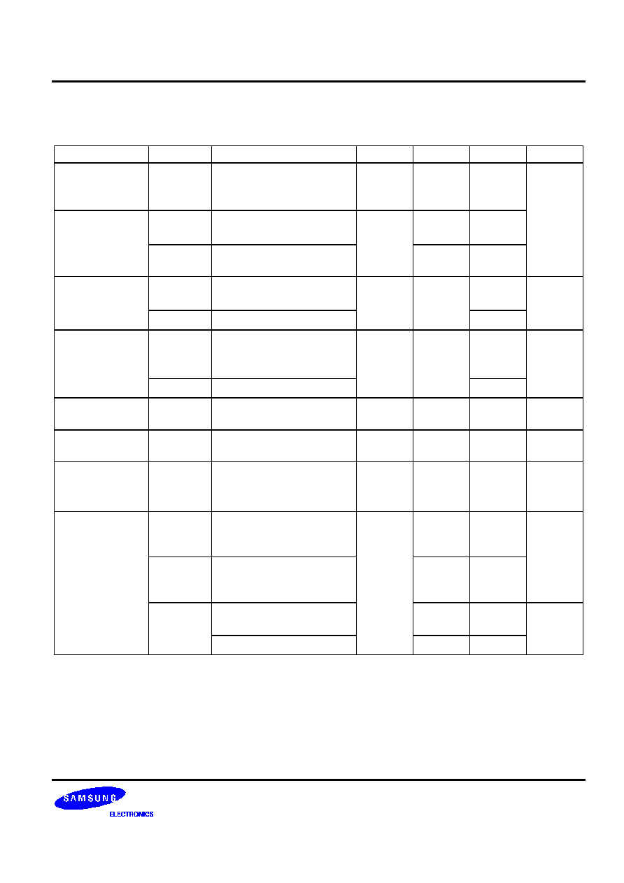
Table 14-2. D.C. Electrical Characteristics
(T
A
= ≠ 20
∞
C to + 85
∞
C, V
DD
= 2.0 V to 5.5 V)
Parameter
Symbol
Conditions
Min
Typ
Max
Unit
Operating Voltage
V
DD
f
OSC
= 8 MHz
(Instruction clock = 1.33
MHz)
2.4
--
5.5
V
f
OSC
= 4 MHz
(Instruction clock = 0.67
MHz)
2.0
--
5.5
Input High
voltage
V
IH1
All input pins except V
IH2
and V
IH3
0.8 V
DD
≠
V
DD
V
V
IH2
RESET
0.95 V
DD
V
DD
V
IH3
X
IN
V
DD
≠ 0.3
V
DD
Input Low voltage
V
IL1
All input pins except V
IL2
and V
IL3
0
≠
0.2 V
DD
V
V
IL2
RESET
0.3 V
DD
V
IL3
X
IN
0.3
Output High
voltage
V
OH1
V
DD
= 3.0 V IOH = ≠ 7 mA
Port 3 only
V
DD
≠ 2.0
≠
≠
V
S3C8095/P8095
ELECTRICAL DATA
14-3
Table 14-2. D.C. Electrical Characteristics (Continued)
(T
A
= ≠ 20
∞
C to + 85
∞
C, V
DD
= 2.0 V to 5.5 V)
Parameter
Symbol
Conditions
Min
Typ
Max
Unit
Output High
voltage
V
OH2
V
DD
= 3.0 V
I
OH
= ≠ 200
µ
A
All output pins except port 3
V
DD
≠ 1.0
≠
≠
V
Output Low
voltage
V
OL1
V
DD
= 3.0 V
I
OL
= 1.5 mA, port 3 only
≠
0.3
0.6
V
OL2
I
OL
= 1 mA
Ports 0, 1 and 2
0.4
1.0
Input High
leakage current
I
LIH1
V
IN
= V
DD
; all input pins
except X
IN
and X
OUT
≠
≠
1
µA
I
LIH2
V
IN
= V
DD
, X
IN
and X
OUT
20
Input Low
leakage current
I
LIL1
V
IN
= 0 V; all input pins
except X
IN
, X
OUT
, and
RESET
≠
≠
≠ 1
µA
I
LIL2
V
IN
= 0 V, X
IN
and X
OUT
≠ 20
Output High
leakage current
I
LOH
V
OUT
= V
DD
All output pins
≠
≠
1
µA
Output Low
leakage current
I
LOL
V
OUT
= 0 V
All output pins
≠
≠
≠ 1
µA
Pull-up resistors
R
L1
V
IN
= 0 V; T
A
= 25
∞
C
V
DD
= 5.0 V
±
10 %
Ports 0≠3
30
50
100
K
Supply current
(See Note)
I
DD1
Operating mode;
V
DD
= 5.0 V
±
10 %
4-MHz crystal
≠
4.5
9
mA
I
DD2
Idle mode;
V
DD
= 5.0 V
±
10 %
4-MHz crystal
1.6
3
I
DD3
Stop mode;
V
DD
= 5.0 V
±
10 %
0.3
3
µA
V
DD
= 3.6 V
0.1
1
NOTE: Supply current does not include current drawn through internal pull-up resistors or external output current loads.
ELECTRICAL DATA
S3C8095/P8095
14-4
Table 14-3. Data Retention Supply Voltage in Stop Mode
(T
A
= ≠ 20
∞
C to + 85
∞
C)
Parameter
Symbol
Conditions
Min
Typ
Max
Unit
Data retention supply
voltage
V
DDDR
≠
1.0
≠
5.5
V
Data retention supply
current
I
DDDR
V
DDDR
= 1.0 V
Stop mode
≠
≠
1
µA
V
DD
EXT
INT
EXECUTION OF
STOP INSTRUCTION
V
DDDR
DATA RETENTION MODE
STOP MODE
NORMAL
OPERATING
MODE
t
WAIT
0.2 V
DD
0.8 V
DD
IDLE MODE
(Basic Timer active)
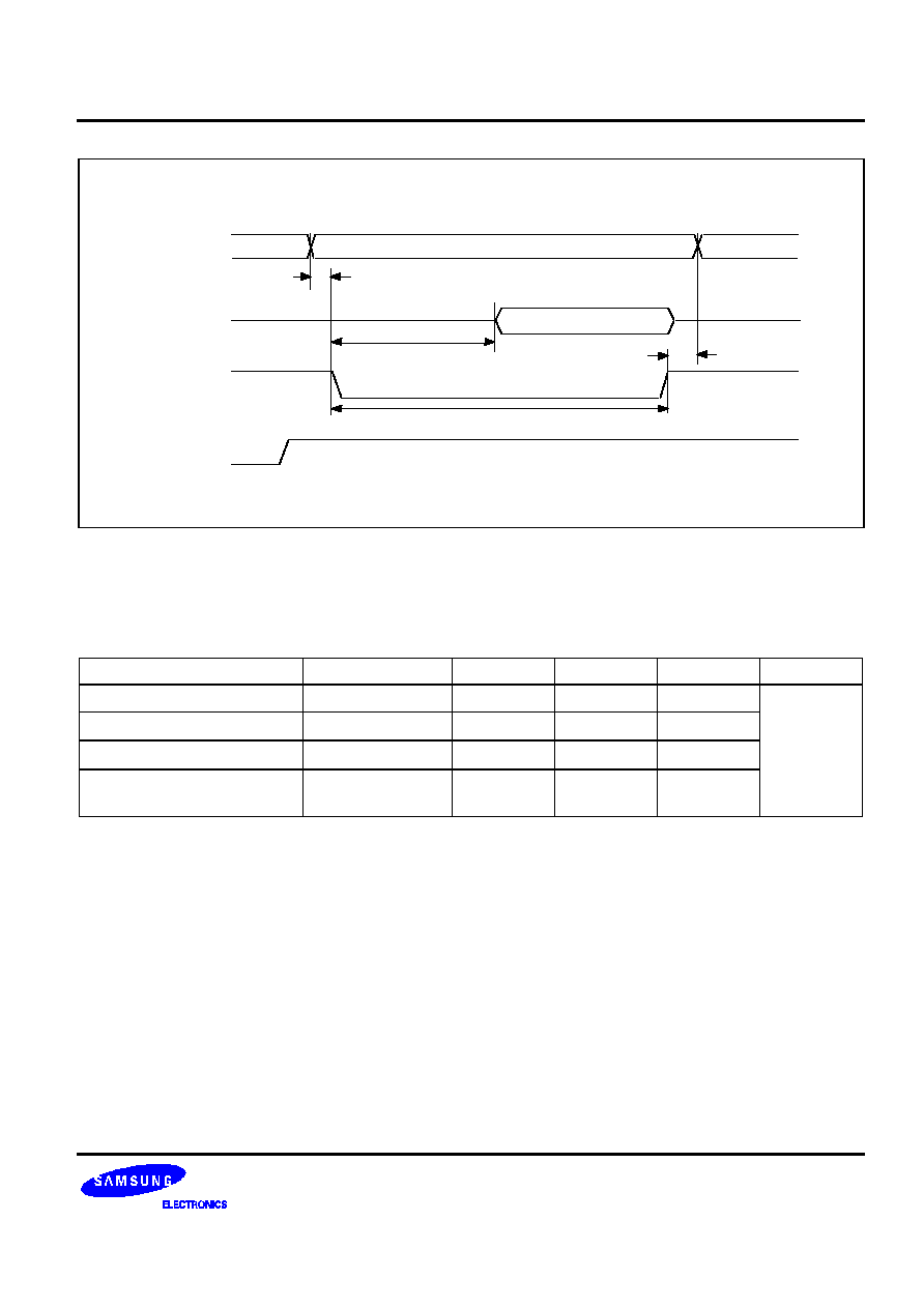
Figure 14-1. Stop Mode Release Timing When Initiated by an External Interrupt
VDD
RESET
EXECUTION OF
STOP INSTRUCTION
VDDDR
DATA RETENTION MODE
STOP MODE
NORMAL
OPERATING
MODE
tWAIT
OSCILLATION
STABILIZATION
TIME
RESET
OCCURS
Note :
tWAIT is the same as 4096 x 16 x 1/f OSC
Figure 14-2. Stop Mode Release Timing When Initiated by a Reset
S3C8095/P8095
ELECTRICAL DATA
14-5
Table 14-4. Input/Output Capacitance
(T
A
= ≠ 20
∞
C to + 85
∞
C, V
DD
=
0 V)
Parameter
Symbol
Conditions
Min
Typ
Max
Unit
Input
capacitance
C
IN
f = 1 MHz; unmeasured pins
are connected to V
SS
--
--
10
pF
Output
capacitance
C
OUT
I/O capacitance
C
IO
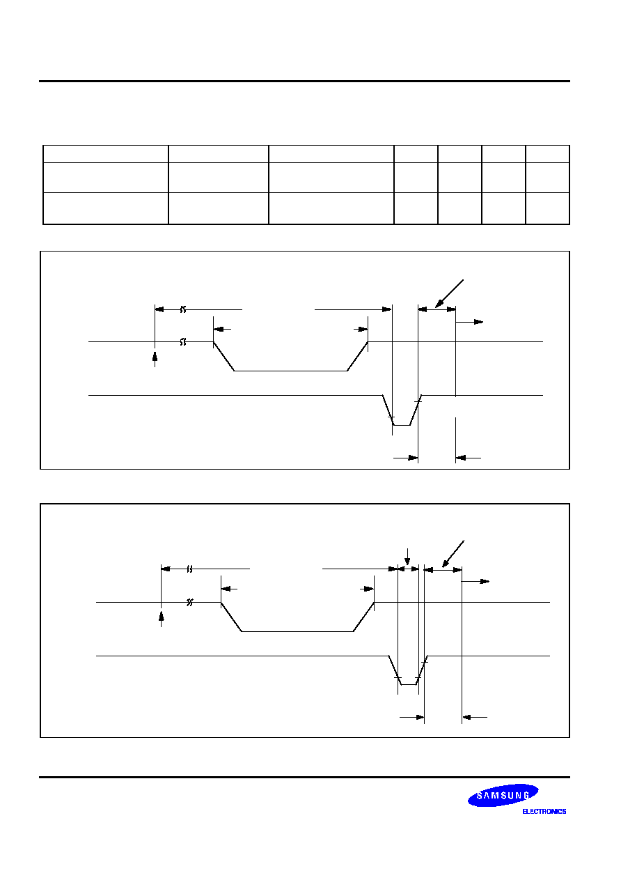
Table 14-5. A.C. Electrical Characteristics
(T
A
= ≠ 20
∞
C to + 85
∞
C)
Parameter
Symbol
Conditions
Min
Typ
Max
Unit
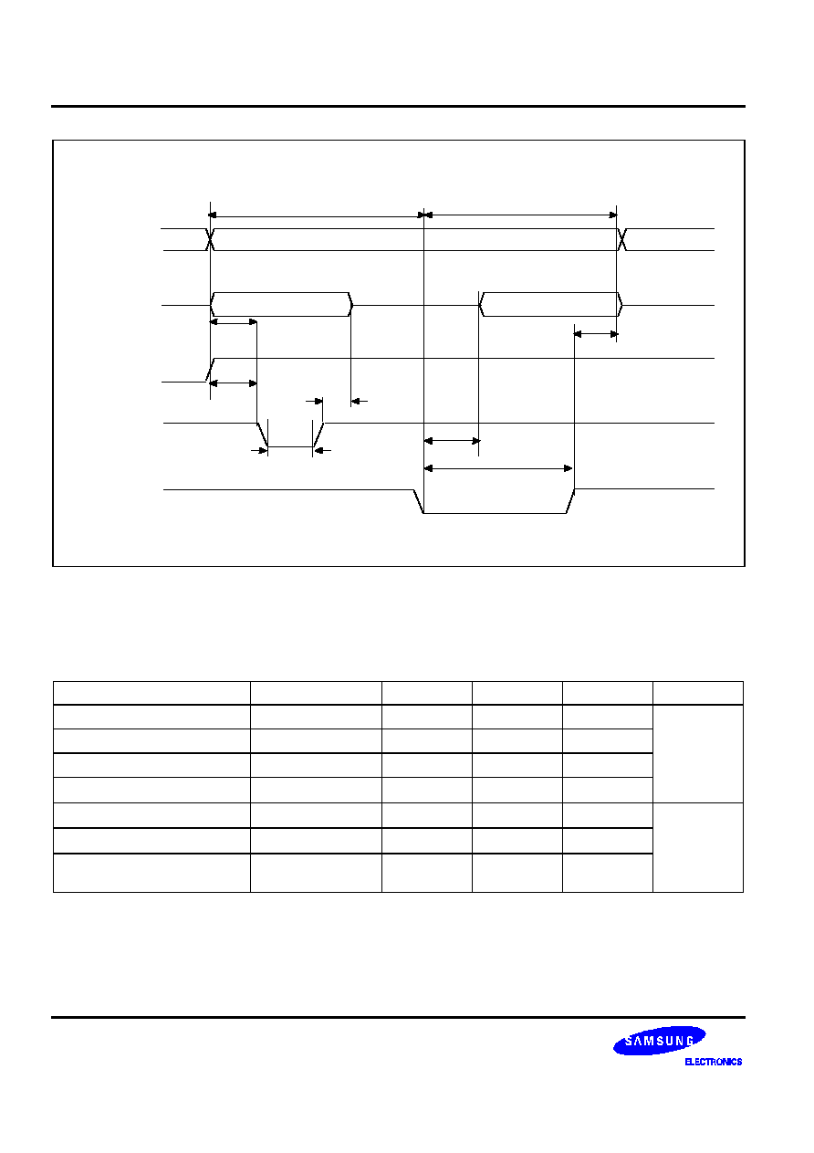
Interrupt input,
High, Low width
t
INTH
,
t
INTL
P0.0≠P0.7, P2.3≠P2.0
V
DD
= 5 V
200
300
--
ns
RESET
input Low
width
t
RSL
Input
V
DD
= 5 V
1000
--
--
t
INTL
t
INTH
0.8 V
DD
0.2 V
DD
NOTE:
The unit t
CPU
means one CPU clock period.
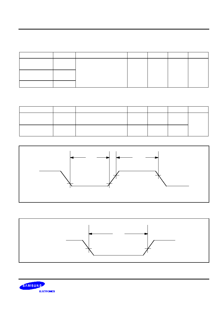
Figure 14-3. Input Timing for External Interrupts (Port 0, P2.3≠P2.0)
tRSL
0.3 V DD
RESET
Figure 14-4. Input Timing for
RESET
RESET
ELECTRICAL DATA
S3C8095/P8095
14-6
Table 14-6. Oscillation Characteristics
(T
A
= ≠ 20
∞
C + 85
∞
C)
Oscillator
Clock Circuit
Conditions
Min
Typ
Max
Unit
Crystal
C2
C 1
X
IN
X
OUT
CPU clock oscillation
frequency
0.4
--
8
MHz
Ceramic
C2
C 1
X
IN
X
OUT
CPU clock oscillation
frequency
0.4
--
8
MHz
External clock
X
IN
X
OUT
S3C8095
External
Clock
Open
Pin
X
IN
input frequency
0.4
≠
8
MHz
Table 14-7. Recommended Oscillator Constants
(T
A
= ≠ 20
∞
C + 85
∞
C, V
DD
= 4.5 V to 5.5 V)
Manufacturer
Product Name
Load Cap (pF)
Oscillator Voltage
Range (V)
Remarks
C1
C2
MIN
MAX
TDK
FCR4.0MC5
(note)
≠
≠
2.0
5.5
On-chip C Leaded Type
FCR4.0M5
33
33
2.0
5.5
Leaded Type
CCR4.0MC3
(note)
≠
≠
2.0
5.5
On-chip C SMD Type
FCR6.0MC5
(note)
≠
≠
2.0
5.5
On-chip C Leaded Type
FCR6.0M5
33
33
2.0
5.5
Leaded Type
CCR6.0MC3
(note)
≠
≠
2.0
5.5
On-chip C SMD Type
FCR8.0MC5
(note)
≠
≠
2.0
5.5
On-chip C Leaded Type
FCR8.0M5
33
33
2.0
5.5
Leaded Type
CCR8.0MC5
(note)
≠
≠
2.0
5.5
On-chip C SMD Type
NOTE: On-chip C: 30 pF
±
20 % built in.
S3C8095/P8095
ELECTRICAL DATA
14-7
Table 14-8. Oscillation Stabilization Time
(T
A
= ≠ 20
∞
C + 85
∞
C, V
DD
= 4.5 V to 5.5 V)
Oscillator
Test Condition
Min
Typ
Max
Unit
Main crystal
f
OSC
> 400 kHz
--
--
20
ms
Main ceramic
Oscillation stabilization occurs when V
DD
is equal
to the minimum oscillator voltage range.
--
--
10
ms
External clock
(main system)
X
IN
input High and Low width (t
XH
, t
XL
)
25
--
500
ns
Oscillator
stabilization
wait time
t
WAIT when released by a reset
(1)
--
2
16
/
f
OSC
--
ms
t
WAIT when released by an interrupt
(2)
--
--
--
ms
NOTES:
1.
f
OSC
is the oscillator frequency.
2.
The duration of the oscillation stabilization time (t
WAIT
) when it is released by an interrupt is determined by the setting
in the basic timer control register, BTCON.
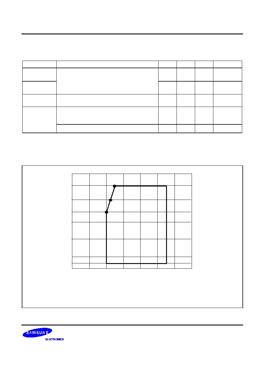
INSTRUCTION CLOCK = 1/6n x oscillator frequency (n = 1, 2, 8, 16)
A 2.0 V: 4 MHz,
B 2.2 V: 6 MHz,
C 2.4 V: 8 MHz
SUPPLY VOLTAGE (V)
250 kHz
500 kHz
670 kHz
1.00 MHz
8.32 kHz
INSTRUCTION
CLOCK
1
2
3
4
5
6
7
FOSC
(Main oscillation
frequency)
6 MHz
4 MHz
400 kHz
8 MHz
1.33 MHz
A
B
C
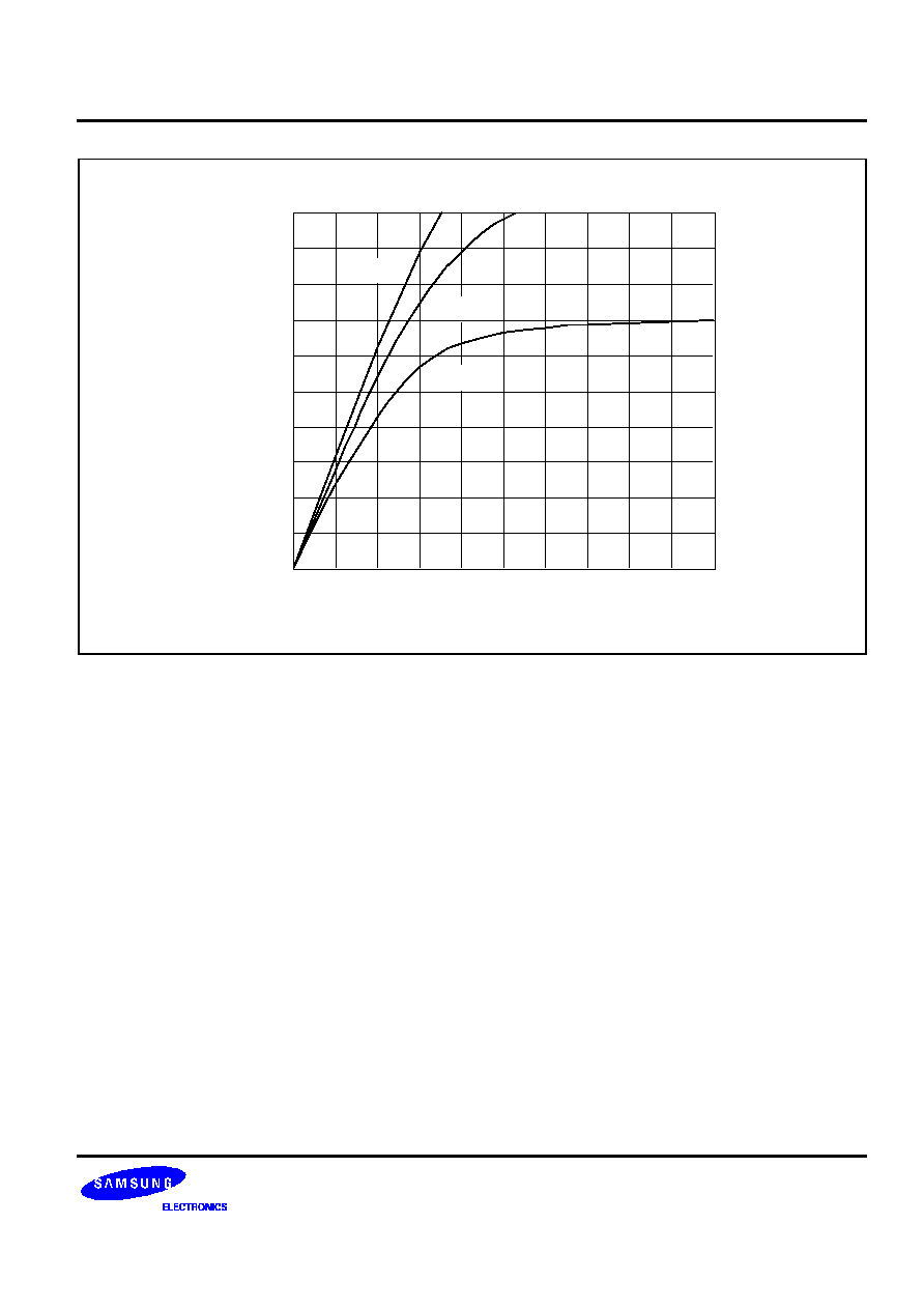
Figure 14-5. Operating Voltage Range
ELECTRICAL DATA
S3C8095/P8095
14-8
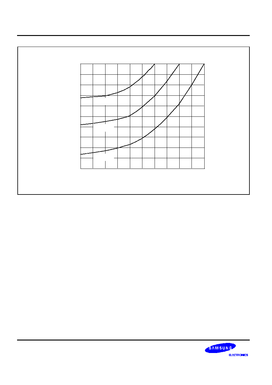
IOH
(mA)
-9
-10
VOH (V)
-8
-7
-6
-5
-4
1
1.5
2
2.5
3
3.5
4
0.5
-3
0
4.5
5
VDD = 4V
VDD = 3V
VDD = 5V
-2
0
-1
Figure 14-6. I
OH
vs. V
OH
(Port 0)
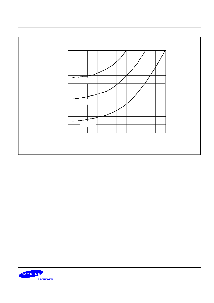
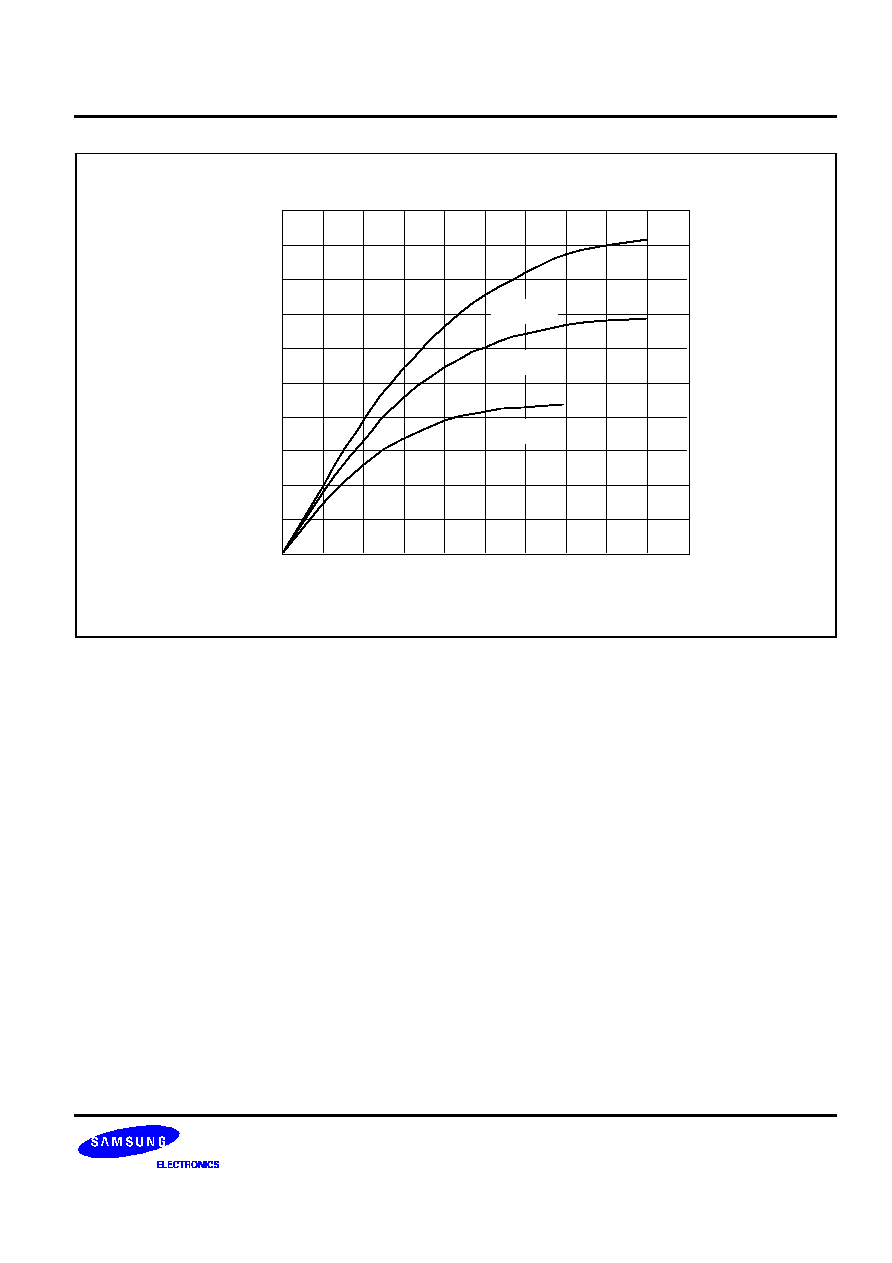
S3C8095/P8095
ELECTRICAL DATA
14-9
IOH
(mA)
-9
-10
VOH (V)
-8
-7
-6
-5
-4
1
1.5
2
2.5
3
3.5
4
0.5
-3
0
4.5
5
VDD = 4V
VDD = 3V
-2
0
-1
VDD = 5V
Figure 14-7. I
OH
vs. V
OH
(Port 2)
ELECTRICAL DATA
S3C8095/P8095
14-10
IOH
(mA)
-36
-40
VOH (V)
-32
-28
-24
-20
-16
1
1.5
2
2.5
3
3.5
4
0.5
-12
0
4.5
5
VDD = 4V
VDD = 3V
-8
0
-4
VDD = 5V
Figure 14-8. I
OH
vs. V
OH
(Port 3)
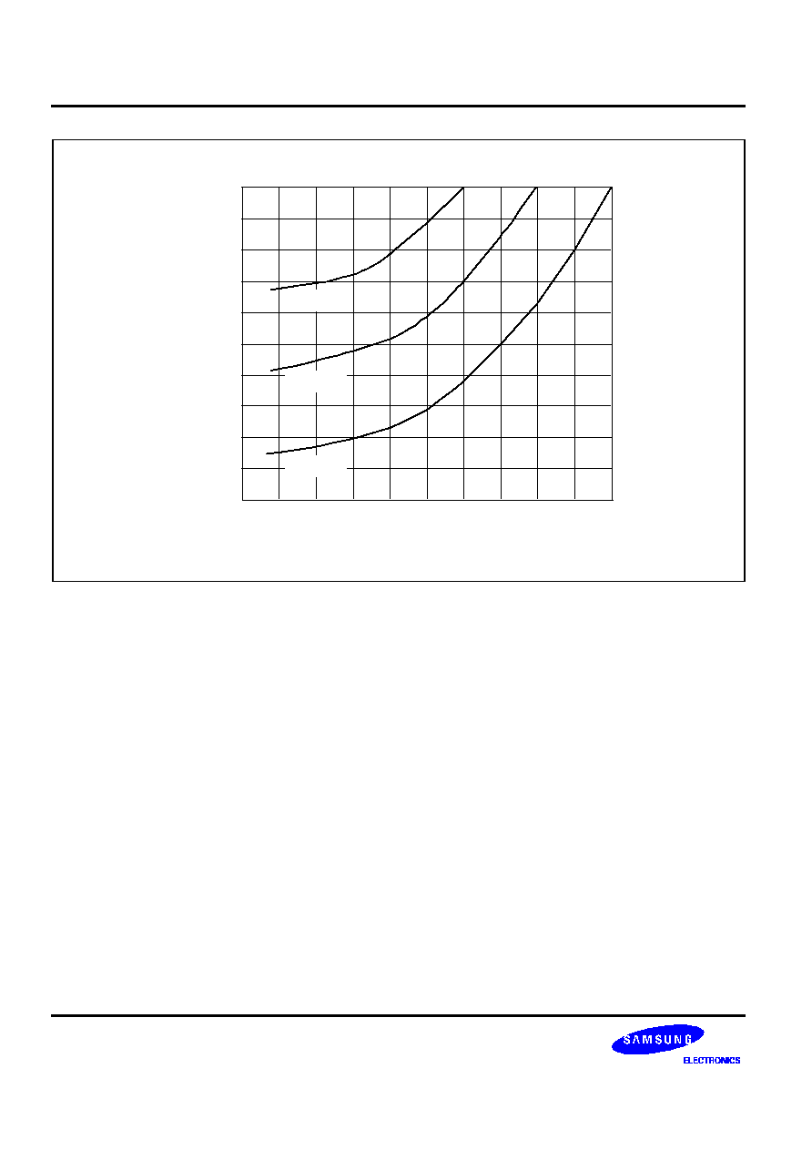
S3C8095/P8095
ELECTRICAL DATA
14-11
IOL
(mA)
2
VOL (V)
4
6
8
10
12
0.6
0.9
1.2
1.5
1.8
2.1
2.4
0.3
14
0
2.7
3
VDD = 4V
VDD = 3V
16
20
18
VDD = 5V
Figure 14-9. I
OL
vs. V
OL
(Port 0)
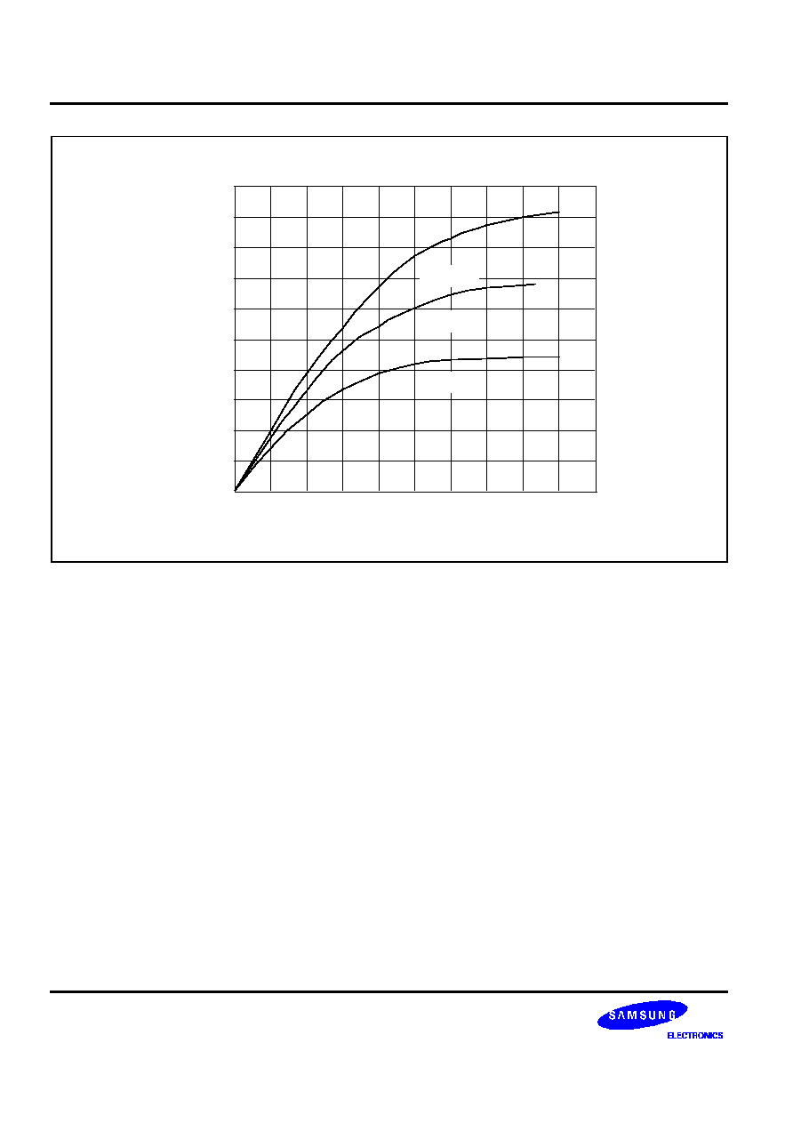
ELECTRICAL DATA
S3C8095/P8095
14-12
IOL
(mA)
2
VOL (V)
4
6
8
10
12
0.6
0.9
1.2
1.5
1.8
2.1
2.4
0.3
14
0
2.7
3
VDD = 4V
VDD = 3V
16
20
18
VDD = 5V
Figure 14-10. I
OL
vs. V
OL
(Port 2)
S3C8095/P8095
ELECTRICAL DATA
14-13
IOL
(mA)
5
VOL (V)
15
20
25
30
35
0.7
1.05
1.4
1.75
2.1
2.45
2.8
0.35
40
0
3.15
3.5
VDD = 4V
VDD = 3V
45
10
50
VDD = 5V
Figure 14-11. I
OL
vs. V
OL
(Port 3)
S3C8095/P8095
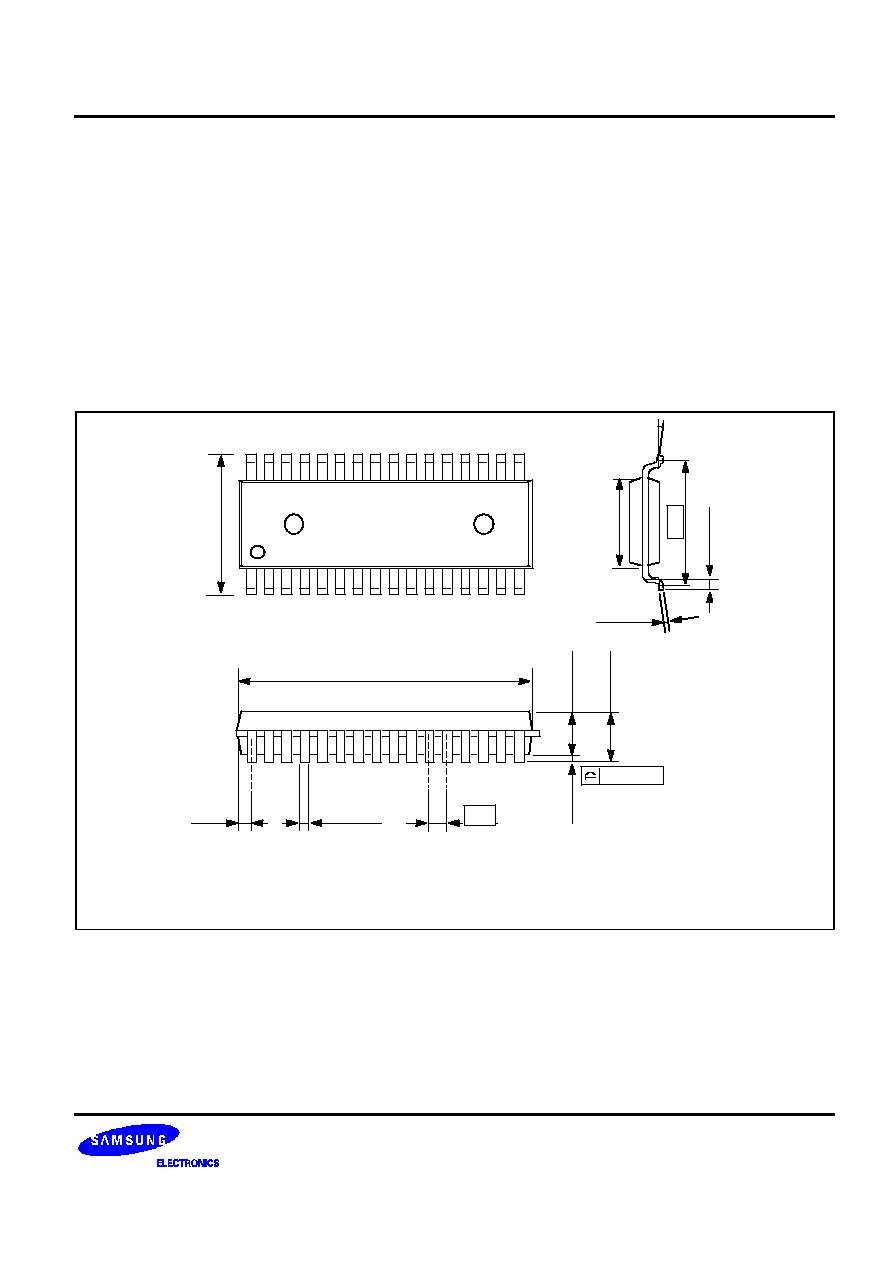
MECHANICAL DATA
15-1
15
MECHANICAL DATA
OVERVIEW
The S3C8095 microcontroller is currently available in a 32-pin SOP package.
0~8∞
0.20
+0.10
- 0.05
8.34
± 0.2
0.78
± 0.20
11.43
#1
#16
#32
#17
32-SOP-450A
12.00
± 0.3
NOTE: Dimensions are in millimeters.
19.90
± 0.2
0.10 MAX
0.0MIN
2.00
± 0.2
2.40MAX
(0.43)
0.40
± 0.1
1.27
Figure 15-1. 32-Pin SOP Package Mechanical Data
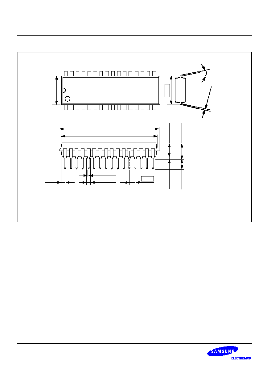
MECHANICAL DATA
S3C8095/P8095
15-2
NOTE: Dimensions are in millimeters.
32-SDIP-400
9.10 ± 0.20
#1
#16
#32
#17
0 ≠ 15
∞
0.25
+0.1 ≠ 0.05
10.16
0.51MIN
3.80
± 0.2
3.30
± 0.3
5.08MAX
(1.37)
27.48
± 0.2
27.88 MAX
1.778
0.45 ± 0.10
1.00 ± 0.10
Figure 15-2. 32-Pin SDIP Package Mechanical Data