 | ÐлекÑÑоннÑй компоненÑ: KS1453 | СкаÑаÑÑ:  PDF PDF  ZIP ZIP |
KS1453_F.PDF

KS1453
DATA PROCESSOR
1
INTRODUCTION
The KS1453 is a Data Process IC which acts as a buffer control for outputting the demodulated data by Hand
Shake. It also executes error corrections of the Sliced output of the RF signal from the disc (EFM signals). It is
compatible with a 1
×
DVDP/DVD-ROM and a 4
×
(CLV standard) CD Data Processing. Its other functions include
ECC Error Correction, CD/DVD repeat playback, Descramble, EDC Error Detection, DSI Data Detection, A/V
Decoder Interface, CD/VCD Playback, BCA Decoding, Disc Motor Control, EFM Demodulation and
Synchronization Detection, Protection, Insertion and ID Data Error Correction.
FEATURES
· External PLCK input
· EFM/EFM Plus Demodulator
· Sync Protection/Insertion
· CIRC/RS-PC Error Correction (4/16 Erasure Correction)
· Cross/Row Deinterleave
· 4~16 Mbits DRAM Interface (External component for Error Correction/Track Buffer)
· Descramble
· ID Error Correction
· Main Data Error Detection (EDC)
· Error Flag Monitoring
· MICOM Interface
· Micom Direct Memory Access Function (DVD/CD)
· DSI Detection and DSI Data Output
· A/V Decoder Parallel Interface
· Built-in CD-DA Decoder
· Subcode Data Serial Output
· Spindle Servo Control Signal Generation
· DVD Playback
· CD/VCD Playback (1
×
, 2
×
4
×
)
· BCA Decoding function
· CLV/CAV function
· CD/VCD Repeat Correction Function
· 5 V Single Power Supply
· 128-QFP
· Application Mode: CD_Player, CD_ROM, Video-CD, DVDP Player
KS1453
DATA PROCESSOR
2
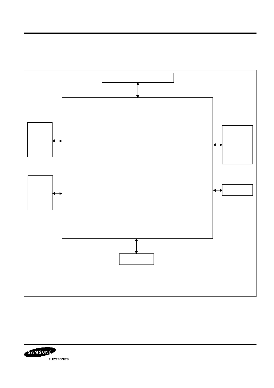
BLOCK DIAGRAM
DVD CL V/CAV
1 6 -8
DEMO D
3 2 BIT S R
X -tal & Tim ing
G e ne ra tor
Fra me Sync
DE T/PROT/INS
(1 7.57KHz)
VCO Tim ing
Ge ne rator
MICOM I/F
(2 08,192,17)
(1 82,172,11)
ECC
Descra mble r
(6 ,4,3)
e fm wr ID ECC
EDC
1 7 .5 8KHz= 2 6 .1 6M/1 488
RFCK 1 7 .5 8/7 .3 5KHz
2 6 .1 6MHz
6 7 6.0 8Hz
T o MICOM (15)
MDAT[7 :0 ]_ BI , MRZA_ IN, ZCS_ IN, M W R_IN,
MRD_IN, ZIRQZD_OUT, ZW AI T_OUT, ZRST_IN
T o DRAM
256K*16
(32)
DD[1 5:0 ]_ BI
DADR[8 :0 ]_ OUT
ZRAS _ OUT
ZUCAS _ OUT
ZL CAS _ OUT
ZOE [ 1 :0 ]_ OUT
ZW E[ 1 :0 ]_ OUT
T o AV (13)
SDATA[ 0 ]_ OUT/
CDATA
SDATA[ 1 ]_ OUT/L RCK
SDATA[ 2 ]_ OUT/B CLK
SDATA[ 3 ]_ OUT/C2PO
SDATA[ 4 ]_ OUT/S Q DT
SDATA[ 5 ]_ OUT/W FSY
SDATA[ 6 ]_ OUT/S 0 S1
SDATA[ 7 ]_ BI /SQ CK
DATREQ _ IN
CSTROB E _ OUT
DTER_OUT
DATACK_ OUT
TOS _ OUT
Mon i tor (9)
GFS_ OUT, FRSY Z_ OUT, TX_ OUT, EFM O_ OUT,
W FCK_ OUT, RFCK_ OUT, CK1 6M_OUT, DEMPHA_ OUT
CL VL OCK_ OUT
ECSY
CD CLV/CAV
2 3BIT SR
Fra me Sync
DET/PRO T/INS
(7 .35KHz)
VCO Tim ing
G e ne ra tor
M
M
W FCK 1 7 .5 8/7 .3 5KHz
(3 2,28,5)
(2 8,24,5)
CIRC
EFM
DEMOD
SUBCO DE I/F
7 5 Hz
M
7 .3 5KHz= 4 .3 218M/5 88
DVDP,
SQ -V CD
CD- G
(6 ,4,3)
trans ID ECC
De interle ave
&
RAM Co ntro l
M
V-C D ,CD - D A
T o RF (9)
PW MO[ 7 :0 ]_ OUT, BCARZ_ IN
Pow er(34)=VDD(11)+GND(23)
T est Pin (3
)
TES T0_IN, TES T1_IN, TES T2_IN
From
Se rvo (3)
EFMI_ IN
PL CK_ IN
FG_ IN
To
S ervo (6 )
M ON_OUT
M DP_ OUT
M DS_ OUT
FSW _ OUT
PL LLOCK_
OUT
SERLOCK_
OUT
X -t a l (4)
XTI_ IN
XTO_ OUT
CK3 3MI_ IN
CK3 3MO_ OUT
KS1453
DATA PROCESSOR
3
PIN DIAGRAM
KS1453
64 SDATA4_OUT
63 SDATA3_OUT
62 SDATA2_OUT
61 SDATA1_OUT
60 SDATA0_OUT
59 DVDD
58 DATACK_OUT
57 TOS_OUT
56 DVSS
55 DVSS
54 DADR3_OUT
53 DADR4_OUT
52 DADR2_OUT
51 DADR5_OUT
50 DADR1_OUT
49 DADR6_OUT
48 DADR0_OUT
47 DVSS
46 DADR7_OUT
45 DADR8_OUT
44 ZRAS_OUT
43 ZOE0_OUT
42 DVDD
41 ZOE1_OUT
40 ZWE0_OUT
39 ZWE1_OUT
6
9
C
S
T
R
O
B
E
_
O
U
T
1
0
2
W
F
C
K
_
O
U
T
1
0
1
E
F
M
O
_
O
U
T
1
0
0
T
E
S
T
2
_
I
N
9
9
T
E
S
T
1
_
I
N
9
8
T
E
S
T
0
_
I
N
9
7
D
V
D
D
9
6
C
K
3
3
M
O
_
O
U
T
9
5
C
K
3
3
M
I
_
I
N
9
4
D
V
S
S
9
3
G
F
S
_
O
U
T
9
2
T
X
_
O
U
T
9
1
F
R
S
Y
Z
_
O
U
T
9
0
D
V
S
S
8
9
D
V
S
S
8
8
D
V
S
S
8
7
D
V
S
S
8
6
D
V
D
D
8
5
D
V
D
D
8
4
D
V
S
S
8
3
D
V
S
S
8
2
D
V
S
S
8
1
P
W
M
O
0
_
O
U
T
8
0
P
W
M
O
1
_
O
U
T
7
9
P
W
M
O
2
_
O
U
T
7
8
P
W
M
O
3
_
O
U
T
7
7
D
V
D
D
7
6
P
W
M
O
4
_
O
U
T
7
5
P
W
M
O
5
_
O
U
T
7
4
P
W
M
O
6
_
O
U
T
7
3
P
W
M
O
7
_
O
U
T
7
2
D
V
S
S
7
1
D
T
E
R
_
O
U
T
7
0
D
A
T
R
E
Q
_
I
N
6
8
D
V
S
S
6
7
S
D
A
T
A
7
_
B
I
6
6
S
D
A
T
A
6
_
O
U
T
6
5
S
D
A
T
A
5
_
O
U
T
1
D
V
S
S
2
Z
C
S
_
I
N
3
M
R
Z
A
_
I
N
4
D
V
S
S
5
M
D
A
T
7
_
B
I
6
M
D
A
T
6
_
B
I
7
M
D
A
T
5
_
B
I
8
M
D
A
T
4
_
B
I
9
M
D
A
T
3
_
B
I
1
0
M
D
A
T
2
_
B
I
1
1
M
D
A
T
1
_
B
I
1
2
M
D
A
T
0
_
B
I
1
3
D
V
D
D
1
4
X
T
I
_
I
N
1
5
X
T
O
_
O
U
T
1
6
D
V
S
S
1
7
D
D
1
5
_
B
I
1
8
D
D
0
_
B
I
1
9
D
D
1
4
_
B
I
2
0
D
D
1
_
B
I
2
1
D
V
S
S
2
2
D
D
1
3
_
B
I
2
3
D
D
2
_
B
I
2
4
D
D
1
2
_
B
I
2
5
D
D
3
_
B
I
2
6
D
V
D
D
2
7
D
D
1
1
_
B
I
2
8
D
D
4
_
B
I
2
9
D
D
1
0
_
B
I
3
0
D
D
5
_
B
I
3
1
D
V
S
S
3
2
D
D
9
_
B
I
3
3
D
D
6
_
B
I
3
4
D
D
8
_
B
I
3
5
D
D
7
_
B
I
3
6
D
V
S
S
3
7
Z
L
C
A
S
_
O
U
T
3
8
Z
U
C
A
S
_
O
U
T
103 RFCK_OUT
104 PLCK_IN
105 DVSS
109 MDP_OUT
110 MDS_OUT
111 DVSS
112 DVSS
113 MON_OUT
114 FG_IN
115 FSW_OUT
116 EFMI_IN
117 DVDD
118 DVDD
119 DVDD
120 CK16M_OUT
121 DEMPHA_OUT
122 BCARZ_IN
123 DVSS
124 ZRST_IN
125 ZWAIT_OUT
126 ZIRQZD_OUT
127 MRD_IN
128 MWR_IN
106 PLLLOCK_OUT
107 CLVLOCK_OUT
108 SERLOCK_LOCK
KS1453
DATA PROCESSOR
4
PIN DESCRIPTION
No.
Pin Name
Description
I/O
Notes
1
DVSS
Digital GND (0 V)
2
ZCS_IN
Chip Select (Active Low)
I
MICOM
3
MRZA_IN
Micom Register Select (L
REGISTER H
DATA)
I
MICOM
4
DVSS
Digital GND (0 V)
5
MDAT7_BI
MICOM Data Bus
B
MICOM
6
MDAT6_BI
MICOM Data Bus
B
MICOM
7
MDAT5_BI
MICOM Data Bus
B
MICOM
8
MDAT4_BI
MICOM Data Bus
B
MICOM
9
MDAT3_BI
MICOM Data Bus
B
MICOM
10
MDAT2_BI
MICOM Data Bus
B
MICOM
11
MDAT1_BI
MICOM Data Bus
B
MICOM
12
MDAT0_BI
MICOM Data Bus
B
MICOM
13
DVDD
Digital Power (+5V)
14
XTI_IN
System Clock Input for 26.16 MHz
I
XTAL
15
XTO_OUT
System Clock Output for 26.16 MHz
O
XTAL
16
DVSS
Digital GND (0 V)
17
DD15_BI
DRAM Data Bus
B
DRAM
18
DD0_BI
DRAM Data Bus
B
DRAM
19
DD14_BI
DRAM Data Bus
B
DRAM
20
DD1_BI
DRAM Data Bus
B
DRAM
21
DVSS
Digital GND (0 V)
22
DD13_BI
DRAM Data Bus
B
DRAM
23
DD2_BI
DRAM Data Bus
B
DRAM
24
DD12_BI
DRAM Data Bus
B
DRAM
25
DD3_BI
DRAM Data Bus
B
DRAM
26
DVDD
Digital Power (+5 V)
27
DD11_BI
Digital Data Bus
B
DRAM
28
DD4_BI
Digital Data Bus
B
DRAM
29
DD10_BI
Digital Data Bus
B
DRAM
30
DD5_BI
Digital Data Bus
B
DRAM
31
DVSS
Digital GND (0 V)
32
DD9_BI
DRAM Data Bus
B
DRAM
33
DD6_BI
DRAM Data Bus
B
DRAM
34
DD8_BI
DRAM Data Bus
B
DRAM
35
DD7_BI
DRAM Data Bus
B
DRAM
36
DVSS
Digital GND (0 V)
37
ZLCAS_OUT
DRAM Low Column Address Strobe
O
DRAM
38
ZUCAS_OUT
DRAM Upper Column Address Strobe
O
DRAM
39
ZWE1_OUT
DRAM Write Enable 1 (8M ONLY)
O
DRAM
40
ZWE0_OUT
DRAM Write Enable 0 (4M, 8M, 16M)
O
DRAM
41
ZOE1_OUT
DRAM Output Enable 1 (16M MODE DADR9)
O
DRAM
42
DVDD
Digital Power (+5 V)
43
ZOE0_OUT
DRAM Output Enable 0
O
DRAM
44
ZRAS_OUT
DRAM Row Address Strobe
O
DRAM
45
DADR8_OUT
DRAM Address Bus
O
DRAM
KS1453
DATA PROCESSOR
5
46
DADR7_OUT
DRAM Address Bus
O
DRAM
47
DVSS
Digital GND (0 V)
48
DADR0_OUT
DRAM Address Bus
O
DRAM
49
DADR6_OUT
DRAM Address Bus
O
DRAM
50
DADR1_OUT
DRAM Address Bus
O
DRAM
51
DADR5_OUT
DRAM Address Bus
O
DRAM
52
DADR2_OUT
DRAM Address Bus
O
DRAM
53
DADR4_OUT
DRAM Address Bus
O
DRAM
54
DADR3_OUT
DRAM Address Bus
O
DRAM
55
DVSS
Digital GND (0 V)
56
DVSS
Digital GND (0 V)
57
TOS_OUT
Top of Sector
O
AV Decoder
58
DATACK_OUT
Data Acknowledge Signal Output
O
AV Decoder
59
DVDD
DIGITAL Power (+5 V)
60
SDATA0_OUT
DVD Data/CD Data Bit Stream (CDATA)
O
AV Decoder
61
SDATA1_OUT
DVD Data/CD Data L/R Clock (LRCK)
O
AV Decoder
62
SDATA2_OUT
DVD Data/CD Data Bit Clock (BLCK)
O
AV Decoder
63
SDATA3_OUT
DVD Data/CD Data Error Flag (C2PO)
O
AV Decoder
64
SDATA4_OUT
DVD Data/Subcode Serial Data (SQDT)
O
AV Decoder
65
SDATA5_OUT
DVD Data/Subcode Frame Sync (WFSY)
O
AV Decoder
66
SDATA6_OUT
DVD Data/Subcode Block Sync (S0S1)
O
AV Decoder
67
SDATA7_BI
DVD Data/Subcode Serial Clock (SQCK)
B
AV Decoder
68
DVSS
Digital GND (0 V)
69
CSTROBE_OUT
Data Strobe (Clock) Output
O
AV Decoder
70
DATREQ_IN
Data Request from A/V Decoder or ROM Decoder
I
AV Decoder
71
DTER_OUT
DVD Data Error Output
O
AV Decoder
72
DVSS
Digital GND (0 V)
73
PWMO7_OUT
PWM Output Signal
O
RF
74
PWMO6_OUT
PWM Output Signal
O
RF
75
PWMO5_OUT
PWM Output Signal
O
RF
76
PWMO4_OUT
PWM Output Signal
O
RF
77
DVDD
Digital Power (+5 V)
78
PWMO3_OUT
PWM Output Signal
O
RF
79
PWMO2_OUT
PWM Output Signal
O
RF
80
PWMO1_OUT
PWM Output Signal
O
RF
81
PWMO0_OUT
PWM Output Signal
O
RF
82
DVSS
Digital GND (0 V)
83
DVSS
Digital GND (0 V)
84
DVSS
Digital GND (0 V)
85
DVDD
DIGITAL Power (+5 V)
86
DVDD
DIGITAL Power (+5 V)
87
DVSS
Digital GND (0 V)
88
DVSS
Digital GND (0 V)
89
DVSS
Digital GND (0 V)
90
DVSS
Digital GND (0 V)
91
FRSYZ_OUT
Frame Sync Out
O
Monitor
92
TX_OUT
Digital Out
O
Monitor
No.
Pin Name
Description
I/O
Notes
KS1453
DATA PROCESSOR
6
93
GFS_OUT
Good Frame Sync Detection State Output (OK at H)
O
Monitor
94
DVSS
Digital GND (0 V)
95
CK33MI_IN
System Clock Input for 33.8688 MHz
I
X-tal
96
CK33MO_OUT
System Clock Output for 33.8688 MHz
O
X-tal
97
DVDD
Digital Power (+5 V)
98
TEST0_IN
Test Mode Selection Terminal
I
99
TEST1_IN
Test Mode Selection Terminal
I
100
TEST2_IN
Test Mode Selection Terminal
I
101
EFMO_OUT
EFM Out
O
Monitor
102
WFCK_OUT
Write Frame Pulse
O
Monitor
103
RFCK_OUT
Reference Frame Pulse
O
Monitor
104
PLCK_IN
Phase Locked Clock
I
Servo
105
DVSS
Digital GND (0 V)
106
PLLLOCK_OUT
Lock Signal for PLL
O
Servo
107
CLVLOCK_OUT
Lock Signal for CLV
O
Monitor
108
SERLOCK_OUT
Lock Signal for SERVO
O
Servo
109
MDP_OUT
Spindle Motor Phase Control Signal (3-STATE)
O
Servo
110
MDS_OUT
Spindle Motor Speed Control Signal (3-STATE)
O
Servo
111
DVSS
Digital GND (0 V)
112
DVSS
Digital GND (0 V)
113
MON_OUT
Spindle Motor Output Filter Switching Output
O
Servo
114
FG_IN
Reference Signal for CAV
I
Servo
115
FSW_OUT
Spindle Motor Output Filter Switching Output (3-STATE)
O
Servo
116
EFMI_IN
EFM/EFM+ Signal Input
I
Servo
117
DVDD
Digital Power (+5 V)
118
DVDD
Digital Power (+5 V)
119
DVDD
Digital Power (+5 V)
120
CK16M_OUT
CK33M's 2 Division Clock / 16.9344 MHz
O
Monitor
121
DEMPHA_OUT
"HIGH", when on Deemphasis
O
Monitor
122
BCARZ_IN
BCA Input Signal
I
RF
123
DVSS
Digital GND (0 V)
124
ZRST_IN
Hardware Reset (Active Low)
I
MICOM
125
ZWAIT_OUT
Micom Read / Write Access Wait (Wait at L)
O
MICOM
126
ZIRQZD_OUT
Interrupt Request to Micom
O
MICOM
127
MRD_IN
Micom Read Strobe (Active Low)
I
MICOM
128
MWR_IN
Micom Write Strobe (Active Low)
I
MICOM
No.
Pin Name
Description
I/O
Notes
KS1453
DATA PROCESSOR
7
ELECTRICAL CHARACTERISTICS
DC CHARACTERISTICS
(VDD = 5.0 V + 5%, VSS = 0 V, Ta = 0 ~ +70
°
C)
NOTES:
: All CMOS input terminal, BIDIR PAD's input mode terminal
: All Output Signals
: All CMOS input terminal, BIDIR PAD's input mode terminal
: All inputs having Pull-down
: All inputs having Pull-up
Item
Conditions
Min
Max
Unit
Applicable
Terminal
Input
Voltage
Input Voltage
"H" Level
V
IH
0.7 V
DD
V
Input Voltage
"L" Level
V
IL
0.3 V
DD
V
Output
Voltage
Output Voltage
"H" Level
V
OH
I
OH
= -2, -4 mA
2.4
V
DD
V
Output Voltage
"L" Level
V
OL
I
OL
= 2, 4 mA
0
0.4
V
Input
Current
Input Current
"H" Level
I
IH1
V
IN
= V
DD
-10
+10
µ
A
Input Current
"L" Level
I
IL1
V
IN
= V
SS
-10
+10
µ
A
Input
Current
Input Current
"H" Level
I
IH2
V
IN
= V
DD
10
100
µ
A
Input Current
"L" Level
I
IL2
V
IN
= V
SS
-100
-10
µ
A
Input LEAK Current
I
LI
V
I
= 0 ~ 5. 25 V
-10
+10
µ
A
KS1453
DATA PROCESSOR
8
ABSOLUTE MAXIMUM RATINGS
RECOMMENDED OPERATION CONDITIONS
No.
Item
Symbol
Spec.
Unit
1
DC input voltage
Vin
-0.3 ~ VDD + 0.3
V
2
DC supply voltage
V
DD
max
-0.3 to +7.0
V
3
DC input current
lin
+10
mA
4
Storage Temperature
Tstg
-40 ~ 125
°
C
No.
Item
Symbol
Spec.
Unit
1
Operating Temperatures
Topr
0 ~ 70
°
C
2
DC supplied voltage
V
DD
4.75 ~ 5.25
V

KS1453
DATA PROCESSOR
9
BLOCK CHARACTERISTICS
ECC FEATURE
- Uses Euclid's Algorithm
- Uses the same circuit as DVD, BCA, and CD
1) In the case of DVD (primitive polynomial: )
:Error Correcting Capability for DVD Data.
PI (182, 172, 11) CODE: 5 error correction/10 errata correction
PO (208, 192, 17) CODE: 8 error correction/16 errata correction
:Error Correction Capability for BCA Data.
BCA (52, 48, 5) CODE: 2 error correction
- 33.8688 MHz Clock: 1X
operation (PI + PO + PI)/1 EFM BLOCK Satisfaction - Basic Operation.
2) In the case of CD (primitive polynomial:
)
C1 (32, 28, 5) CODE: 2 errata corrected
C2 (28, 24, 4) CODE: 4 errata corrected
- In the case of video - CD, repeat correction is executed (C1
C2
C1
C2)
MEMORY CONTROL FEATURE
- The CD Data Processor and DVD Data Processor share an external 4M or 8M DRAM.
- Has EFM Data Write, ECC Data R/W, Descrambler R/W and Transfer Read Addressing features.
- Over/Under Memory Control (VBR Control)
1) In the case of DVD
- User a 33.8688MHz Crystal Clock
- Continual storage by input order, unrelated to Data type (PO Deinterleave)
- 13 ECC Block Areas in the 4MBit DRAM (Performs EFM, ECC, Descrambler, Transfer)
- BCA Area secured (208 Bytes)
- Micom User Area secured (can use Blocks 1 ~ 8 in units of ECC Blocks)
- Can Write in units of Sectors in EFM Data Write
- Can transmit in units of Sectors when transmitting Data
- Block Copy Feature (can specify number of Sectors)
- MICOM Direct Access on DRAM
x
8
x
4
x
3
x
2
1
+
+
+
+
x
8
x
4
x
3
x
2
1
+
+
+
+
KS1453
DATA PROCESSOR
10
Figure 1. Block Diagram Of Memory Controller
2) In the case of CD
- CD-DA, CD-ROM, V-CD: Uses 33.8688MHz Crystal Clock
- VIDEO-CD: Repeat Correction Possible
- Uses 8 Kilobytes Memory Area
- EFM, ECC, Transfer function
- EFM: WFCK Standard
- ECC, Transfer: RFCK Standard
- Micom Direct Access on DRAM
3) Descrambler & EDC & Transfer Feature
- Control of Descramble On/Off from Micom
- ECD Flag output to Micom
- Choice between 2048 Bytes or 2064 Bytes for output
- Adjustable transmission sector number
- Maximum transmission rate 5.4 Mbyte/s
- Parallel synchronous I/F application
- Active "L/H" selection possible for REQUEST, TOS, ACK, DATCLK, and EDCFLG
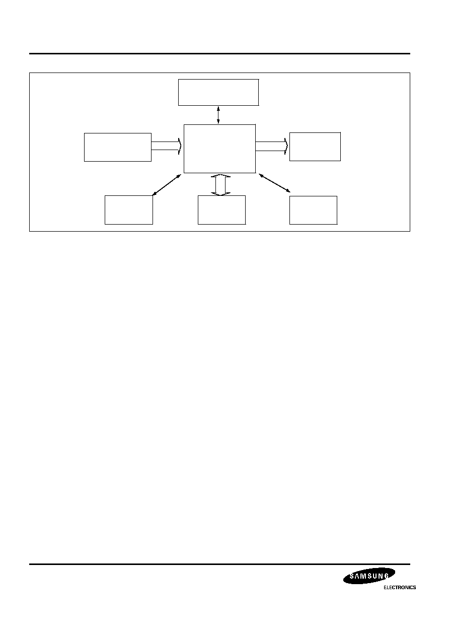
DRAM Control
-ECCMEM
-DVDMEM
-CDMEM
Dscramble
& EDC
Transfer
ECC
MICOM
External 4 M Bit
DRAM
EFM + Modulator
KS1453
DATA PROCESSOR
11
Figure 2. Transmitter Block Diagram
4) CD Audio Feature
- Data with all its errors corrected is input in Bytes, and output serially
- In case of CD - DA, Interpolation, Mute and Attenuation are handled.
5) Subcode I/f Feature
- Serially outputs the Subcode Data (P, Q, R, S, T, V, W) for CD Graphic handling
- Outputs the Subcode Data (Q) for Disc Control after checking for Errors
(
)
6) BCA Feature
- BCA Code Structure
. 4 RS ECC code max (52, 48) codes/Number of Pure information Bytes - 188 Bytes
. Composed of maximm 208 Bytes. Interleaved in units of 4 Bytes.
. Disc Rotation Speed: 1440 rpm (24 Hz), Channel bit time width - 8.89 us (01 or 10)
- BCA Block Implementation
. Data PLL is designed as an X-tal based clock
. 188 * 8 bits information bits EDC check (32 bits )
. PE RZ mod. [0]
10, [1]
01
. BCK Data and Size Detection
. Sync detection (Sync byte, Resync) and Demodulation
. Memory control design for deinterleave and buffering, ECC and EDC
. ECC decoding for 4 (52, 48) codes
DRAM
DESCRAMBLER
DRAM DATA
EDC & Built in
EDCFLG
Transmission
DRAM Cantrol
Signal
Address Generater
DATA
Transmission
MICOM I/F
MICOM
Setting Valul
Descramble DATA
Transmission
Enable Signal
REQ, TOS, ACK, DATCLK
With CSS
p x
( )
x
16
x
12
x
5
1
+
+
+
=
x
32
x
31
x
4
1
+
+
+
KS1453
DATA PROCESSOR
12
7) EFM Demodulator Feature
- CD Player, CD - ROM, DVD Player Mode Operation
- Demodulator: EFM + Demodulation (DVD)
EFM Demodulation (CD)
- ID Sync, Frame Sync Detection/Protection/Insertion:
4 step ID Sync/Frame Sync Protection Window section selection
4 step ID Sync/Frame Sync Insertion Frame Number selection
- SID Error Correction
- ID (Frame) Sync Continuous Check
8) Micom I/F Feature
- Address/Command Data: 1 Byte
- Read/Write Register Access
9) DSI I/F Feature
In the 2048 Main Data of the DVD Decoder:
. System Header Start Code (00, 00, 01, BB) from the 15
th
Byte
. Packet Header (00, 00, 01, BF, **, **) from the 39
th
Byte, Sub_Stream_id
The sector is determined to be DSI Pack and DSINT is set to "1". When CLRINT bit is "1", and the MICOM read
in S4A4B [A8] Register Conditions, it becomes cleared to "0"
. Don't care in CD MODE
DT0
DT1
DT2
DT
14 ~
DT
~ 17
DT
~ 38
DT
~ 44
DT
45
........
DT
2047
DT0
DT1
DSI Area
2048 Main Data Within Sector 1.
KS1453
DATA PROCESSOR
13
INTERFACE
MICOM I/F
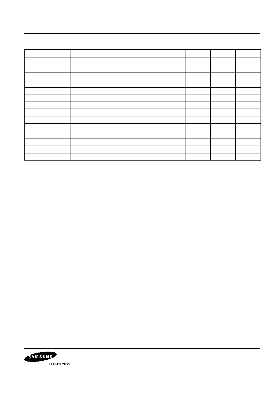
MICOM I/F Timing Diagram
Figure 3. Read Cycle
Figure 4. Write Cycle
MRZA
MWR
MRD
MDAT(7:0
)
ZCS
Data
Addr
MRZA
MWR
MRD
MDAT(7:0
)
ZCS
Data
Addr
KS1453
DATA PROCESSOR
14
Figure 5. Read Cycle
Figure 6. Write Cycle
MRZA
MWR
MRD
MDAT(7:0
)
ZCS
T
MRZA-SE TUP
T
MRZA-HOLD
T
ZCS-SE TUP
T
ZCS-HOLD
T
MWR-INA CTI VE
T
MRD-ACTI VE
T
REA D-VA LID
T
H2
T
RDAT-HOLD
T
MRD-INA CTI VE
T
H1
MRZA
MRD
MWR
MDAT(7:0
)
ZCS
T
MRZA-SE TUP
T
MRZA-HOLD
T
ZC S-SE TUP
T
ZCS-SE TUP
T
MRD-INA CTI VE
T
MWR-ACTI VE
T
MWR-INA CTI VE
VALID
T
WDAT-SE TUP
T
WDAT-HOLD
KS1453
DATA PROCESSOR
15
NOTE: There are to be no glitches in the MRZA, ZCS, MWR, and MRD signal
Time
Description
Min
Max
Unit
T
MRZA-SETUP
MRZA SETUP
0
ns
T
MRZA-HOLD
MRZA HOLD
10
ns
T
ZCS-SETUP
ZCS SETUP
10
ns
T
ZCS-HOLD
ZCS HOLD
10
ns
T
MWR-INACTIVE
MWR INACTIVE
30
ns
T
MWR-ACTIVE
MWR ACTIVE PULSE WIDTH
30
ns
T
MRD-INACTIVE
MRD INACTIVE
30
ns
T
MRD-ACTIVE
MRD ACTIVE PULSE WIDTH
120
ns
T
READ-VALID
MRD ACTIVE TO READ DATA VALID
60
ns
T
H1
MRD ACTIVE TO MDAT(7:0) LOW IMPEDANCE
-
ns
T
H2
MRD INACTIVE TO MDAT(7:0) HIGH IMPEDANCE
-
-
ns
T
RDAT-HOLD
READ DATA HOLD AFTER MRD INACTIVE
10
ns
T
WDAT-SETUP
WRITE DATA SETUP
20
ns
T
WDAT-HOLD
WRITE DATA HOLD
10
ns
KS1453
DATA PROCESSOR
16
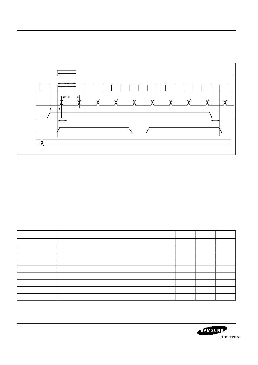
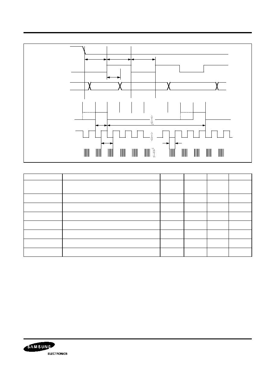
AV DECODER I/F
: Burst out Mode (DVD-P I/F (C-Qube) Synchronous, Samsung Multi, Sanyo)
MODE1: 2048 Bytes Main data only --> compared to MODE2 T
DATA-ACCESS
is delayed for about T.
MODE2: 2064 Bytes data in a Sector
(4 Bytes ID + 2 Bytes IEC + 6 Bytes RSV + 2048 Bytes Main Data + 4 Bytes EDC)
*DTER Signals are output in units of sectors
*Data must be taken from CSTROBE/DATACLK's falling Edge (In reverse mode, Rising edge).
*CSTROBE/DATACLK's duty cycle is not regular, and DATACK
*T
CSPULSE-HIGH/LOW
: 4T
*T
CSPULSE-CYCLE
: 8T (240 ns)
* CSTROBE, DATREQ, DATACK's EDGE is programmable (Reversible).
- Timing Spec
Time
Description
Min
Max
Unit
T
DATA-SETUP-STR
SDATA(7:0) Setup to CSTROBE Asserted (Synchronous)
5
ns
T
SDATA-D
SDATA(7:0) Hold from CSTROBE Asserted (Synchronous)
5
ns
T
D
Delay from DATREQ Asserted to DATACK (Asynchronous)
0
ns
T
ACK-LOW
DATACK Low Time (Asynchronous)
50
ns
T
ACK-P
DATACK Period
75
ns
T
ACK-DIS
DATACK Disabled Time
12
ns
T
SDATA-D
SDATA(7:0) Delay from DATACK Falling
10
ns
T
ACK-SETUP
DATACK Setup to CSTROBE (Synchronous)
5
ns
T
ACK-HOLD
DATACK Hold from CSTROBE (Synchronous)
5
ns
T
DATA-SET UP-ST R
T
ACK-SET UP
T
ACK-HO LD
T
CSPUL SE-HI GH
T
CSPUL SE-LO W
T
CSPUL SE-CYCL E
T
DATA-ACC ESS
T
DATA-HO LD -ST R
T
W -T OS
INV A LID
S DA TA (7 :0)
DA TRE Q
DA TA CK
DTE R
CS TRO B E /
DA TA CL K
TO S
KS1453
DATA PROCESSOR
17
CD - DA/ CD - ROM/ V-CD DATA OUTPUT TIMING
BCLK
LRCK
CDATA
Right Channel
Left Channel
C2PO(ROM,
V-CD)
C2PO(CD-DA)
L_ch Error
R_ch Error
(b)
Format 2
BCLK
LRCK
CDATA
15 14 13 12 11 10 9 8 7 6
5 4 3
2 1 0
Right Channel
Left Channel
Invalid
15 14 13 12 11 10 9 8
7 6 5
4
Invalid
C2PO(ROM,
V-CD)
for Upper Byte (H=error)
for Lower Byte (H=error)
C2PO(CD-DA)
L_ch Error
R_ch Error
(a)
Format 1
for Upper Byte (H=error)
0
1 2 3 4
5
6 7 8 9 10 11 12 13 14 15
Invalid
for Upper Byte (H=error)
for Lower Byte (H=error)
0 1 2
3 4 5 6 7 8
9 10
Invalid
for Upper Byte (H=error)
KS1453
DATA PROCESSOR
18
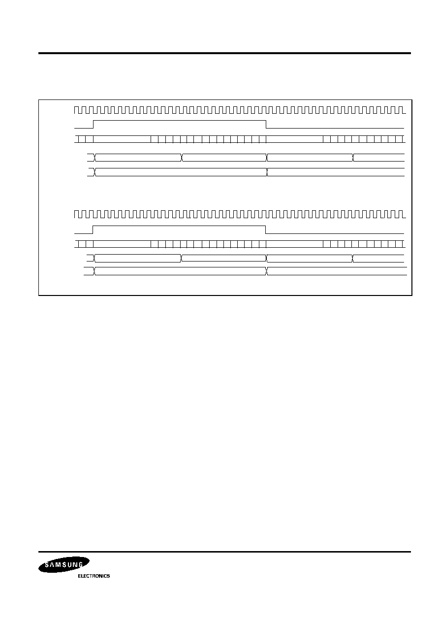
SUBCODE OUTPUT I/F (FOR CD-G)
: After WFSY becomes falling edge, SQCK becomes 'L' during about 10
µ
sec.
: If S0S1 is 'L' Subcode P is output, and if 'H' Subcode sync S0 and S1 is output.
: If pulses are input into the SQCK terminal over seven, Subcode Data (P,Q,R,S,T,U,V, W) are repeated
x
1 Subcode SYNC = 98 EFM Frames (1 EFM Frame = 7.35 KHz, 1 Subcode SYNC = 75 Hz)
x
98 EFM Frames = 2 Bytes for Subcode SYNC (S0, S1) + 96 Bytes for Subcode Data
x
96 Bytes Subcode Data = 1 (P) Bit
×
96 + 1 (Q) Bit
×
80 + 16 Bits (CRC for EDC) for CDP
+ 6 (R ~ W) Bits
×
96 for CDG
¨é
¨ç
¨è
8
7
6
5
4
3
2
1
Q
R
S
T
U
V
W
WFSY
SQCK
SQDT
S0S1
WFSY
S0S1
0
1
2
3
4
5
6
....
95
96
97
SQCK
SQDT
P
Q
R
S
T
U
V
W
KS1453
DATA PROCESSOR
19
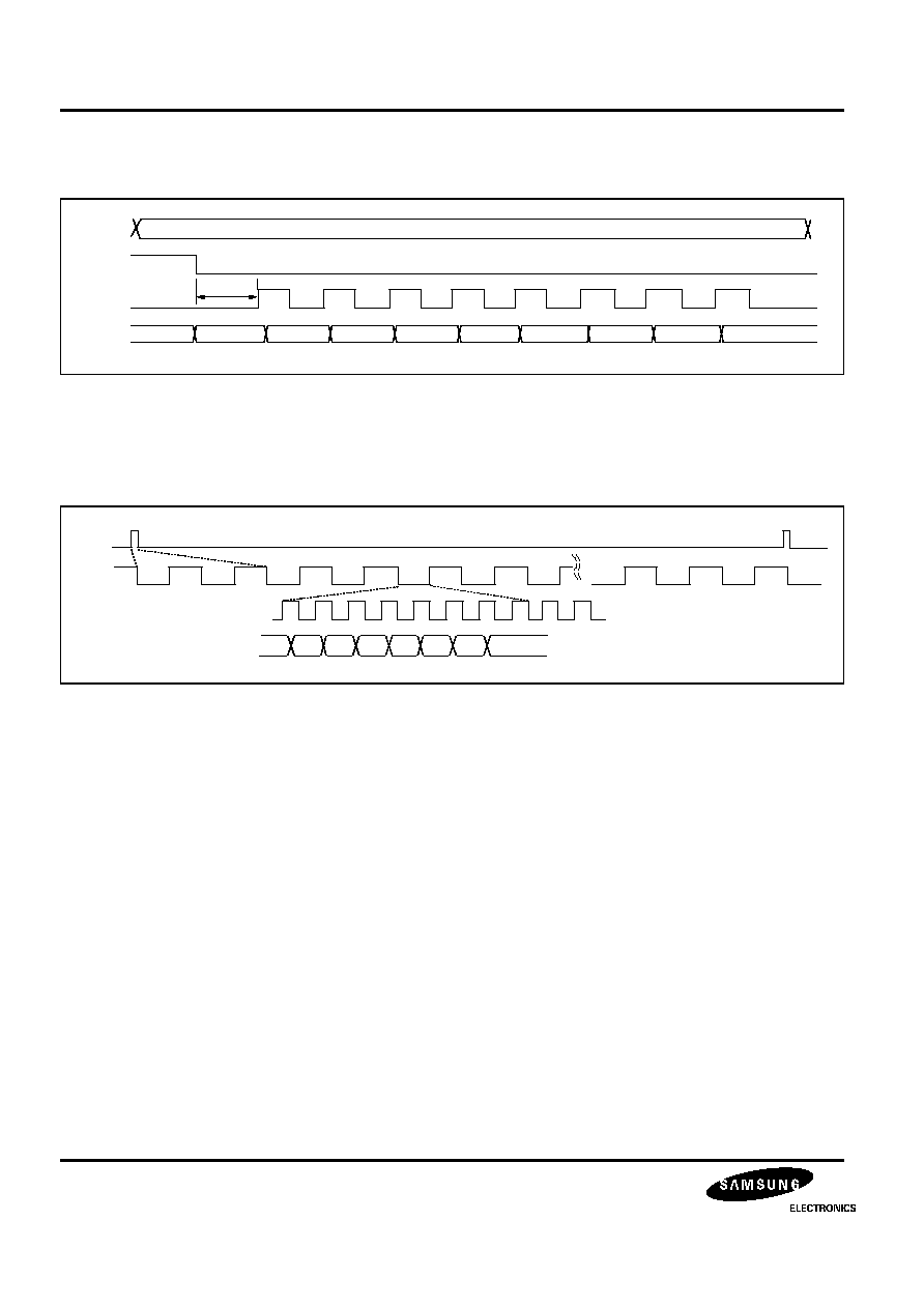
NOTE: Complete SQDT READ in the WFSY LOW Section (T
WFSYLW
).
Time
Description
Min
Typ
Max
Unit
T
D
Delay Time from WFSY LOW to SQCK HIGH
edge for "P" Subcode bit (SQCK input)
1
-
-
µ
s
T
SQCKHW
SQCK (input) HIGH Pulse Width
1
-
3
µ
s
T
SQCKLW
SQCK (input) LOW pulse Width
1
-
3
µ
s
T
HOLD
SQDT Hold Time from SQCK HIGH
0
-
-
ns
T
S0S1HW
S0S1 HIGH Pulse Width
-
136
-
µ
s
T
BP
Block Period
-
13
-
ms
T
FP
Frame Period
-
136
-
µ
s
T
WFSYLW
WFSY LOW Pulse Width
-
68
-
µ
s
WFSY
S0S1
SQCK
SQDT
T
D
T
S QCK H W
T
S QCK LW
T
H OLD
WFSY
SQCK
P
Q
R
Byte0 Byte1 Byte2 Byte3 Byte4 ..........
Byte97 Byte0 Byte1
T
S0S1HW
T
BP
T
FP
T
WFSY LW
KS1453
DATA PROCESSOR
20
EXTERNAL DRAM MEMORY MAP
Figure 7. External DRAM Memory MAP
DPDATA (208x2048 Byte)
PO (208x182 Byte)
ID+IEC+RSV+EDC(208x16 Byte)
1 1001 1111 (415)
1 1010 0000 (416)
13 ECC Block
--> 208 Sector
PI (208x120 Byte)
Un-used
1 1011 1001 (441)
1 1100 0000 (448)
1 1111 0111 (503)
1 1110 1111 (495)
1 1111 1111 (511)
1 1111 0011 (496)
1 1111 1000 (504)
0 0000 0000 (0)
KS1453
DATA PROCESSOR
21
APPLICATION CIRCUIT
KS1453
4 M Bit DRAM
MPEG
DECODER
CDG
RF
(KS1461)
SERVO
(KS1452)
P17~P20,P22~P25,P27~P30,P32~P35: DD[15:0]_OUT /
P45~P46,P48~P54: DADR[8:0]_OUT /
P39,P40: ZWE[1:0]_OUT / P41,P43: ZOE[1:0]_OUT /
P37: ZLCAS_OUT / P38: ZUCAS_OUT / P44: ZRAS_OUT
P5~P12: MDAT[7:0]_BI / P124: ZRST_IN
P2: ZCS_IN / P3: MRZA_IN
P125: ZWAIT_OUT / P126: ZIRQZD_OUT
P127: MRD_IN / P128: MWR_IN
P73~P76,P78~P81:
PWMO[7:0]_OUT
P122: BCARZ_IN
P60
~P66: SDATA[0:6]_OUT
P67: SDATA[7]_BI
P57: TOS_OUT
P58: DATACK_OUT
P69: CSTROBE_OUT
P70: DATREQ_IN
P71: DTER_OUT
P60: CDATA
P61: LRCK
P62: BLCK
P63: C2PO
P64: SQDT
P65: WFSY
P66: SOS1
P67: SQCK
P98: TEST0_IN
P99: TEST1_IN
P100:TEST2_IN
P104: PLCK_IN
P114: FG_IN
P116: EFMI_IN
P106: PLLLOCK_OUT
P107: CLVLOCK_OUT
P108: SERLOCK_OUT
P109: MDP_OUT
P110: MDS_OUT
P113: MON_OUT
P114: FSW_OUT
MICOM
DVD
Mode
CD
Mode
KS1453
DATA PROCESSOR
22
PKG INFORMATION
20.00
22.00
1
4
.
0
0
1
6
.
0
0
128-QFP
0.05 MIN
3.0 MAX
0.5
0.5
0.2
1.0
KS1453