 | –≠–ª–µ–∫—Ç—Ä–æ–Ω–Ω—ã–π –∫–æ–º–ø–æ–Ω–µ–Ω—Ç: SH7145 | –°–∫–∞—á–∞—Ç—å:  PDF PDF  ZIP ZIP |
Document Outline
- Cover
- Cautions
- General Precautions on the Handling of Products
- Configuration of this Manual
- Preface
- Contents
- Figures
- Tables
- Section 1 Overview
- Section 2 CPU
- Section 3 MCU Operating Modes
- Section 4 Clock Pulse Generator
- Section 5 Exception Processing
- Section 6 Interrupt Controller (INTC)
- Section 7 User Break Controller (UBC)
- Section 8 Data Transfer Controller (DTC)
- Section 9 Bus State Controller (BSC)
- Section 10 Direct Memory Access Controller (DMAC)
- Section 11 Multi-Function Timer Pulse Unit (MTU)
- Section 12 Watchdog Timer
- Section 13 Serial Communication Interface (SCI)
- Section 14 I2C Bus Interface (IIC) Option
- Section 15 A/D Converter
- Section 16 Compare Match Timer (CMT)
- Section 17 Pin Function Controller (PFC)
- 17.1 Register Descriptions
- 17.1.1 Port A I/O Register L, H (PAIORL, H)
- 17.1.2 Port A Control Registers L2, L1, and H (PACRL2, PACRL1, and PACRH)
- 17.1.3 Port B I/O Register (PBIOR)
- 17.1.4 Port B Control Registers 1 and 2 (PBCR1 and PBCR2)
- 17.1.5 Port C I/O Register (PCIOR)
- 17.1.6 Port C Control Register (PCCR)
- 17.1.7 Port D I/O Registers L, H (PDIORL, H)
- 17.1.8 Port D Control Registers L1, L2, H1, and H2 (PDCRL1, PDCRL2, PDCRH1, and PDCRH2)
- 17.1.9 Port E I/O Register L (PEIORL)
- 17.1.10 Port E Control Registers L1 and L2 (PECRL1 and PECRL2)
- 17.1.11 High-Current Port Control Register (PPCR)
- 17.2 Precautions for Use
- Section 18 I/O Ports
- Section 19 Flash Memory (F-ZTAT Version)
- Section 20 Mask ROM
- Section 21 RAM
- Section 22 Hitachi User Debug Interface (H-UDI)
- Section 23 Advanced User Debugger (AUD)
- Section 24 Power-Down Modes
- Section 25 List of Registers
- Section 26 Electrical Characteristics
- Appendix A Pin States
- Appendix B Pin States of Bus Related Signals
- Appendix C Product Code Lineup
- Appendix D Package Dimensions
- Main Revisions and Additions in this Edition
- Index
- Colophon

Regarding the change of names mentioned in the document, such as Hitachi
Electric and Hitachi XX, to Renesas Technology Corp.
The semiconductor operations of Mitsubishi Electric and Hitachi were transferred to Renesas
Technology Corporation on April 1st 2003. These operations include microcomputer, logic, analog
and discrete devices, and memory chips other than DRAMs (flash memory, SRAMs etc.)
Accordingly, although Hitachi, Hitachi, Ltd., Hitachi Semiconductors, and other Hitachi brand
names are mentioned in the document, these names have in fact all been changed to Renesas
Technology Corp. Thank you for your understanding. Except for our corporate trademark, logo and
corporate statement, no changes whatsoever have been made to the contents of the document, and
these changes do not constitute any alteration to the contents of the document itself.
Renesas Technology Home Page: http://www.renesas.com
Renesas Technology Corp.
Customer Support Dept.
April 1, 2003
To all our customers

Cautions
Keep safety first in your circuit designs!
1. Renesas Technology Corporation puts the maximum effort into making semiconductor products better
and more reliable, but there is always the possibility that trouble may occur with them. Trouble with
semiconductors may lead to personal injury, fire or property damage.
Remember to give due consideration to safety when making your circuit designs, with appropriate
measures such as (i) placement of substitutive, auxiliary circuits, (ii) use of nonflammable material or
(iii) prevention against any malfunction or mishap.
Notes regarding these materials
1. These materials are intended as a reference to assist our customers in the selection of the Renesas
Technology Corporation product best suited to the customer's application; they do not convey any
license under any intellectual property rights, or any other rights, belonging to Renesas Technology
Corporation or a third party.
2. Renesas Technology Corporation assumes no responsibility for any damage, or infringement of any
third-party's rights, originating in the use of any product data, diagrams, charts, programs, algorithms, or
circuit application examples contained in these materials.
3. All information contained in these materials, including product data, diagrams, charts, programs and
algorithms represents information on products at the time of publication of these materials, and are
subject to change by Renesas Technology Corporation without notice due to product improvements or
other reasons. It is therefore recommended that customers contact Renesas Technology Corporation
or an authorized Renesas Technology Corporation product distributor for the latest product information
before purchasing a product listed herein.
The information described here may contain technical inaccuracies or typographical errors.
Renesas Technology Corporation assumes no responsibility for any damage, liability, or other loss
rising from these inaccuracies or errors.
Please also pay attention to information published by Renesas Technology Corporation by various
means, including the Renesas Technology Corporation Semiconductor home page
(http://www.renesas.com).
4. When using any or all of the information contained in these materials, including product data, diagrams,
charts, programs, and algorithms, please be sure to evaluate all information as a total system before
making a final decision on the applicability of the information and products. Renesas Technology
Corporation assumes no responsibility for any damage, liability or other loss resulting from the
information contained herein.
5. Renesas Technology Corporation semiconductors are not designed or manufactured for use in a device
or system that is used under circumstances in which human life is potentially at stake. Please contact
Renesas Technology Corporation or an authorized Renesas Technology Corporation product distributor
when considering the use of a product contained herein for any specific purposes, such as apparatus or
systems for transportation, vehicular, medical, aerospace, nuclear, or undersea repeater use.
6. The prior written approval of Renesas Technology Corporation is necessary to reprint or reproduce in
whole or in part these materials.
7. If these products or technologies are subject to the Japanese export control restrictions, they must be
exported under a license from the Japanese government and cannot be imported into a country other
than the approved destination.
Any diversion or reexport contrary to the export control laws and regulations of Japan and/or the
country of destination is prohibited.
8. Please contact Renesas Technology Corporation for further details on these materials or the products
contained therein.

Hitachi SuperH
RISC engine
SH7144 Series
s
H7144,SH7144F-ZTAT
s
H7145,SH7145F-ZTAT
Hardware Manual
ADE-602-254A
Rev. 2.0
09/19/02
Hitachi, Ltd.

Rev. 2.0, 09/02, page ii of xxxviii
Cautions
1. Hitachi neither warrants nor grants licenses of any rights of Hitachi's or any third party's
patent, copyright, trademark, or other intellectual property rights for information contained in
this document. Hitachi bears no responsibility for problems that may arise with third party's
rights, including intellectual property rights, in connection with use of the information
contained in this document.
2. Products and product specifications may be subject to change without notice. Confirm that you
have received the latest product standards or specifications before final design, purchase or
use.
3. Hitachi makes every attempt to ensure that its products are of high quality and reliability.
However, contact Hitachi's sales office before using the product in an application that
demands especially high quality and reliability or where its failure or malfunction may directly
threaten human life or cause risk of bodily injury, such as aerospace, aeronautics, nuclear
power, combustion control, transportation, traffic, safety equipment or medical equipment for
life support.
4. Design your application so that the product is used within the ranges guaranteed by Hitachi
particularly for maximum rating, operating supply voltage range, heat radiation characteristics,
installation conditions and other characteristics. Hitachi bears no responsibility for failure or
damage when used beyond the guaranteed ranges. Even within the guaranteed ranges,
consider normally foreseeable failure rates or failure modes in semiconductor devices and
employ systemic measures such as fail-safes, so that the equipment incorporating Hitachi
product does not cause bodily injury, fire or other consequential damage due to operation of
the Hitachi product.
5. This product is not designed to be radiation resistant.
6. No one is permitted to reproduce or duplicate, in any form, the whole or part of this document
without written approval from Hitachi.
7. Contact Hitachi's sales office for any questions regarding this document or Hitachi
semiconductor products.

Rev. 2.0, 09/02, page iii of xxxviii
General Precautions on the Handling of Products
1. Treatment of NC Pins
Note:
Do not connect anything to the NC pins.
The NC (not connected) pins are not connected to any of the internal circuitry; they are
used as test pins or to reduce noise. If something is connected to the NC pins, the
operation of the LSI is not guaranteed.
2. Treatment of Unused Input Pins
Note:
Fix all unused input pins to high or low level.
Generally, the input pins of CMOS products are high-impedance input pins. If unused pins
are in their open states, intermediate levels are induced by noise in the vicinity, a pass-
through current flows internally, and a malfunction may occur.
3. Processing before Initialization
Note:
When power is first supplied, the product's state is undefined. The states of internal
circuits are undefined until full power is supplied throughout the chip and a low level is
input on the reset pin. During the period where the states are undefined, the register
settings and the output state of each pin are also undefined. Design your system so that it
does not malfunction because of processing while it is in this undefined state. For those
products which have a reset function, reset the LSI immediately after the power supply has
been turned on.
4. Prohibition of access to undefined or reserved addresses
Note:
Access to undefined or reserved addresses is prohibited.
The undefined or reserved addresses may be used to expand functions, or test registers
may have been be allocated to these addresses. Do not access these registers; the system's
operation is not guaranteed if they are accessed.

Rev. 2.0, 09/02, page iv of xxxviii
Configuration of This Manual
This manual comprises the following items:
1. General Precautions on Handling of Product
2. Configuration of This Manual
3. Preface
4. Contents
5. Overview
6. Description of Functional Modules
∑
CPU and System-Control Modules
∑
On-Chip Peripheral Modules
The configuration of the functional description of each module differs according to the
module. However, the generic style includes the following items:
i) Feature
ii) Input/Output Pin
iii) Register Description
iv) Operation
v) Usage Note
When designing an application system that includes this LSI, take notes into account. Each section
includes notes in relation to the descriptions given, and usage notes are given, as required, as the
final part of each section.
7. List of Registers
8. Electrical Characteristics
9. Appendix
10. Main Revisions and Additions in this Edition (only for revised versions)
The list of revisions is a summary of points that have been revised or added to earlier versions.
This does not include all of the revised contents. For details, see the actual locations in this
manual.
11. Index

Rev. 2.0, 09/02, page v of xxxviii
Preface
The SH7144 Series single-chip RISC (Reduced Instruction Set Computer) microprocessor
includes a Hitachi-original RISC CPU as its core, and the peripheral functions required to
configure a system.
Target users: This manual was written for users who will be using this LSI in the design of
application systems. Users of this manual are expected to understand the
fundamentals of electrical circuits, logical circuits, and microcomputers.
Objective:
This manual was written to explain the hardware functions and electrical
characteristics of this LSI to the above users.
Refer to the SH-1, SH-2, SH-DSP Programming Manual for a detailed description
of the instruction set.
Notes on reading this manual:
∑
Product names
The following products are covered in this manual.
Product Classifications and Abbreviations
Basic Classification
On-Chip ROM Classification
Product Code
SH7144F
Flash memory version
(ROM: 256 kbytes)
HD64F7144
SH7144 (112-pin version)
SH7144M
Mask ROM version
(ROM: 256 kbytes)
HD6437144
*
SH7145F
Flash memory version
(ROM: 256 kbytes)
HD64F7145
SH7145 (144-pin version)
SH7145M
Mask ROM version
(ROM: 256 kbytes)
HD6437145
*
Note:
*
Under development
In this manual, the product abbreviations are used to distinguish products. For example, 112-
pin products are collectively referred to as the SH7144, an abbreviation of the basic type's
classification code, while 144-pin products are collectively referred to as the SH7145. There
are two versions of each: a flash memory version and a mask ROM version. When a
description is limited to the flash memory version alone, the character F is added at the end of
the abbreviation, such as SH7144F. When a description is limited to the mask ROM version
alone, an abbreviation that is determined by adding M at the end of the abbreviation.

Rev. 2.0, 09/02, page vi of xxxviii
∑
The typical product
The HD64F7144 is taken as the typical product for the descriptions in this manual.
Accordingly, when using an HD6437144, HD64F7145, or HD6437145, simply replace the
HD64F7144 in those references where no differences between products are pointed out with
HD6437144, HD64F7145, or HD6437145. Where differences are indicated, be aware that each
specification apply to the products as indicated.
∑
In order to understand the overall functions of the chip
Read the manual according to the contents. This manual can be roughly categorized into parts
on the CPU, system control functions, peripheral functions and electrical characteristics.
∑
In order to understand the details of the CPU's functions
Read the SH-1, SH-2, SH-DSP Programming Manual.
∑
In order to understand the details of a register when the user knows its name
Read the index that is the final part of the manual to find the page number of the entry on the
register. The addresses, bit names, and initial values of the registers are summarized in section
25, List of Registers.
Rules:
Register name:
The following notation is used for cases when the same or a
similar function, e.g. serial communication, is implemented
on more than one channel:
XXX_N (XXX is the register name and N is the channel
number)
Bit order:
The MSB is on the left and the LSB is on the right.
Numerical expression: Binary is B
xxxx, Hexadecimal is H
xxxx, decimal is xxxx.
Signal expression:
Low active signals are expressed as
xxxx.
Related Manuals:
The latest versions of all related manuals are available from our web site.
Please ensure you have the latest versions of all documents you require.
http://www.hitachisemiconductor.com
SH7144 Series manuals:
Manual Title
ADE No.
SH7144 Series Hardware Manual
This manual
SH-1, SH-2, SH-DSP Programming Manual
ADE-602-063

Rev. 2.0, 09/02, page vii of xxxviii
Users manuals for development tools:
Manual Title
ADE No.
C/C++ Compiler, Assembler, Optimized Linkage Editor Users Manual
ADE-702-246
Simulator Debugger (for Windows) Users Manual
ADE-702-186
Simulator Debugger (for UNIX) Users Manual
ADE-702-203
Hitachi Embedded Workshop Users Manual
ADE-702-201
Application Notes:
Manual Title
ADE No.
C/C++ Compiler Edition
ADE-702-179
F-ZTAT Technical Q & A
ADE-502-046

Rev. 2.0, 09/02, page viii of xxxviii

Rev. 2.0, 09/02, page ix of xxxviii
Contents
Section 1 Overview........................................................................................... 1
1.1
Features ............................................................................................................................. 1
1.2
Internal Block Diagram..................................................................................................... 3
1.3
Pin Arrangement ............................................................................................................... 5
1.4
Pin Functions .................................................................................................................... 7
Section 2 CPU................................................................................................... 13
2.1
Features ............................................................................................................................. 13
2.2
Register Configuration ...................................................................................................... 13
2.2.1
General Registers (Rn)......................................................................................... 13
2.2.2
Control Registers ................................................................................................. 15
2.2.3
System Registers .................................................................................................. 16
2.2.4
Initial Values of Registers.................................................................................... 17
2.3
Data Formats ..................................................................................................................... 17
2.3.1
Data Format in Registers...................................................................................... 17
2.3.2
Data Formats in Memory ..................................................................................... 17
2.3.3
Immediate Data Format ....................................................................................... 18
2.4
Instruction Features........................................................................................................... 18
2.4.1
RISC-Type Instruction Set................................................................................... 18
2.4.2
Addressing Modes ............................................................................................... 22
2.4.3
Instruction Format................................................................................................ 25
2.5
Instruction Set ................................................................................................................... 28
2.5.1
Instruction Set by Classification .......................................................................... 28
2.6
Processing States............................................................................................................... 41
2.6.1
State Transitions................................................................................................... 41
Section 3 MCU Operating Modes..................................................................... 43
3.1
Selection of Operating Modes........................................................................................... 43
3.2
Input/Output Pin................................................................................................................ 44
3.3
Explanation of Operating Modes ...................................................................................... 45
3.3.1
Mode 0 (MCU extension mode 0) ....................................................................... 45
3.3.2
Mode 1 (MCU extension mode 1) ....................................................................... 45
3.3.3
Mode 2 (MCU extension mode 2) ....................................................................... 45
3.3.4
Mode 3 (Single chip mode).................................................................................. 45
3.3.5
Clock mode .......................................................................................................... 45
3.4
Address Map ..................................................................................................................... 46
3.5
Initial State in This LSI ..................................................................................................... 46

Rev. 2.0, 09/02, page x of xxxviii
Section 4 Clock Pulse Generator ....................................................................... 47
4.1
Oscillator........................................................................................................................... 48
4.1.1
Connecting a Crystal Oscillator ........................................................................... 48
4.1.2
External Clock Input Method............................................................................... 49
4.2
Function for Detecting the Oscillator Halt........................................................................ 50
4.3
Usage Notes ...................................................................................................................... 50
4.3.1
Note on Crystal Resonator ................................................................................... 50
4.3.2
Notes on Board Design ........................................................................................ 51
Section 5 Exception Processing......................................................................... 53
5.1
Overview........................................................................................................................... 53
5.1.1
Types of Exception Processing and Priority ........................................................ 53
5.1.2
Exception Processing Operations......................................................................... 54
5.1.3
Exception Processing Vector Table ..................................................................... 55
5.2
Resets ................................................................................................................................ 57
5.2.1
Types of Reset ..................................................................................................... 57
5.2.2
Power-On Reset ................................................................................................... 57
5.2.3
Manual Reset ....................................................................................................... 58
5.3
Address Errors .................................................................................................................. 59
5.3.1
The Cause of Address Error Exception................................................................ 59
5.3.2
Address Error Exception Processing.................................................................... 60
5.4
Interrupts ........................................................................................................................... 60
5.4.1
Interrupt Sources.................................................................................................. 60
5.4.2
Interrupt Priority Level ........................................................................................ 61
5.4.3
Interrupt Exception Processing ............................................................................ 61
5.5
Exceptions Triggered by Instructions ............................................................................... 62
5.5.1
Types of Exceptions Triggered by Instructions ................................................... 62
5.5.2
Trap Instructions .................................................................................................. 62
5.5.3
Illegal Slot Instructions ........................................................................................ 63
5.5.4
General Illegal Instructions.................................................................................. 63
5.6
Cases when Exception Sources Are Not Accepted ........................................................... 63
5.6.1
Immediately after a Delayed Branch Instruction ................................................. 64
5.6.2
Immediately after an Interrupt-Disabled Instruction............................................ 64
5.7
Stack Status after Exception Processing Ends .................................................................. 65
5.8
Usage Notes ...................................................................................................................... 66
5.8.1
Value of Stack Pointer (SP) ................................................................................. 66
5.8.2
Value of Vector Base Register (VBR) ................................................................. 66
5.8.3
Address Errors Caused by Stacking of Address Error Exception Processing ...... 66
Section 6 Interrupt Controller (INTC)............................................................... 67
6.1
Features ............................................................................................................................. 67
6.2
Input/Output Pins .............................................................................................................. 69
6.3
Register Descriptions ........................................................................................................ 69

Rev. 2.0, 09/02, page xi of xxxviii
6.3.1
Interrupt Control Register 1 (ICR1)..................................................................... 70
6.3.2
Interrupt Control Register 2 (ICR2)..................................................................... 72
6.3.3
IRQ Status Register (ISR).................................................................................... 74
6.3.4
Interrupt Priority Registers A to J (IPRA to IPRJ)............................................... 75
6.4
Interrupt Sources ............................................................................................................... 77
6.4.1
External Interrupts ............................................................................................... 77
6.4.2
On-Chip Peripheral Module Interrupts ................................................................ 78
6.4.3
User Break Interrupt ............................................................................................ 78
6.4.4
H-UDI Interrupt ................................................................................................... 78
6.5
Interrupt Exception Processing Vectors Table.................................................................. 79
6.6
Interrupt Operation............................................................................................................ 82
6.6.1
Interrupt Sequence ............................................................................................... 82
6.6.2
Stack after Interrupt Exception Processing .......................................................... 84
6.7
Interrupt Response Time ................................................................................................... 85
6.8
Data Transfer with Interrupt Request Signals ................................................................... 87
6.8.1
Handling Interrupt Request Signals as Sources for DTC Activating
and CPU Interrupt, but Not DMAC Activating.................................................... 88
6.8.2
Handling Interrupt Request Signals as Sources for Activating DMAC,
but Not CPU Interrupt and DTC Activating ........................................................ 88
6.8.3
Handling Interrupt Request Signals as Source for DTC Activating,
but Not CPU Interrupt and DMAC Activating..................................................... 88
6.8.4
Handling Interrupt Request Signals as Source for CPU Interrupt
but Not DMAC and DTC Activating ................................................................... 89
Section 7 User Break Controller (UBC) ........................................................... 91
7.1
Overview........................................................................................................................... 91
7.2
Register Descriptions ........................................................................................................ 93
7.2.1
User Break Address Register (UBAR)................................................................. 93
7.2.2
User Break Address Mask Register (UBAMR) ................................................... 93
7.2.3
User Break Bus Cycle Register (UBBR) ............................................................. 94
7.2.4
User Break Control Register (UBCR).................................................................. 95
7.3
Operation........................................................................................................................... 96
7.3.1
Flow of the User Break Operation ....................................................................... 96
7.3.2
Break on On-Chip Memory Instruction Fetch Cycle ........................................... 98
7.3.3
Program Counter (PC) Values Saved................................................................... 98
7.4
Examples of Use ............................................................................................................... 99
7.5
Usage Notes ...................................................................................................................... 101
7.5.1
Simultaneous Fetching of Two Instructions......................................................... 101
7.5.2
Instruction Fetches at Branches ........................................................................... 101
7.5.3
Contention between User Break and Exception Processing ................................ 102
7.5.4
Break at Non-Delay Branch Instruction Jump Destination.................................. 102
7.5.5
Module Standby Mode Setting ............................................................................ 102

Rev. 2.0, 09/02, page xii of xxxviii
Section 8 Data Transfer Controller (DTC) ........................................................ 103
8.1
Features ............................................................................................................................. 103
8.2
Register Descriptions ........................................................................................................ 105
8.2.1
DTC Mode Register (DTMR).............................................................................. 106
8.2.2
DTC Source Address Register (DTSAR) ............................................................ 108
8.2.3
DTC Destination Address Register (DTDAR)..................................................... 108
8.2.4
DTC Initial Address Register (DTIAR) ............................................................... 108
8.2.5
DTC Transfer Count Register A (DTCRA) ......................................................... 108
8.2.6
DTC Transfer Count Register B (DTCRB) ......................................................... 109
8.2.7
DTC Enable Registers (DTER)............................................................................ 109
8.2.8
DTC Control/Status Register (DTCSR)............................................................... 110
8.2.9
DTC Information Base Register (DTBR) ............................................................ 111
8.3
Operation .......................................................................................................................... 111
8.3.1
Activation Sources ............................................................................................... 111
8.3.2
Location of Register Information and DTC Vector Table ................................... 112
8.3.3
DTC Operation .................................................................................................... 115
8.3.4
Interrupt Source ................................................................................................... 120
8.3.5
Operation Timing................................................................................................. 121
8.3.6
DTC Execution State Counts ............................................................................... 121
8.4
Procedures for Using DTC................................................................................................ 122
8.4.1
Activation by Interrupt......................................................................................... 122
8.4.2
Activation by Software ........................................................................................ 123
8.4.3
DTC Use Example ............................................................................................... 123
8.5
Cautions on Use ................................................................................................................ 124
8.5.1
Prohibition against DMAC/DTC Register Access by DTC ................................. 124
8.5.2
Module Standby Mode Setting ............................................................................ 124
8.5.3
On-Chip RAM ..................................................................................................... 124
Section 9 Bus State Controller (BSC) ............................................................... 125
9.1
Features ............................................................................................................................. 125
9.2
Pin Configuration.............................................................................................................. 127
9.3
Register Descriptions ........................................................................................................ 127
9.4
Address Map ..................................................................................................................... 128
9.5
Description of Registers.................................................................................................... 130
9.5.1
Bus Control Register 1 (BCR1) ........................................................................... 130
9.5.2
Bus Control Register 2 (BCR2) ........................................................................... 132
9.5.3
Wait Control Register 1 (WCR1)......................................................................... 136
9.5.4
Wait Control Register 2 (WCR2)......................................................................... 137
9.5.5
RAM Emulation Register (RAMER)................................................................... 137
9.6
Accessing External Space ................................................................................................. 138
9.6.1
Basic Timing........................................................................................................ 138
9.6.2
Wait State Control ............................................................................................... 139
9.6.3
CS Assert Period Extension.................................................................................141

Rev. 2.0, 09/02, page xiii of xxxviii
9.7
Waits between Access Cycles ........................................................................................... 142
9.7.1
Prevention of Data Bus Conflicts......................................................................... 142
9.7.2
Simplification of Bus Cycle Start Detection ........................................................ 143
9.8
Bus Arbitration.................................................................................................................. 144
9.9
Memory Connection Example .......................................................................................... 145
9.10
Access to On-chip Peripheral I/O Registers...................................................................... 148
9.11
Cycles of No-Bus Mastership Release .............................................................................. 148
9.12
CPU Operation When Program Is Located in External Memory ...................................... 148
Section 10 Direct Memory Access Controller (DMAC) .................................. 149
10.1
Features ............................................................................................................................. 149
10.2
Input/Output Pins .............................................................................................................. 151
10.3
Register Descriptions ........................................................................................................ 151
10.3.1 DMA Source Address Registers_0 to 3 (SAR_0 to SAR_3) ............................... 152
10.3.2 DMA Destination Address Registers_0 to 3 (DAR_0 to DAR_3)....................... 152
10.3.3 DMA Transfer Count Registers_0 to 3 (DMATCR_0 to DMATCR_3).............. 153
10.3.4 DMA Channel Control Registers_0 to 3 (CHCR_0 to CHCR_3)........................ 153
10.3.5 DMAC Operation Register (DMAOR) ................................................................ 159
10.4
Operation........................................................................................................................... 161
10.4.1 DMA Transfer Flow ............................................................................................ 161
10.4.2 DMA Transfer Requests ...................................................................................... 163
10.4.3 Channel Priority ................................................................................................... 165
10.4.4 DMA Transfer Types ........................................................................................... 168
10.4.5 Number of Bus Cycle States and
DREQ Pin Sample Timing..............................177
10.4.6 Source Address Reload Function ......................................................................... 182
10.4.7 DMA Transfer Ending Conditions....................................................................... 184
10.4.8 DMAC Access from CPU.................................................................................... 185
10.5
Examples of Use ............................................................................................................... 185
10.5.1 Example of DMA Transfer between On-Chip SCI and External Memory .......... 185
10.5.2 Example of DMA Transfer between External RAM and External Device
with DACK .......................................................................................................... 186
10.5.3 Example of DMA Transfer between A/D Converter and On-chip Memory
(Address Reload On)............................................................................................ 186
10.5.4 Example of DMA Transfer between External Memory and SCI1 Transmit Side
(Indirect Address On)........................................................................................... 188
10.6
Cautions on Use ................................................................................................................ 190
Section 11 Multi-Function Timer Pulse Unit (MTU) ....................................... 191
11.1
Features ............................................................................................................................. 191
11.2
Input/Output Pins .............................................................................................................. 195
11.3
Register Descriptions ........................................................................................................ 196
11.3.1 Timer Control Register (TCR) ............................................................................. 198
11.3.2 Timer Mode Register (TMDR) ............................................................................ 202

Rev. 2.0, 09/02, page xiv of xxxviii
11.3.3 Timer I/O Control Register (TIOR) ..................................................................... 203
11.3.4 Timer Interrupt Enable Register (TIER) .............................................................. 221
11.3.5 Timer Status Register (TSR)................................................................................ 223
11.3.6 Timer Counter (TCNT)........................................................................................ 226
11.3.7 Timer General Register (TGR) ............................................................................ 226
11.3.8 Timer Start Register (TSTR)................................................................................ 227
11.3.9 Timer Synchronous Register (TSYR).................................................................. 227
11.3.10 Timer Output Master Enable Register (TOER) ................................................... 229
11.3.11 Timer Output Control Register (TOCR) .............................................................. 230
11.3.12 Timer Gate Control Register (TGCR).................................................................. 231
11.3.13 Timer Subcounter (TCNTS) ................................................................................ 233
11.3.14 Timer Dead Time Data Register (TDDR)............................................................ 233
11.3.15 Timer Period Data Register (TCDR) ................................................................... 234
11.3.16 Timer Period Buffer Register (TCBR)................................................................. 234
11.3.17 Bus Master Interface ............................................................................................ 234
11.4
Operation .......................................................................................................................... 235
11.4.1 Basic Functions.................................................................................................... 235
11.4.2 Synchronous Operation........................................................................................ 240
11.4.3 Buffer Operation .................................................................................................. 242
11.4.4 Cascaded Operation ............................................................................................. 245
11.4.5 PWM Modes ........................................................................................................ 247
11.4.6 Phase Counting Mode .......................................................................................... 252
11.4.7 Reset-Synchronized PWM Mode......................................................................... 258
11.4.8 Complementary PWM Mode ............................................................................... 261
11.5
Interrupt Sources............................................................................................................... 284
11.5.1 Interrupt Sources and Priorities............................................................................ 284
11.5.2 DTC/DMAC Activation....................................................................................... 286
11.5.3 A/D Converter Activation.................................................................................... 286
11.6
Operation Timing.............................................................................................................. 287
11.6.1 Input/Output Timing ............................................................................................ 287
11.6.2 Interrupt Signal Timing ....................................................................................... 291
11.7
Usage Notes ...................................................................................................................... 294
11.7.1 Module Standby Mode Setting ............................................................................ 294
11.7.2 Input Clock Restrictions ...................................................................................... 294
11.7.3 Caution on Period Setting .................................................................................... 295
11.7.4 Contention between TCNT Write and Clear Operations..................................... 295
11.7.5 Contention between TCNT Write and Increment Operations.............................. 295
11.7.6 Contention between TGR Write and Compare Match ......................................... 296
11.7.7 Contention between Buffer Register Write and Compare Match ........................ 297
11.7.8 Contention between TGR Read and Input Capture.............................................. 298
11.7.9 Contention between TGR Write and Input Capture............................................. 299
11.7.10 Contention between Buffer Register Write and Input Capture ............................ 300
11.7.11 TCNT2 Write and Overflow/Underflow Contention in Cascade Connection ..... 300

Rev. 2.0, 09/02, page xv of xxxviii
11.7.12 Counter Value during Complementary PWM Mode Stop ................................... 301
11.7.13 Buffer Operation Setting in Complementary PWM Mode .................................. 302
11.7.14 Reset Sync PWM Mode Buffer Operation and Compare Match Flag ................. 302
11.7.15 Overflow Flags in Reset Synchronous PWM Mode ............................................ 303
11.7.16 Contention between Overflow/Underflow and Counter Clearing........................ 304
11.7.17 Contention between TCNT Write and Overflow/Underflow............................... 305
11.7.18 Cautions on Transition from Normal Operation or PWM Mode 1
to Reset-Synchronous PWM Mode..................................................................... 305
11.7.19 Output Level in Complementary PWM Mode
and Reset-Synchronous PWM Mode ................................................................... 306
11.7.20 Interrupts in Module Standby Mode .................................................................... 306
11.7.21 Simultaneous Capture of TCNT_1 and TCNT_2 in Cascade Connection ........... 306
11.8
MTU Output Pin Initialization .......................................................................................... 306
11.8.1 Operating Modes.................................................................................................. 306
11.8.2 Reset Start Operation ........................................................................................... 307
11.8.3 Operation in Case of Re-Setting Due to Error During Operation, Etc. ................ 307
11.8.4 Overview of Initialization Procedures and Mode Transitions
in Case of Error during Operation, Etc................................................................ 308
11.9
Port Output Enable (POE)................................................................................................. 338
11.9.1 Features ................................................................................................................ 338
11.9.2 Pin Configuration................................................................................................. 340
11.9.3 Register Descriptions ........................................................................................... 340
11.9.4 Operation ............................................................................................................. 345
11.9.5 Usage Note........................................................................................................... 347
Section 12 Watchdog Timer ............................................................................. 349
12.1
Features ............................................................................................................................. 349
12.2
Input/Output Pin................................................................................................................ 350
12.3
Register Descriptions ........................................................................................................ 350
12.3.1 Timer Counter (TCNT)........................................................................................ 351
12.3.2 Timer Control/Status Register (TCSR) ................................................................ 351
12.3.3 Reset Control/Status Register (RSTCSR) ............................................................ 353
12.4
Operation........................................................................................................................... 354
12.4.1 Watchdog Timer Mode ........................................................................................ 354
12.4.2 Interval Timer Mode ............................................................................................ 355
12.4.3 Clearing Software Standby Mode ........................................................................ 356
12.4.4 Timing of Setting the Overflow Flag (OVF) ....................................................... 356
12.4.5 Timing of Setting the Watchdog Timer Overflow Flag (WOVF)........................ 357
12.5
Interrupt Sources ............................................................................................................... 357
12.6
Usage Notes ...................................................................................................................... 357
12.6.1 Notes on Register Access..................................................................................... 357
12.6.2 TCNT Write and Increment Contention .............................................................. 359
12.6.3 Changing CKS2 to CKS0 Bit Values................................................................... 359

Rev. 2.0, 09/02, page xvi of xxxviii
12.6.4 Changing between Watchdog Timer/Interval Timer Modes................................ 359
12.6.5 System Reset by
WDTOVF Signal......................................................................360
12.6.6 Internal Reset in Watchdog Timer Mode............................................................. 360
12.6.7 Manual Reset in Watchdog Timer Mode ............................................................. 360
Section 13 Serial Communication Interface (SCI) ............................................ 361
13.1
Features ............................................................................................................................. 361
13.2
Input/Output Pins .............................................................................................................. 363
13.3
Register Descriptions ........................................................................................................ 363
13.3.1 Receive Shift Register (RSR) .............................................................................. 365
13.3.2 Receive Data Register (RDR) .............................................................................. 365
13.3.3 Transmit Shift Register (TSR) ............................................................................. 365
13.3.4 Transmit Data Register (TDR)............................................................................. 365
13.3.5 Serial Mode Register (SMR)................................................................................ 366
13.3.6 Serial Control Register (SCR).............................................................................. 367
13.3.7 Serial Status Register (SSR) ................................................................................ 369
13.3.8 Serial Direction Control Register (SDCR)........................................................... 372
13.3.9 Bit Rate Register (BRR) ...................................................................................... 373
13.4
Operation in Asynchronous Mode .................................................................................... 381
13.4.1 Data Transfer Format........................................................................................... 382
13.4.2 Receive Data Sampling Timing and Reception Margin
in Asynchronous Mode ........................................................................................ 383
13.4.3 Clock.................................................................................................................... 384
13.4.4 SCI initialization (Asynchronous mode).............................................................. 385
13.4.5 Data transmission (Asynchronous mode) ............................................................ 386
13.4.6 Serial data reception (Asynchronous mode) ........................................................ 388
13.5
Multiprocessor Communication Function......................................................................... 392
13.5.1 Multiprocessor Serial Data Transmission ............................................................ 394
13.5.2 Multiprocessor Serial Data Reception ................................................................. 395
13.6
Operation in Clocked Synchronous Mode ........................................................................ 398
13.6.1 Clock.................................................................................................................... 398
13.6.2 SCI initialization (Clocked Synchronous mode).................................................. 398
13.6.3 Serial data transmission (Clocked Synchronous mode) ....................................... 400
13.6.4 Serial data reception (Clocked Synchronous mode) ............................................ 402
13.6.5 Simultaneous Serial Data Transmission and Reception
(Clocked Synchronous mode) .............................................................................. 404
13.7
Interrupt Sources............................................................................................................... 406
13.7.1 Interrupts in Normal Serial Communication Interface Mode .............................. 406
13.8
Usage Notes ...................................................................................................................... 408
13.8.1 TDR Write and TDRE Flag ................................................................................. 408
13.8.2 Module Standby Mode Setting ............................................................................ 408
13.8.3 Break Detection and Processing (Asynchronous Mode Only)............................. 408
13.8.4 Sending a Break Signal (Asynchronous Mode Only) .......................................... 408

Rev. 2.0, 09/02, page xvii of xxxviii
13.8.5 Receive Error Flags and Transmit Operations
(Clocked Synchronous Mode Only)..................................................................... 409
13.8.6 Constraints on DMAC and DTC Use................................................................... 409
13.8.7 Cautions on Clocked Synchronous External Clock Mode ................................... 409
13.8.8 Caution on Clocked Synchronous Internal Clock Mode...................................... 409
Section 14 I
2
C Bus Interface (IIC) Option ........................................................ 411
14.1
Features ............................................................................................................................. 411
14.2
Input/Output Pins .............................................................................................................. 413
14.3
Description of Registers.................................................................................................... 414
14.3.1 I
2
C Bus Data Register (ICDR) ............................................................................. 414
14.3.2 Slave-Address Register (SAR)............................................................................. 416
14.3.3 Second Slave-Address Register (SARX) ............................................................. 417
14.3.4 I
2
C Bus Mode Register (ICMR) ........................................................................... 418
14.3.5 I
2
C Bus Control Register (ICCR) ......................................................................... 421
14.3.6 I
2
C Bus Status Register (ICSR)............................................................................ 429
14.3.7 Serial Control Register X (SCRX) ....................................................................... 434
14.4
Operation........................................................................................................................... 435
14.4.1 I
2
C Bus Data Formats........................................................................................... 435
14.4.2 Operations in Master Transmission ..................................................................... 437
14.4.3 Operations in Master Reception........................................................................... 440
14.4.4 Operations in Slave Reception ............................................................................. 442
14.4.5 Operations in Slave Transmission........................................................................ 445
14.4.6 Timing for Setting IRIC and the Control of SCL................................................. 447
14.4.7 Noise Canceller .................................................................................................... 448
14.4.8 DTC Operation..................................................................................................... 449
14.4.9 Using the Interface: Some Examples ................................................................... 450
14.5
Usage Notes ...................................................................................................................... 453
Section 15 A/D Converter................................................................................. 463
15.1
Features ............................................................................................................................. 463
15.2
Input/Output Pins .............................................................................................................. 465
15.3
Register Description.......................................................................................................... 466
15.3.1 A/D Data Registers 0 to 7 (ADDR0 to ADDR7) ................................................. 466
15.3.2 A/D Control/Status Register_0 to 1 (ADCSR_0 to ADCSR_1) .......................... 467
15.3.3 A/D Control Register_0 to 1 (ADCR_0 to ADCR_1) ......................................... 468
15.3.4 A/D Trigger Select Register (ADTSR) ................................................................ 470
15.4
Operation........................................................................................................................... 471
15.4.1 Single Mode ......................................................................................................... 471
15.4.2 Continuous Scan Mode ........................................................................................ 471
15.4.3 Single-Cycle Scan Mode...................................................................................... 472
15.4.4 Input Signal Sampling and A/D Conversion Time .............................................. 472
15.4.5 A/D Converter Activation by MTU ..................................................................... 474

Rev. 2.0, 09/02, page xviii of xxxviii
15.4.6 External Trigger Input Timing............................................................................. 474
15.5
Interrupt Sources and DTC, DMAC Transfer Requests.................................................... 475
15.6
Definitions of A/D Conversion Accuracy......................................................................... 475
15.7
Usage Notes ...................................................................................................................... 477
15.7.1 Module Standby Mode Setting ............................................................................ 477
15.7.2 Permissible Signal Source Impedance ................................................................. 477
15.7.3 Influences on Absolute Accuracy ........................................................................ 477
15.7.4 Range of Analog Power Supply and Other Pin Settings ...................................... 478
15.7.5 Notes on Board Design ........................................................................................ 478
15.7.6 Notes on Noise Countermeasures ........................................................................ 478
Section 16 Compare Match Timer (CMT) ........................................................ 481
16.1
Features ............................................................................................................................. 481
16.2
Register Descriptions ........................................................................................................ 482
16.2.1 Compare Match Timer Start Register (CMSTR) ................................................. 482
16.2.2 Compare Match Timer Control/Status Register 0 and 1(CMCSR0, 1)................ 483
16.2.3 Compare Match Timer Counter_0 and 1 (CMCNT_0, 1).................................... 484
16.2.4 Compare Match Timer Constant Register_0 and 1 (CMCOR_0, 1) .................... 484
16.3
Operation .......................................................................................................................... 484
16.3.1 Compare Match Counter Operation ..................................................................... 484
16.3.2 CMCNT Count Timing........................................................................................ 485
16.4
Interrupts ........................................................................................................................... 485
16.4.1 Interrupt Sources and DTC Activation ................................................................ 485
16.4.2 Compare Match Flag Set Timing......................................................................... 485
16.4.3 Compare Match Flag Clear Timing ..................................................................... 486
16.5
Usage Notes ...................................................................................................................... 487
16.5.1 Contention between CMCNT Write and Compare Match................................... 487
16.5.2 Contention between CMCNT Word Write and Counter Incrementation............. 487
16.5.3 Contention between CMCNT Byte Write and Counter Incrementation .............. 488
Section 17 Pin Function Controller (PFC) ........................................................ 489
17.1
Register Descriptions ........................................................................................................ 515
17.1.1 Port A I/O Register L, H (PAIORL, H) ............................................................... 516
17.1.2 Port A Control Registers L2, L1, and H (PACRL2, PACRL1, and PACRH) ..... 517
17.1.3 Port B I/O Register (PBIOR) ............................................................................... 525
17.1.4 Port B Control Registers 1 and 2 (PBCR1 and PBCR2)...................................... 526
17.1.5 Port C I/O Register (PCIOR) ............................................................................... 529
17.1.6 Port C Control Register (PCCR) .......................................................................... 529
17.1.7 Port D I/O Registers L, H (PDIORL, H).............................................................. 531
17.1.8 Port D Control Registers L1, L2, H1, and H2
(PDCRL1, PDCRL2, PDCRH1, and PDCRH2) .................................................. 532
17.1.9 Port E I/O Register L (PEIORL).......................................................................... 542
17.1.10 Port E Control Registers L1 and L2 (PECRL1 and PECRL2)............................. 543

Rev. 2.0, 09/02, page xix of xxxviii
17.1.11 High-Current Port Control Register (PPCR)........................................................ 550
17.2
Precautions for Use ........................................................................................................... 550
Section 18 I/O Ports .......................................................................................... 553
18.1
Port A ................................................................................................................................ 553
18.1.1 Register Descriptions ........................................................................................... 555
18.1.2 Port A Data Registers H and L (PADRH and PADRL)....................................... 555
18.2
Port B ................................................................................................................................ 557
18.2.1 Register Descriptions ........................................................................................... 557
18.2.2 Port B Data Register (PBDR) .............................................................................. 557
18.3
Port C ................................................................................................................................ 559
18.3.1 Register Descriptions ........................................................................................... 559
18.3.2 Port C Data Register (PCDR) .............................................................................. 559
18.4
Port D ................................................................................................................................ 561
18.4.1 Register Descriptions ........................................................................................... 563
18.4.2 Port D Data Registers H and L (PDDRH and PDDRL)....................................... 563
18.5
Port E ................................................................................................................................ 566
18.5.1 Register Descriptions ........................................................................................... 567
18.5.2 Port E Data Register L (PEDRL) ......................................................................... 567
18.6
Port F................................................................................................................................. 569
18.6.1 Register Descriptions ........................................................................................... 569
18.6.2 Port F Data Register (PFDR) ............................................................................... 569
Section 19 Flash Memory (F-ZTAT Version) .................................................. 571
19.1
Features ............................................................................................................................. 571
19.2
Mode Transitions .............................................................................................................. 572
19.3
Block Configuration.......................................................................................................... 576
19.4
Input/Output Pins .............................................................................................................. 577
19.5
Register Descriptions ........................................................................................................ 577
19.5.1 Flash Memory Control Register 1 (FLMCR1)..................................................... 577
19.5.2 Flash Memory Control Register 2 (FLMCR2)..................................................... 579
19.5.3 Erase Block Register 1 (EBR1)............................................................................ 579
19.5.4 Erase Block Register 2 (EBR2)............................................................................ 580
19.5.5 RAM Emulation Register (RAMER)................................................................... 580
19.6
On-Board Programming Modes ........................................................................................ 581
19.6.1 Boot Mode ........................................................................................................... 582
19.6.2 Programming/Erasing in User Program Mode..................................................... 584
19.7
Flash Memory Emulation in RAM.................................................................................... 585
19.8
Flash Memory Programming/Erasing ............................................................................... 587
19.8.1 Program/Program-Verify Mode ........................................................................... 587
19.8.2 Erase/Erase-Verify Mode..................................................................................... 589
19.8.3 Interrupt Handling when Programming/Erasing Flash Memory.......................... 589
19.9
Program/Erase Protection ................................................................................................. 591

Rev. 2.0, 09/02, page xx of xxxviii
19.9.1 Hardware Protection ............................................................................................ 591
19.9.2 Software Protection.............................................................................................. 592
19.9.3 Error Protection.................................................................................................... 592
19.10 PROM Programmer Mode ................................................................................................ 593
19.11 Usage Note........................................................................................................................ 593
19.12 Notes when Converting the F-ZTAT Versions to the Mask-ROM Versions.................... 593
Section 20 Mask ROM ...................................................................................... 595
20.1
Usage Note........................................................................................................................ 595
Section 21 RAM ................................................................................................ 597
21.1
Usage Note........................................................................................................................ 597
Section 22 Hitachi User Debug Interface (H-UDI) ...........................................599
22.1
Overview........................................................................................................................... 599
22.1.1 Features................................................................................................................ 599
22.1.2 Block Diagram..................................................................................................... 600
22.2
Input/Output Pins .............................................................................................................. 601
22.3
Register Description.......................................................................................................... 601
22.3.1 Instruction Register (SDIR) ................................................................................. 602
22.3.2 Status Register (SDSR)........................................................................................ 603
22.3.3 Data Register (SDDR) ......................................................................................... 604
22.3.4 Bypass Register (SDBPR) ................................................................................... 604
22.4
Operation .......................................................................................................................... 605
22.4.1 H-UDI Interrupt ................................................................................................... 605
22.4.2 Bypass Mode........................................................................................................ 608
22.4.3 H-UDI Reset ........................................................................................................ 608
22.5
Usage Notes ...................................................................................................................... 608
Section 23 Advanced User Debugger (AUD) ................................................... 611
23.1
Overview........................................................................................................................... 611
23.1.1 Features................................................................................................................ 611
23.1.2 Block Diagram..................................................................................................... 612
23.2
Input/Output Pins .............................................................................................................. 612
23.2.1 Pin Descriptions ................................................................................................... 613
23.3
Branch Trace Mode........................................................................................................... 615
23.3.1 Overview.............................................................................................................. 615
23.3.2 Operation ............................................................................................................. 615
23.4
RAM Monitor Mode ......................................................................................................... 616
23.4.1 Overview.............................................................................................................. 616
23.4.2 Communication Protocol ..................................................................................... 617
23.4.3 Operation ............................................................................................................. 617
23.5
Usage Notes ...................................................................................................................... 619

Rev. 2.0, 09/02, page xxi of xxxviii
23.5.1 Initialization ......................................................................................................... 619
23.5.2 Operation in Software Standby Mode.................................................................. 619
23.5.3 Setting the PA15/CK pin...................................................................................... 619
23.5.4 Pin States.............................................................................................................. 619
23.5.5 AUD Start-up Sequence....................................................................................... 620
Section 24 Power-Down Modes ....................................................................... 621
24.1
Input/Output Pins .............................................................................................................. 623
24.2
Register Descriptions ........................................................................................................ 623
24.2.1 Standby Control Register (SBYCR) .................................................................... 623
24.2.2 System Control Register (SYSCR) ...................................................................... 625
24.2.3 Module Standby Control Register 1 and 2 (MSTCR1 and MSTCR2)................. 626
24.3
Operation........................................................................................................................... 628
24.3.1 Sleep Mode .......................................................................................................... 628
24.3.2 Software Standby Mode....................................................................................... 629
24.3.3 Module Standby Mode......................................................................................... 631
24.4
Usage Notes ...................................................................................................................... 632
24.4.1 I/O Port Status...................................................................................................... 632
24.4.2 Current Consumption during Oscillation Stabilization Wait Period .................... 632
24.4.3 On-Chip Peripheral Module Interrupt .................................................................. 632
24.4.4 Writing to MSTCR1 and MSTCR2 ..................................................................... 632
24.4.5 DMAC, DTC, or AUD Operation in Sleep Mode................................................ 632
Section 25 List of Registers .............................................................................. 633
25.1
Register Address Table (In the Order from Lower Addresses)......................................... 633
25.2
Register Bit List ................................................................................................................ 645
25.3
Register States in Each Operating Mode........................................................................... 658
Section 26 Electrical Characteristics ................................................................ 665
26.1
Absolute Maximum Ratings ............................................................................................. 665
26.2
DC Characteristics ............................................................................................................ 666
26.3
AC Characteristics ............................................................................................................ 669
26.3.1 Test conditions for the AC characteristics ........................................................... 669
26.3.2 Clock timing ........................................................................................................ 670
26.3.3 Control Signal Timing ......................................................................................... 672
26.3.4 Bus Timing .......................................................................................................... 675
26.3.5 Direct Memory Access Controller (DMAC) Timing ........................................... 679
26.3.6 Multi-Function Timer Pulse Unit (MTU)Timing................................................. 681
26.3.7 I/O Port Timing.................................................................................................... 682
26.3.8 Watchdog Timer (WDT)Timing .......................................................................... 683
26.3.9 Serial Communication Interface (SCI)Timing ..................................................... 684
26.3.10 I
2
C Bus Interface Timing ..................................................................................... 686
26.3.11 Output Enable (POE) Timing .............................................................................. 687

Rev. 2.0, 09/02, page xxii of xxxviii
26.3.12 A/D Converter Timing......................................................................................... 688
26.3.13 H-UDI Timing ..................................................................................................... 689
26.3.14 AUD Timing ........................................................................................................ 691
26.4
A/D Converter Characteristics .......................................................................................... 693
26.5
Flash Memory Characteristics........................................................................................... 694
Appendix A Pin States....................................................................................... 697
A.
Pin State ............................................................................................................................ 697
Appendix B Pin States of Bus Related Signals ................................................. 707
B.
Pin States of Bus Related Signals ..................................................................................... 707
Appendix C Product Code Lineup..................................................................... 710
Appendix D Package Dimensions ..................................................................... 711
Main Revisions and Additions in this Edition..................................................... 713
Index
......................................................................................................... 729

Rev. 2.0, 09/02, page xxiii of xxxviii
Figures
Section 1 Overview
Figure 1.1 Internal Block Diagram of SH7144 ...............................................................................3
Figure 1.2 Block Diagram of SH7145 ............................................................................................4
Figure 1.3 SH7144 Pin Arrangement..............................................................................................5
Figure 1.4 SH7145 Pin Arrangement..............................................................................................6
Section 2 CPU
Figure 2.1 CPU Internal Registers ................................................................................................14
Figure 2.2 Data Format in Registers .............................................................................................17
Figure 2.3 Data Formats in Memory.............................................................................................18
Figure 2.4 Transitions between Processing States ........................................................................41
Section 3 MCU Operating Modes
Figure 3.1 The Address Map for Each Operating Mode...............................................................46
Section 4 Clock Pulse Generator
Figure 4.1 Block Diagram of the Clock Pulse Generator .............................................................47
Figure 4.2 Connection of the Crystal Oscillator (Example)..........................................................49
Figure 4.3 Crystal Resonator Equivalent Circuit ..........................................................................49
Figure 4.4 Example of External Clock Connection ......................................................................50
Figure 4.5 Cautions for Oscillator Circuit System Board Design .................................................51
Figure 4.6 Recommended External Circuitry around the PLL .....................................................51
Section 6 Interrupt Controller (INTC)
Figure 6.1 INTC Block Diagram ..................................................................................................68
Figure 6.2 Block Diagram of IRQ7 to IRQ0 Interrupts Control ...................................................78
Figure 6.3 Interrupt Sequence Flowchart......................................................................................83
Figure 6.4 Stack after Interrupt Exception Processing..................................................................84
Figure 6.5 Example of the Pipeline Operation when an IRQ Interrupt is Accepted .....................86
Figure 6.6 Interrupt Control Block Diagram.................................................................................87
Section 7 User Break Controller (UBC)
Figure 7.1 User Break Controller Block Diagram ........................................................................92
Figure 7.2 Break Condition Determination Method .....................................................................97
Section 8 Data Transfer Controller (DTC)
Figure 8.1 Block Diagram of DTC .............................................................................................104
Figure 8.2 Activating Source Control Block Diagram................................................................112
Figure 8.3 DTC Register Information Allocation in Memory Space..........................................112
Figure 8.4 Correspondence between DTC Vector Address and Transfer Information ...............113
Figure 8.5 DTC Operation Flowchart .........................................................................................116
Figure 8.6 Memory Mapping in Normal Mode ..........................................................................117
Figure 8.7 Memory Mapping in Repeat Mode............................................................................118

Rev. 2.0, 09/02, page xxiv of xxxviii
Figure 8.8 Memory Mapping in Block Transfer Mode............................................................... 119
Figure 8.9 Chain Transfer........................................................................................................... 120
Figure 8.10 DTC Operation Timing Example (Normal Mode) .................................................. 121
Section 9 Bus State Controller (BSC)
Figure 9.1 BSC Block Diagram.................................................................................................. 126
Figure 9.2 Address Format ......................................................................................................... 128
Figure 9.3 Basic Timing of External Space Access.................................................................... 138
Figure 9.4 Wait State Timing of External Space Access (Software Wait Only) ........................ 139
Figure 9.5 Wait State Timing of External Space Access
(Two Software Wait States
+
WAIT Signal Wait State)............................................140
Figure 9.6
CS Assert Period Extension Function .......................................................................141
Figure 9.7 Example of Idle Cycle Insertion ................................................................................ 143
Figure 9.8 Example of Idle Cycle Insertion at Same Space Consecutive Access ....................... 144
Figure 9.9 Bus Mastership Release Procedure............................................................................ 145
Figure 9.10 Example of 8-bit Data Bus Width ROM Connection .............................................. 145
Figure 9.11 Example of 16-bit Data Bus Width ROM Connection ............................................ 146
Figure 9.12 Example of 32-bit Data Bus Width ROM Connection (only for SH7145).............. 146
Figure 9.13 Example of 8-bit Data Bus Width SRAM Connection............................................ 146
Figure 9.14 Example of 16-bit Data Bus Width SRAM Connection.......................................... 147
Figure 9.15 Example of 32-bit Data Bus Width SRAM Connection (only for SH7145) ........... 147
Figure 9.16 One Bus Cycle......................................................................................................... 148
Section 10 Direct Memory Access Controller (DMAC)
Figure 10.1 DMAC Block Diagram............................................................................................ 150
Figure 10.2 DMAC Transfer Flowchart ..................................................................................... 162
Figure 10.3 (1) Round Robin Mode............................................................................................ 166
Figure 10.3 (2) Example of Changes in Priority in Round Robin Mode .................................... 167
Figure 10.4 Data Flow in Single Address Mode......................................................................... 169
Figure 10.5 Example of DMA Transfer Timing in the Single Address Mode............................ 169
Figure 10.6 Direct Address Operation during Dual Address Mode............................................ 170
Figure 10.7 Example of Direct Address Transfer Timing in Dual Address Mode ..................... 171
Figure 10.8 Dual Address Mode and Indirect Address Operation
(When External Memory Space is 16 bits) .............................................................. 172
Figure 10.9 Dual Address Mode and Indirect Address Transfer Timing Example
(External Memory Space to External Memory Space, 16-bit width) ....................... 173
Figure 10.10 Dual Address Mode and Indirect Address Transfer Timing Example
(On-chip Memory Space to On-chip Memory Space) ........................................... 174
Figure 10.11 DMA Transfer Example in the Cycle-Steal Mode ................................................ 175
Figure 10.12 DMA Transfer Example in the Burst Mode .......................................................... 175
Figure 10.13 Bus Handling when Multiple Channels Are Operating ......................................... 177
Figure 10.14 Cycle Steal, Dual Address and Level Detection (Fastest Operation) .................... 180
Figure 10.15 Cycle Steal, Dual Address and Level Detection (Normal Operation) ................... 180
Figure 10.16 Cycle Steal, Single Address and Level Detection (Fastest Operation).................. 180

Rev. 2.0, 09/02, page xxv of xxxviii
Figure 10.17 Cycle Steal, Single Address and Level Detection (Normal Operation).................180
Figure 10.18 Burst Mode, Dual Address and Level Detection (Fastest Operation)....................181
Figure 10.19 Burst Mode, Dual Address and Level Detection (Normal Operation)...................181
Figure 10.20 Burst Mode, Single Address and Level Detection (Fastest Operation) .................181
Figure 10.21 Burst Mode, Single Address and Level Detection (Normal Operation) ................181
Figure 10.22 Burst Mode, Dual Address and Edge Detection ....................................................182
Figure 10.23 Burst Mode, Single Address and Edge Detection..................................................182
Figure 10.24 Source Address Reload Function...........................................................................182
Figure 10.25 Source Address Reload Function Timing Chart ....................................................183
Section 11 Multi-Function Timer Pulse Unit (MTU)
Figure 11.1 Block Diagram of MTU ..........................................................................................194
Figure 11.2 Complementary PWM Mode Output Level Example .............................................231
Figure 11.3 Example of Counter Operation Setting Procedure ..................................................235
Figure 11.4 Free-Running Counter Operation ............................................................................236
Figure 11.5 Periodic Counter Operation .....................................................................................237
Figure 11.6 Example of Setting Procedure for Waveform Output by Compare Match ..............237
Figure 11.7 Example of 0 Output/1 Output Operation................................................................238
Figure 11.8 Example of Toggle Output Operation .....................................................................238
Figure 11.9 Example of Input Capture Operation Setting Procedure .........................................239
Figure 11.10 Example of Input Capture Operation.....................................................................240
Figure 11.11 Example of Synchronous Operation Setting Procedure.........................................241
Figure 11.12 Example of Synchronous Operation ......................................................................242
Figure 11.13 Compare Match Buffer Operation .........................................................................243
Figure 11.14 Input Capture Buffer Operation.............................................................................243
Figure 11.15 Example of Buffer Operation Setting Procedure ...................................................243
Figure 11.16 Example of Buffer Operation (1)...........................................................................244
Figure 11.17 Example of Buffer Operation (2)...........................................................................245
Figure 11.18 Cascaded Operation Setting Procedure .................................................................246
Figure 11.19 Example of Cascaded Operation ...........................................................................246
Figure 11.20 Example of PWM Mode Setting Procedure ..........................................................249
Figure 11.21 Example of PWM Mode Operation (1) .................................................................249
Figure 11.22 Example of PWM Mode Operation (2) .................................................................250
Figure 11.23 Example of PWM Mode Operation (3) .................................................................251
Figure 11.24 Example of Phase Counting Mode Setting Procedure ...........................................252
Figure 11.25 Example of Phase Counting Mode 1 Operation ....................................................253
Figure 11.26 Example of Phase Counting Mode 2 Operation ....................................................254
Figure 11.27 Example of Phase Counting Mode 3 Operation ....................................................255
Figure 11.28 Example of Phase Counting Mode 4 Operation ....................................................256
Figure 11.29 Phase Counting Mode Application Example.........................................................257
Figure 11.30 Procedure for Selecting the Reset-Synchronized PWM Mode..............................259
Figure 11.31 Reset-Synchronized PWM Mode Operation Example
(When the TOCR's OLSN = 1 and OLSP = 1)......................................................260

Rev. 2.0, 09/02, page xxvi of xxxviii
Figure 11.32 Block Diagram of Channels 3 and 4 in Complementary PWM Mode .................. 263
Figure 11.33 Example of Complementary PWM Mode Setting Procedure................................ 264
Figure 11.34 Complementary PWM Mode Counter Operation .................................................. 266
Figure 11.35 Example of Complementary PWM Mode Operation ............................................ 267
Figure 11.36 Example of PWM Cycle Updating ........................................................................ 269
Figure 11.37 Example of Data Update in Complementary PWM Mode .................................... 271
Figure 11.38 Example of Initial Output in Complementary PWM Mode (1)............................. 272
Figure 11.39 Example of Initial Output in Complementary PWM Mode (2)............................. 273
Figure 11.40 Example of Complementary PWM Mode Waveform Output (1).......................... 274
Figure 11.41 Example of Complementary PWM Mode Waveform Output (2).......................... 275
Figure 11.42 Example of Complementary PWM Mode Waveform Output (3).......................... 275
Figure 11.43 Example of Complementary PWM Mode 0% and 100% Waveform Output (1) .. 276
Figure 11.44 Example of Complementary PWM Mode 0% and 100% Waveform Output (2) .. 276
Figure 11.45 Example of Complementary PWM Mode 0% and 100% Waveform Output (3) .. 277
Figure 11.46 Example of Complementary PWM Mode 0% and 100% Waveform Output (4) .. 277
Figure 11.47 Example of Complementary PWM Mode 0% and 100% Waveform Output (5) .. 278
Figure 11.48 Example of Toggle Output Waveform Synchronized with PWM Output............. 279
Figure 11.49 Counter Clearing Synchronized with Another Channel ........................................ 280
Figure 11.50 Example of Output Phase Switching by External Input (1)................................... 281
Figure 11.51 Example of Output Phase Switching by External Input (2)................................... 281
Figure 11.52 Example of Output Phase Switching by Means of UF, VF, WF Bit Settings (1) .. 282
Figure 11.53 Example of Output Phase Switching by Means of UF, VF, WF Bit Settings (2) .. 282
Figure 11.54 Count Timing in Internal Clock Operation............................................................ 287
Figure 11.55 Count Timing in External Clock Operation........................................................... 287
Figure 11.56 Count Timing in External Clock Operation (Phase Counting Mode).................... 287
Figure 11.57 Output Compare Output Timing (Normal Mode/PWM Mode)............................. 288
Figure 11.58 Output Compare Output Timing
(Complementary PWM Mode/Reset Synchronous PWM Mode).......................... 288
Figure 11.59 Input Capture Input Signal Timing........................................................................ 289
Figure 11.60 Counter Clear Timing (Compare Match) .............................................................. 289
Figure 11.61 Counter Clear Timing (Input Capture) .................................................................. 290
Figure 11.62 Buffer Operation Timing (Compare Match).......................................................... 290
Figure 11.63 Buffer Operation Timing (Input Capture) ............................................................. 290
Figure 11.64 TGI Interrupt Timing (Compare Match) ............................................................... 291
Figure 11.65 TGI Interrupt Timing (Input Capture) ................................................................... 291
Figure 11.66 TCIV Interrupt Setting Timing.............................................................................. 292
Figure 11.67 TCIU Interrupt Setting Timing.............................................................................. 292
Figure 11.68 Timing for Status Flag Clearing by the CPU......................................................... 293
Figure 11.69 Timing for Status Flag Clearing by DTC/DMAC Activation ............................... 293
Figure 11.70 Phase Difference, Overlap, and Pulse Width in Phase Counting Mode ................ 294
Figure 11.71 Contention between TCNT Write and Clear Operations....................................... 295
Figure 11.72 Contention between TCNT Write and Increment Operations ............................... 296
Figure 11.73 Contention between TGR Write and Compare Match........................................... 296

Rev. 2.0, 09/02, page xxvii of xxxviii
Figure 11.74 Contention between Buffer Register Write and Compare Match (Channel 0) ......297
Figure 11.75 Contention between Buffer Register Write and Compare Match
(Channels 3 and 4) .................................................................................................298
Figure 11.76 Contention between TGR Read and Input Capture ...............................................298
Figure 11.77 Contention between TGR Write and Input Capture ..............................................299
Figure 11.78 Contention between Buffer Register Write and Input Capture..............................300
Figure 11.79 TCNT_2 Write and Overflow/Underflow Contention with Cascade Connection .301
Figure 11.80 Counter Value during Complementary PWM Mode Stop.....................................302
Figure 11.81 Buffer Operation and Compare-Match Flags in Reset Sync PWM Mode.............303
Figure 11.82 Reset Synchronous PWM Mode Overflow Flag ...................................................304
Figure 11.83 Contention between Overflow and Counter Clearing............................................304
Figure 11.84 Contention between TCNT Write and Overflow...................................................305
Figure 11.85 Error Occurrence in Normal Mode, Recovery in Normal Mode ...........................309
Figure 11.86 Error Occurrence in Normal Mode, Recovery in PWM Mode 1...........................310
Figure 11.87 Error Occurrence in Normal Mode, Recovery in PWM Mode 2...........................311
Figure 11.88 Error Occurrence in Normal Mode, Recovery in Phase Counting Mode ..............312
Figure 11.89 Error Occurrence in Normal Mode,
Recovery in Complementary PWM Mode............................................................313
Figure 11.90 Error Occurrence in Normal Mode,
Recovery in Reset-Synchronous PWM Mode ......................................................314
Figure 11.91 Error Occurrence in PWM Mode 1, Recovery in Normal Mode...........................315
Figure 11.92 Error Occurrence in PWM Mode 1, Recovery in PWM Mode 1 ..........................316
Figure 11.93 Error Occurrence in PWM Mode 1, Recovery in PWM Mode 2 ..........................317
Figure 11.94 Error Occurrence in PWM Mode 1, Recovery in Phase Counting Mode ..............318
Figure 11.95 Error Occurrence in PWM Mode 1, Recovery in Complementary PWM Mode...319
Figure 11.96 Error Occurrence in PWM Mode 1,
Recovery in Reset-Synchronous PWM Mode ......................................................320
Figure 11.97 Error Occurrence in PWM Mode 2, Recovery in Normal Mode...........................321
Figure 11.98 Error Occurrence in PWM Mode 2, Recovery in PWM Mode 1 ..........................322
Figure 11.99 Error Occurrence in PWM Mode 2, Recovery in PWM Mode 2 ..........................323
Figure 11.100 Error Occurrence in PWM Mode 2, Recovery in Phase Counting Mode ............324
Figure 11.101 Error Occurrence in Phase Counting Mode, Recovery in Normal Mode ............325
Figure 11.102 Error Occurrence in Phase Counting Mode, Recovery in PWM Mode 1 ............326
Figure 11.103 Error Occurrence in Phase Counting Mode, Recovery in PWM Mode 2 ............327
Figure 11.104 Error Occurrence in Phase Counting Mode,
Recovery in Phase Counting Mode.....................................................................328
Figure 11.105 Error Occurrence in Complementary PWM Mode,
Recovery in Normal Mode..................................................................................329
Figure 11.106 Error Occurrence in Complementary PWM Mode,
Recovery in PWM Mode 1 .................................................................................330
Figure 11.107 Error Occurrence in Complementary PWM Mode,
Recovery in Complementary PWM Mode..........................................................331

Rev. 2.0, 09/02, page xxviii of xxxviii
Figure 11.108 Error Occurrence in Complementary PWM Mode,
Recovery in Complementary PWM Mode.......................................................... 332
Figure 11.109 Error Occurrence in Complementary PWM Mode,
Recovery in Reset-Synchronous PWM Mode .................................................... 333
Figure 11.110 Error Occurrence in Reset-Synchronous PWM Mode,
Recovery in Normal Mode.................................................................................. 334
Figure 11.111 Error Occurrence in Reset-Synchronous PWM Mode,
Recovery in PWM Mode 1 ................................................................................. 335
Figure 11.112 Error Occurrence in Reset-Synchronous PWM Mode,
Recovery in Complementary PWM Mode.......................................................... 336
Figure 11.113 Error Occurrence in Reset-Synchronous PWM Mode,
Recovery in Reset-Synchronous PWM Mode .................................................... 337
Figure 11.114 POE Block Diagram ............................................................................................ 339
Figure 11.115 Low-Level Detection Operation .......................................................................... 346
Figure 11.116 Output-Level Detection Operation ...................................................................... 346
Figure 11.117 Falling Edge Detection Operation ....................................................................... 347
Section 12 Watchdog Timer
Figure 12.1 Block Diagram of WDT .......................................................................................... 350
Figure 12.2 Operation in Watchdog Timer Mode....................................................................... 355
Figure 12.3 Operation in Interval Timer Mode........................................................................... 355
Figure 12.4 Timing of Setting OVF............................................................................................ 356
Figure 12.5 Timing of Setting WOVF ........................................................................................ 357
Figure 12.6 Writing to TCNT and TCSR ................................................................................... 358
Figure 12.7 Writing to RSTCSR................................................................................................. 358
Figure 12.8 Contention between TCNT Write and Increment.................................................... 359
Figure 12.9 Example of System Reset Circuit Using
WDTOVF Signal ....................................360
Section 13 Serial Communication Interface (SCI)
Figure 13.1 Block Diagram of SCI ............................................................................................. 362
Figure 13.2 Data Format in Asynchronous Communication
(Example with 8-Bit Data, Parity, Two Stop Bits) .................................................. 381
Figure 13.3 Receive Data Sampling Timing in Asynchronous Mode ........................................ 383
Figure 13.4 Relation between Output Clock and Transmit Data Phase (Asynchronous Mode) . 384
Figure 13.5 Sample SCI Initialization Flowchart ....................................................................... 385
Figure 13.6 Example of Operation in Transmission in Asynchronous Mode
(Example with 8-Bit Data, Parity, One Stop Bit)..................................................... 386
Figure 13.7 Sample Serial Transmission Flowchart ................................................................... 387
Figure 13.8 Example of SCI Operation in Reception
(Example with 8-Bit Data, Parity, One Stop Bit)..................................................... 388
Figure 13.9 Sample Serial Reception Data Flowchart (1) .......................................................... 390
Figure 13.9 Sample Serial Reception Data Flowchart (2) .......................................................... 391
Figure 13.10 Example of Communication Using Multiprocessor Format
(Transmission of Data H'AA to Receiving Station A) .......................................... 393

Rev. 2.0, 09/02, page xxix of xxxviii
Figure 13.11 Sample Multiprocessor Serial Transmission Flowchart ........................................394
Figure 13.12 Example of SCI Operation in Reception
(Example with 8-Bit Data, Multiprocessor Bit, One Stop Bit) ..............................395
Figure 13.13 Sample Multiprocessor Serial Reception Flowchart (1) ........................................396
Figure 13.13 Sample Multiprocessor Serial Reception Flowchart (2) ........................................397
Figure 13.14 Data Format in Clocked Synchronous Communication (For LSB-First) ..............398
Figure 13.15 Sample SCI Initialization Flowchart......................................................................399
Figure 13.16 Sample SCI Transmission Operation in Clocked Synchronous Mode ..................400
Figure 13.17 Sample Serial Transmission Flowchart .................................................................401
Figure 13.18 Example of SCI Operation in Reception ...............................................................402
Figure 13.19 Sample Serial Reception Flowchart.......................................................................403
Figure 13.20 Sample Flowchart of Simultaneous Serial Transmit and Receive Operations.......405
Figure 13.21 Example of Clocked Synchronous Transmission with DMAC/DTC ....................409
Section 14 I
2
C Bus Interface (IIC) Option
Figure 14.1 A Block Diagram of the I
2
C Bus Interface ..............................................................412
Figure 14.2 Example of the Connection of I
2
C Bus Interfaces
(This LSI is the Master Device) ...............................................................................413
Figure 14.3 I
2
C Bus Data Format 1 (I
2
C Bus Format) ................................................................436
Figure 14.4 I
2
C Bus Data Format 2 (Serial Format) ...................................................................436
Figure 14.5 I
2
C Bus Timing........................................................................................................436
Figure 14.6 An Example of the Timing of Operations in Master-Transmission Mode
(MLS = WAIT = 0)..................................................................................................438
Figure 14.7 An Example of the Continuous Transmission Timing
in Master-Transmission Mode (MLS = WAIT = 0).................................................439
Figure 14.8 An Example of the Timing of Operations in Master-Reception Mode
(MLS = WAIT = ACKB = 0) ..................................................................................441
Figure 14.9 An Example of the Timing of Operations in Slave-Reception Mode (1)
(MLS = ACKB = 0) .................................................................................................443
Figure 14.10 An Example of the Timing of Operations in Slave-Reception Mode (2)
(MLS = ACKB = 0) ...............................................................................................444
Figure 14.11 An Example of the Timing of Operations in Slave-Transmission Mode
(MLS = 0) ..............................................................................................................446
Figure 14.12 IRIC-Set Timing and the Control of SCL..............................................................447
Figure 14.13 A Block Diagram of the Noise Canceller ..............................................................448
Figure 14.14 Example: Flowchart of Operations in the Master-Transmission Mode .................450
Figure 14.15 Example: Flowchart of Operations in the Master-Reception Mode ......................451
Figure 14.16 Example: Flowchart of Operations in the Slave-Reception Mode.........................452
Figure 14.17 Example: Flowchart of Operations in the Slave-Transmission Mode ...................453
Figure 14.18 Points for Caution in Reading Data Received by Master Reception .....................458
Figure 14.19 Flowchart and Timing of the Execution of the Instruction that
Sets the Start Condition for Re-Transmission........................................................459
Figure 14.20 Timing for the Setting of the Stop Condition ........................................................460

Rev. 2.0, 09/02, page xxx of xxxviii
Figure 14.21 Scheme of Slave Transmit Operation .................................................................... 461
Figure 14.22 Scheme of TRS Bit Setting in Slave Mode ........................................................... 462
Section 15 A/D Converter
Figure 15.1 Block Diagram of A/D Converter (For One Module) ............................................. 464
Figure 15.2 A/D Conversion Timing .......................................................................................... 473
Figure 15.3 External Trigger Input Timing ................................................................................ 474
Figure 15.4 Definitions of A/D Conversion Accuracy ............................................................... 476
Figure 15.5 Definitions of A/D Conversion Accuracy ............................................................... 476
Figure 15.6 Example of Analog Input Circuit ............................................................................ 477
Figure 15.7 Example of Analog Input Protection Circuit ........................................................... 479
Section 16 Compare Match Timer (CMT)
Figure 16.1 CMT Block Diagram............................................................................................... 481
Figure 16.2 Counter Operation ................................................................................................... 484
Figure 16.3 Count Timing .......................................................................................................... 485
Figure 16.4 CMF Set Timing...................................................................................................... 486
Figure 16.5 Timing of CMF Clear by the CPU .......................................................................... 486
Figure 16.6 CMCNT Write and Compare Match Contention..................................................... 487
Figure 16.7 CMCNT Word Write and Increment Contention .................................................... 487
Figure 16.8 CMCNT Byte Write and Increment Contention...................................................... 488
Section 18 I/O Ports
Figure 18.1 Port A (SH7144)...................................................................................................... 553
Figure 18.2 Port A (SH7145)...................................................................................................... 554
Figure 18.3 Port B ...................................................................................................................... 557
Figure 18.4 Port C ...................................................................................................................... 559
Figure 18.5 Port D (SH7144)...................................................................................................... 561
Figure 18.6 Port D (SH7145)...................................................................................................... 562
Figure 18.7 Port E (SH7144) ...................................................................................................... 566
Figure 18.8 Port E (SH7145) ...................................................................................................... 567
Figure 18.9 Port F ....................................................................................................................... 569
Section 19 Flash Memory (F-ZTAT Version)
Figure 19.1 Block Diagram of Flash Memory ............................................................................ 572
Figure 19.2 Flash Memory State Transitions.............................................................................. 573
Figure 19.3 Boot Mode............................................................................................................... 574
Figure 19.4 User Program Mode ................................................................................................ 575
Figure 19.5 Flash Memory Block Configuration........................................................................ 576
Figure 19.6 Programming/Erasing Flowchart Example in User Program Mode ........................ 584
Figure 19.7 Flowchart for Flash Memory Emulation in RAM ................................................... 585
Figure 19.8 Example of RAM Overlap Operation (RAM[2:0]
=
B'000).................................... 586
Figure 19.9 Program/Program-Verify Flowchart........................................................................ 588
Figure 19.10 Erase/Erase-Verify Flowchart ............................................................................... 590
Section 20 Mask ROM

Rev. 2.0, 09/02, page xxxi of xxxviii
Figure 20.1 Mask ROM Block Diagram.....................................................................................595
Section 22 Hitachi User Debug Interface (H-UDI)
Figure 22.1 H-UDI Block Diagram ............................................................................................600
Figure 22.2 Data Input/Output Timing Chart (1)........................................................................606
Figure 22.3 Data Input/Output Timing Chart (2)........................................................................607
Figure 22.4 Data Input/Output Timing Chart (3)........................................................................607
Figure 22.5 Serial Data Input/Output..........................................................................................609
Section 23 Advanced User Debugger (AUD)
Figure 23.1 AUD Block Diagram ...............................................................................................612
Figure 23.2 Example of Data Output (32-Bit Output) ................................................................616
Figure 23.3 Example of Output in Case of Successive Branches ...............................................616
Figure 23.4 AUDATA Input Format ..........................................................................................617
Figure 23.5 Example of Read Operation (Byte Read) ................................................................618
Figure 23.6 Example of Write Operation (Longword Write) .....................................................618
Figure 23.7 Example of Error Occurrence (Longword Read).....................................................618
Section 24 Power-Down Modes
Figure 24.1 NMI Timing in Software Standby Mode (Application Example) ...........................631
Section 26 Electrical Characteristics
Figure 26.1 Output Load Circuit.................................................................................................669
Figure 26.2 System Clock Timing ..............................................................................................670
Figure 26.3 EXTAL Clock Input Timing ...................................................................................671
Figure 26.4 Oscillation Settling Time.........................................................................................671
Figure 26.5 Reset Input Timing ..................................................................................................673
Figure 26.6 Interrupt Signal Input Timing..................................................................................673
Figure 26.7 Interrupt Signal Output Timing ...............................................................................674
Figure 26.8 Bus Release Timing.................................................................................................674
Figure 26.9 Basic Cycle (No Waits) ...........................................................................................676
Figure 26.10 Basic Cycle (One Software Wait)..........................................................................677
Figure 26.11 Basic Cycle (Two Software Waits + Waits by WAIT Signal) ..............................678
Figure 26.12
DREQ0, DREQ1 Input Timing (1)........................................................................679
Figure 26.13
DREQ0, DREQ1 Input Timing (2)........................................................................680
Figure 26.14 DRAK Output Delay Time....................................................................................680
Figure 26.15 MTU Input/Output timing .....................................................................................681
Figure 26.16 MTU Clock Input Timing.......................................................................................681
Figure 26.17 I/O Port Input/Output timing .................................................................................682
Figure 26.18 WDT Timing .........................................................................................................683
Figure 26.19 SCI Input Timing...................................................................................................684
Figure 26.20 SCI Input/Output Timing.......................................................................................685
Figure 26.21 I
2
C Bus Interface Timing.......................................................................................687
Figure 26.22
POE Input/Output Timing .....................................................................................687
Figure 26.23 External Trigger Input Timing...............................................................................688

Rev. 2.0, 09/02, page xxxii of xxxviii
Figure 26.24 H-UDI Clock Timing ............................................................................................ 689
Figure 26.25 H-UDI
TRST Timing ............................................................................................689
Figure 26.26 H-UDI Input/Output Timing ................................................................................. 690
Figure 26.27 AUD Reset Timing................................................................................................ 692
Figure 26.28 Branch Trace Timing............................................................................................. 692
Figure 26.29 RAM Monitor Timing ........................................................................................... 692
Appendix D Package Dimensions
Figure D.1 FP-112B ................................................................................................................... 711
Figure D.2 FP-144F .................................................................................................................... 712

Rev. 2.0, 09/02, page xxxiii of xxxviii
Tables
Section 2 CPU
Table 2.1 Initial Values of Registers.............................................................................................17
Table 2.2 Sign Extension of Word Data .......................................................................................19
Table 2.3 Delayed Branch Instructions.........................................................................................19
Table 2.4 T Bit..............................................................................................................................20
Table 2.5 Immediate Data Accessing ...........................................................................................20
Table 2.6 Absolute Address Accessing......................................................................................... 21
Table 2.7 Displacement Accessing ...............................................................................................21
Table 2.8 Addressing Modes and Effective Addresses.................................................................22
Table 2.9 Instruction Formats .......................................................................................................25
Table 2.10 Classification of Instructions ......................................................................................28
Section 3 MCU Operating Modes
Table 3.1 Selection of Operating Modes ......................................................................................43
Table 3.2 Clock Mode Setting ......................................................................................................44
Table 3.3 Operating Mode Pin Configuration...............................................................................44
Section 4 Clock Pulse Generator
Table 4.1 Operating clock for each module ..................................................................................48
Table 4.2 Damping Resistance Values .........................................................................................49
Table 4.3 Crystal Resonator Characteristics .................................................................................49
Section 5 Exception Processing
Table 5.1 Types of Exception Processing and Priority Order.......................................................53
Table 5.2 Timing for Exception Source Detection and Start of Exception Processing.................54
Table 5.3 Exception Processing Vector Table ..............................................................................55
Table 5.4 Calculating Exception Processing Vector Table Addresses..........................................56
Table 5.5 Reset Status...................................................................................................................57
Table 5.6 Bus Cycles and Address Errors.....................................................................................59
Table 5.7 Interrupt Sources...........................................................................................................60
Table 5.8 Interrupt Priority Order .................................................................................................61
Table 5.9 Types of Exceptions Triggered by Instructions ............................................................62
Table 5.10 Generation of Exception Sources Immediately after a Delayed Branch Instruction
or Interrupt-Disabled Instruction.................................................................................63
Table 5.11 Stack Status after Exception Processing Ends ............................................................65
Section 6 Interrupt Controller (INTC)
Table 6.1 Pin Configuration..........................................................................................................69
Table 6.2 Interrupt Exception Processing Vectors and Priorities .................................................79
Table 6.3 Interrupt Response Time...............................................................................................85
Section 8 Data Transfer Controller (DTC)
Table 8.1 Interrupt Sources, DTC Vector Addresses, and Corresponding DTEs .......................113

Rev. 2.0, 09/02, page xxxiv of xxxviii
Table 8.2 Normal Mode Register Functions ............................................................................... 117
Table 8.3 Repeat Mode Register Functions ................................................................................ 118
Table 8.4 Block Transfer Mode Register Functions ................................................................... 119
Table 8.5 Execution State of DTC.............................................................................................. 121
Table 8.6 State Counts Needed for Execution State ................................................................... 122
Section 9 Bus State Controller (BSC)
Table 9.1 Pin Configuration........................................................................................................ 127
Table 9.2 Address Map............................................................................................................... 128
Table 9.3 Access to On-chip Peripheral I/O Registers ............................................................... 148
Section 10 Direct Memory Access Controller (DMAC)
Table 10.1 DMAC Pin Configuration......................................................................................... 151
Table 10.2 Selecting External Request Modes with the RS Bits ................................................ 163
Table 10.3 Selecting On-Chip Peripheral Module Request Modes with the RS Bits ................. 164
Table 10.4 Supported DMA Transfers........................................................................................ 168
Table 10.5 Relationship of Request Modes and Bus Modes by DMA Transfer Category ......... 176
Table 10.6 Transfer Conditions and Register Set Values for Transfer between On-chip SCI
and External Memory ............................................................................................... 185
Table 10.7 Transfer Conditions and Register Set Values for Transfer between External RAM
and External Device with DACK.............................................................................. 186
Table 10.8 Transfer Conditions and Register Set Values for Transfer
between A/D Converter (A/D1) and On-chip Memory............................................. 187
Table 10.9 DMAC Internal Status .............................................................................................. 188
Table 10.10 Transfer Conditions and Register Set Values for Transfer
between External Memory and SCI1 Transmit Side............................................... 189
Section 11 Multi-Function Timer Pulse Unit (MTU)
Table 11.1 MTU Functions......................................................................................................... 192
Table 11.2 MTU Pins ................................................................................................................. 195
Table 11.3 CCLR0 to CCLR2 (channels 0, 3, and 4) ................................................................. 199
Table 11.4 CCLR0 to CCLR2 (channels 1 and 2) ...................................................................... 199
Table 11.5 TPSC0 to TPSC2 (channel 0) ................................................................................... 200
Table 11.6 TPSC0 to TPSC2 (channel 1) ................................................................................... 200
Table 11.7 TPSC0 to TPSC2 (channel 2) ................................................................................... 201
Table 11.8 TPSC0 to TPSC2 (channels 3 and 4) ........................................................................ 201
Table 11.9 MD0 to MD3 ............................................................................................................ 203
Table 11.10 TIORH_0 (channel 0) ............................................................................................. 205
Table 11.11 TIORL_0 (channel 0).............................................................................................. 206
Table 11.12 TIOR_1 (channel 1) ................................................................................................ 207
Table 11.13 TIOR_2 (channel 2) ................................................................................................ 208
Table 11.14 TIORH_3 (channel 3) ............................................................................................. 209
Table 11.15 TIORL_3 (channel 3).............................................................................................. 210
Table 11.16 TIORH_4 (channel 4) ............................................................................................. 211

Rev. 2.0, 09/02, page xxxv of xxxviii
Table 11.17 TIORL_4 (channel 4)..............................................................................................212
Table 11.18 TIORH_0 (channel 0) .............................................................................................213
Table 11.19 TIORL_0 (channel 0)..............................................................................................214
Table 11.20 TIOR_1 (channel 1) ................................................................................................215
Table 11.21 TIOR_2 (channel 2) ................................................................................................216
Table 11.22 TIORH_3 (channel 3) .............................................................................................217
Table 11.23 TIORL_3 (channel 3)..............................................................................................218
Table 11.24 TIORH_4 (channel 4) .............................................................................................219
Table 11.25 TIORL_4 (channel 4)..............................................................................................220
Table 11.26 Output Level Select Function .................................................................................230
Table 11.27 Output Level Select Function .................................................................................231
Table 11.28 Output level Select Function...................................................................................233
Table 11.29 Register Combinations in Buffer Operation ...........................................................242
Table 11.30 Cascaded Combinations..........................................................................................245
Table 11.31 PWM Output Registers and Output Pins ................................................................248
Table 11.32 Phase Counting Mode Clock Input Pins .................................................................252
Table 11.33 Up/Down-Count Conditions in Phase Counting Mode 1........................................253
Table 11.34 Up/Down-Count Conditions in Phase Counting Mode 2........................................254
Table 11.35 Up/Down-Count Conditions in Phase Counting Mode 3.........................................255
Table 11.36 Up/Down-Count Conditions in Phase Counting Mode 4........................................256
Table 11.37 Output Pins for Reset-Synchronized PWM Mode ..................................................258
Table 11.38 Register Settings for Reset-Synchronized PWM Mode..........................................258
Table 11.39 Output Pins for Complementary PWM Mode ........................................................261
Table 11.40 Register Settings for Complementary PWM Mode ................................................262
Table 11.41 Registers and Counters Requiring Initialization .....................................................268
Table 11.42 MTU Interrupts .......................................................................................................285
Table 11.43 Mode Transition Combinations ..............................................................................307
Table 11.44 Pin Configuration....................................................................................................340
Table 11.45 Pin Combinations....................................................................................................340
Section 12 Watchdog Timer
Table 12.1 Pin Configuration......................................................................................................350
Table 12.2 WDT Interrupt Source (in Interval Timer Mode) .....................................................357
Section 13 Serial Communication Interface (SCI)
Table 13.1 Pin Configuration......................................................................................................363
Table 13.2 Relationships between N Setting in BRR and Effective Bit Rate B
0
........................373
Table 13.3 BRR Settings for Various Bit Rates (Asynchronous Mode) (1) ...............................374
Table 13.3 BRR Settings for Various Bit Rates (Asynchronous Mode) (2) ...............................374
Table 13.3 BRR Settings for Various Bit Rates (Asynchronous Mode) (3) ...............................375
Table 13.3 BRR Settings for Various Bit Rates (Asynchronous Mode) (4) ...............................375
Table 13.4 Maximum Bit Rate for Each Frequency when Using Baud Rate Generator
(Asynchronous Mode) ..............................................................................................376
Table 13.5 Maximum Bit Rate with External Clock Input (Asynchronous Mode) ....................377

Rev. 2.0, 09/02, page xxxvi of xxxviii
Table 13.6 BRR Settings for Various Bit Rates (Clocked Synchronous Mode) (1) ................... 378
Table 13.6 BRR Settings for Various Bit Rates (Clocked Synchronous Mode) (2) ................... 378
Table 13.6 BRR Settings for Various Bit Rates (Clocked Synchronous Mode) (3) ................... 379
Table 13.6 BRR Settings for Various Bit Rates (Clocked Synchronous Mode) (4) ................... 379
Table 13.7 Maximum Bit Rate with External Clock Input (Clocked Synchronous Mode) ........ 380
Table 13.8 Serial Transfer Formats (Asynchronous Mode)........................................................ 382
Table 13.9 SSR Status Flags and Receive Data Handling .......................................................... 389
Table 13.10 SCI Interrupt Sources.............................................................................................. 407
Section 14 I
2
C Bus Interface (IIC) Option
Table 14.1 Pin Configuration...................................................................................................... 413
Table 14.2 Transfer Format ........................................................................................................ 417
Table 14.3 Setting of the Transfer Clock.................................................................................... 420
Table 14.4 Setting of the Bit Counter ......................................................................................... 420
Table 14.5 Description of IRIC .................................................................................................. 426
Table 14.6 The Relationship between Flags and Transfer States ............................................... 428
Table 14.7 I
2
C Bus Data Format: Description of Symbols ......................................................... 437
Table 14.8 Examples of Operations in which the DTC is Used ................................................. 449
Table 14.9 I
2
C Bus Timing (output of SCL and SDA) ............................................................... 454
Table 14.10 Tolerance of the SCL Rise Time (t
Sr
) ..................................................................... 455
Table 14.11 I
2
C Bus Timing (when the effect of t
Sr
/t
Sf
is at its maximum) ................................ 456
Section 15 A/D Converter
Table 15.1 Pin Configuration...................................................................................................... 465
Table 15.2 Channel Select List ................................................................................................... 468
Table 15.3 A/D Conversion Time (Single Mode)....................................................................... 473
Table 15.4 A/D Conversion Time (Scan Mode) ......................................................................... 474
Table 15.5 A/D Converter Interrupt Source................................................................................ 475
Table 15.6 Analog Pin Specifications......................................................................................... 479
Section 17 Pin Function Controller (PFC)
Table 17.1 SH7144 Multiplexed Pins (Port A)........................................................................... 489
Table 17.2 SH7144 Multiplexed Pins (Port B) ........................................................................... 490
Table 17.3 SH7144 Multiplexed Pins (Port C) ........................................................................... 490
Table 17.4 SH7144 Multiplexed Pins (Port D)........................................................................... 491
Table 17.5 SH7144 Multiplexed Pins (Port E) ........................................................................... 492
Table 17.6 SH7144 Multiplexed Pins (Port F) ........................................................................... 492
Table 17.7 SH7145 Multiplexed Pins (Port A)........................................................................... 493
Table 17.8 SH7145 Multiplexed Pins (Port B) ........................................................................... 494
Table 17.9 SH7145 Multiplexed Pins (Port C) ........................................................................... 494
Table 17.10 SH7145 Multiplexed Pins (Port D)......................................................................... 495
Table 17.11 SH7145 Multiplexed Pins (Port E) ......................................................................... 496
Table 17.12 SH7145 Multiplexed Pins (Port F) ......................................................................... 496
Table 17.13 SH7144 Pin Functions in Each Mode (1) ............................................................... 497

Rev. 2.0, 09/02, page xxxvii of xxxviii
Table 17.13 SH7144 Pin Functions in Each Mode (2) ...............................................................501
Table 17.14 SH7145 Pin Functions in Each Mode (1) ...............................................................505
Table 17.14 SH7145 Pin Functions in Each Mode (2) ...............................................................510
Section 18 I/O Ports
Table 18.1 Port A Data Register (PADR) Read/Write Operations .............................................556
Table 18.2 Port B Data Register (PBDR) Read/Write Operations..............................................558
Table 18.3 Port C Data Register (PCDR) Read/Write Operations..............................................560
Table 18.4 Port D Data Register (PDDR) Read/Write Operations .............................................565
Table 18.5 Port E Data Register L (PEDRL) Read/Write Operations ........................................568
Table 18.6 Port F Data Register (PFDR) Read/Write Operations ..............................................570
Section 19 Flash Memory (F-ZTAT Version)
Table 19.1 Differences between Boot Mode and User Program Mode ......................................573
Table 19.2 Pin Configuration......................................................................................................577
Table 19.3 Setting On-Board Programming Modes....................................................................581
Table 19.4 Boot Mode Operation ...............................................................................................583
Table 19.5 Peripheral Clock (P
) Frequencies for which Automatic Adjustment
of LSI Bit Rate is Possible ........................................................................................583
Section 22 Hitachi User Debug Interface (H-UDI)
Table 22.1 H-UDI Pins ...............................................................................................................601
Table 22.2 Serial Transfer Characteristics of H-UDI Registers..................................................602
Section 23 Advanced User Debugger (AUD)
Table 23.1 AUD Pin Configuration ............................................................................................612
Table 23.2 Ready Flag Format....................................................................................................618
Section 24 Power-Down Modes
Table 24.1 Internal Operation States in Each Mode ...................................................................622
Table 24.2 Pin Configuration......................................................................................................623
Section 26 Electrical Characteristics
Table 26.1 Absolute Maximum Ratings .....................................................................................665
Table 26.2 DC Characteristics ....................................................................................................666
Table 26.3 Permitted Output Current Values..............................................................................668
Table 26.4 Clock Timing ............................................................................................................670
Table 26.5 Control Signal Timing ..............................................................................................672
Table 26.6 Bus Timing ...............................................................................................................675
Table 26.7 Direct Memory Access Controller Timing ...............................................................679
Table 26.8 Multi-Function Timer Pulse Unit Timing .................................................................681
Table 26.9 I/O Port Timing.........................................................................................................682
Table 26.10 Watchdog Timer Timing.........................................................................................683
Table 26.11 Serial Communication Interface Timing.................................................................684
Table 26.12 I
2
C Bus Interface Timing ........................................................................................686
Table 26.13 Output Enable Timing.............................................................................................687

Rev. 2.0, 09/02, page xxxviii of xxxviii
Table 26.14 A/D Converter Timing............................................................................................ 688
Table 26.15 H-UDI Timing ........................................................................................................ 689
Table 26.16 AUD Timing ........................................................................................................... 691
Table 26.17 A/D Converter Characteristics ................................................................................ 693
Table 26.18 Flash Memory Characteristics ................................................................................ 694
Appendix A Pin States
Table A.1 Pin States (SH7144)................................................................................................... 697
Table A.2 Pin States (SH7145)................................................................................................... 701
Table A.3 Pin States ................................................................................................................... 705
Table A.4 Pin States ................................................................................................................... 705
Table A.5 Pin States ................................................................................................................... 706
Appendix B Pin States of Bus Related Signals
Table B.1 Pin States of Bus Related Signals (1)......................................................................... 707
Table B.1 Pin States of Bus Related Signals (2)......................................................................... 708
Table B.1 Pin States of Bus Related Signals (3)......................................................................... 709

Rev. 2.0, 09/02, page 1 of 732
Section 1 Overview
The SH7144 Series single-chip RISC (Reduced Instruction Set Computer) microcomputers
integrate a Hitachi-original RISC CPU core with peripheral functions required for system
configuration.
The SH7144 series CPU has a RISC-type instruction set
.
Most instructions can be executed in one
state (one system clock cycle), which greatly improves instruction execution speed
.
In addition,
the 32-bit internal-bus architecture enhances data processing power. With this CPU, it has become
possible to assemble low cost, high performance/high-functioning systems, even for applications
that were previously impossible with microcomputers, such as real-time control, which demands
high speeds.
In addition, the SH7144 series includes on-chip peripheral functions necessary for system
configuration, such as a direct memory access controller (DMAC), large-capacity ROM and
RAM, timers, a serial communication interface (SCI), an A/D converter, an interrupt controller
(INTC), and I/O ports. As an option, an I
2
C bus interface can also be incorporated.
ROM and SRAM can be directly connected to the SH7144 MCU by means of an external memory
access support function. This greatly reduces system cost.
There are two versions of on-chip ROM: F-ZTAT
TM
*
(Flexible Zero Turn Around Time) that
includes flash memory, and mask ROM. The flash memory can be programmed with a
programmer that supports SH7144 series programming, and can also be programmed and erased
by software. This enables LSI chip to be re-programmed at a user-site while mounted on a board.
Note: * F-ZTAT
TM
is a registered trademark of Hitachi, Ltd.
1.1
Features
∑
Central processing unit with an internal 32-bit RISC (Reduced Instruction Set Computer)
architecture
Instruction length: 16-bit fixed length for improved code efficiency
Load-store architecture (basic operations are executed between registers)
Sixteen 32-bit general registers
Five-stage pipeline
On-chip multiplier: multiplication operations (32 bits
◊
32 bits
64 bits) executed in two
to four cycles
C language-oriented 62 basic instructions
∑
Various peripheral functions
Direct memory access controller (DMAC)
Data transfer controller (DTC)

Rev. 2.0, 09/02, page 2 of 732
Multifunction timer/pulse unit (MTU)
Compare match timer (CMT)
Watchdog timer (WDT)
Asynchronous or clocked synchronous serial communication interface (SCI)
I
2
C bus interface (IIC)*
1
10-bit A/D converter
Clock pulse generator
User break controller (UBC)
Hitachi user debug interface (H-UDI)*
2
Advanced user debugger (AUD)*
2
Notes: 1. Option
2. Supported only for flash memory version.
∑
On-chip memory
ROM
Model
ROM
RAM
Remarks
HD64F7144F50
256 kbytes
8 kbytes
Flash memory
Version
HD64F7145F50
256 kbytes
8 kbytes
HD6437144F50
*
256 kbytes
8 kbytes
Mask ROM
Version
HD6437145F50
*
256 kbytes
8 kbytes
Note:
*
Under development
∑
I/O ports
Model
No. of I/O Pins
No. of Input-only Pins
HD64F7144F50/
HD6437144F50
*
74
8
HD64F7145F50/
HD6437145F50
*
98
8
Note:
*
Under development
∑
Supports various power-down states
∑
Compact package
Model
Package
(Code)
Body Size
Pin Pitch
HD64F7144F50/
HD6437144F50
*
QFP-112
FP-112B
20.0
◊
20.0 mm
0.65 mm
HD64F7145F50/
HD6437145F50
*
LQFP-144
FP-144F
20.0
◊
20.0 mm
0.5 mm
Note:
*
Under development
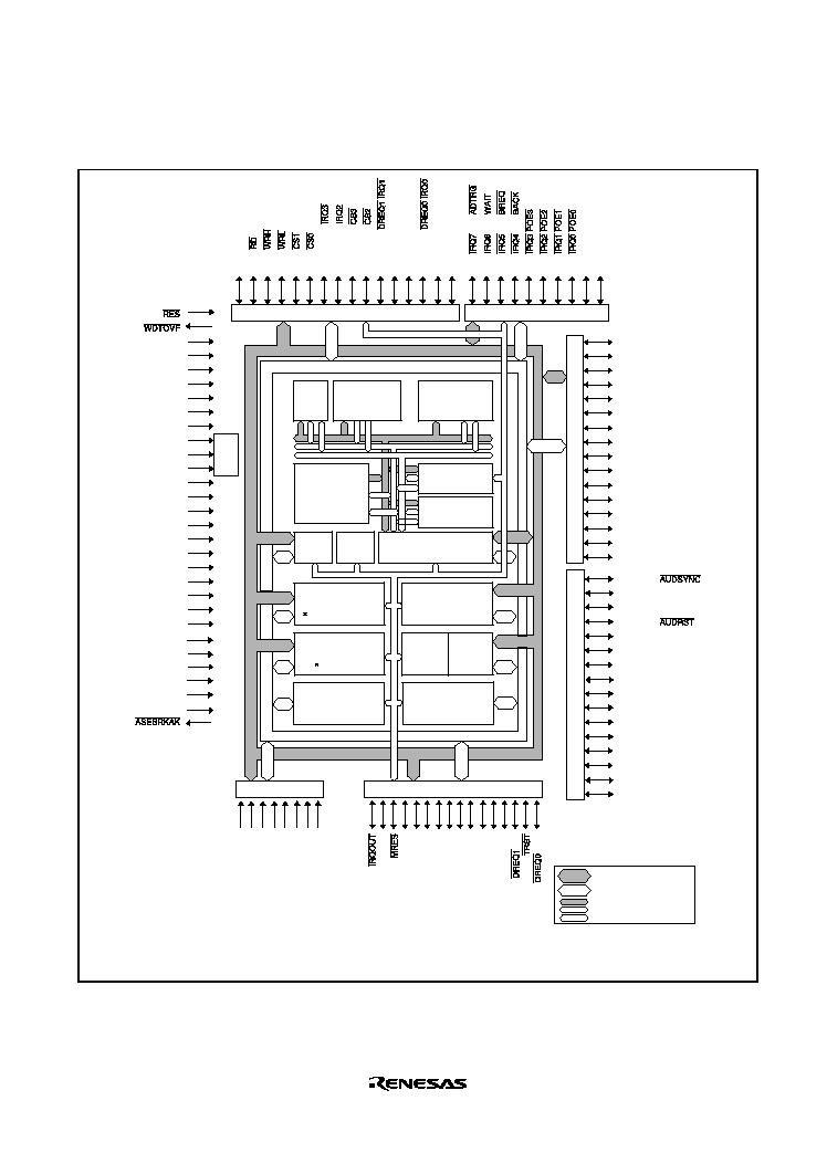
Rev. 2.0, 09/02, page 3 of 732
1.2
Internal Block Diagram
PE15/TIOC4D/DACK1/
PE14/TIOC4C/DACK0
PE13/TIOC4B/
PE12/TIOC4A/TXD3
PE11/TIOC3D/RXD3
PE10/TIOC3C/TXD2
PE9/TIOC3B/SCK3
PE8/TIOC3A/SCK2
PE7/TIOC2B/RXD2
PE6/TIOC2A/SCK3
PE5/TIOC1B/TXD3
PE4/TIOC1A/RXD3/TCK
PE3/TIOC0D/DRAK1/TDO
PE2/TIOC0C/
/TDI
PE1/TIOC0B/DRAK0/
PE0/TIOC0A/
/TMS
;;
;
;
Peripheral address bus (12bits)
Peripheral data bus (16bits)
Internal address bus (32bits)
Internal upper data bus (16bits)
Internal lower data bus (16bits)
MD3
MD2
MD1
MD0
NMI
EXTAL
XTAL
PLLVcc
PLLCAP
PLLVss
FWP
*
Vcc
Vcc
Vcc
Vss
Vss
Vss
Vss
Vss
Vss
Vss
Vss
Vss
Vss
AVcc
AVss
DBGMD
;
;
;;
;
;;
Serial communication
interface
( 4 channels)
Compare match
timer
( 2 channels)
I
2
C bus interface
Interrupt
controller
User break
controller
Bus state
controller
A/D
converter
Watchdog
timer
Multifunction
timer pulse unit
;
;
;
;
CPU
Data transfer
Controller
Direct memory
access controller
RAM
8kB
;
;
;
;
;;;;
;;;;
;
;
;
;;;;
;;;;
;;;;
;;;;
;
;;
;;
;;
;;
;
;
;
;
;
;
;
;
;
P
L
L
;
;
;
;
;;
;
;
;
PD15/D15/
PD14/D14/AUDCK
PD13/D13/AUDMD
PD12/D12/
PD11/D11/AUDATA3
PD10/D10/AUDATA2
PD9/D9/AUDATA1
PD8/D8/AUDATA0
PD7/D7
PD6/D6
PD5/D5
PD4/D4
PD3/D3
PD2/D2
PD1/D1
PD0/D0
PF7/AN7
PF6/AN6
PF5/AN5
PF4/AN4
PF3/AN3
PF2/AN2
PF1/AN1
PF0/AN0
H-UDI
*
;
;
PB9/
/A21/
PB8/
/A20/
PB7/
/A19/
PB6/
/A18/
PB5/
/
PB4/
/
PB3/
/
/SDA0
PB2/
/
/SCL0
PB1/A17
PB0/A16
PC15/A15
PC14/A14
PC13/A13
PC12/A12
PC11/A11
PC10/A10
PC9/A9
PC8/A8
PC7/A7
PC6/A6
PC5/A5
PC4/A4
PC3/A3
PC2/A2
PC1/A1
PC0/A0
PA15/CK
PA14/
PA13/
PA12/
PA11/
PA10/
PA9/TCLKD/
PA8/TCLKC/
PA7/TCLKB/
PA6/TCLKA/
PA5/SCK1/
/
PA4/TXD1
PA3/RXD1
PA2/SCK0/
/
PA1/TXD0
PA0/RXD0
AUD
*
Flash ROM/
mask ROM
256kB
Note: Modules for the F-ZTAT reision only
Figure 1.1 Internal Block Diagram of SH7144
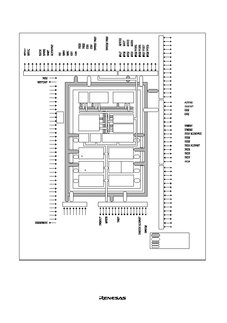
Rev. 2.0, 09/02, page 4 of 732
PE15/TIOC4D/DACK1/
PE14/TIOC4C/DACK0
PE13/TIOC4B/
PE12/TIOC4A/TXD3/TCK
PE11/TIOC3D/RXD3/TDO
PE10/TIOC3C/TXD2/TDI
PE9/TIOC3B/SCK3/
PE8/TIOC3A/SCK2/TMS
PE7/TIOC2B/RXD2
PE6/TIOC2A/SCK3/AUDATA0
PE5/TIOC1B/TXD3/AUDATA1
PE4/TIOC1A/RXD3/AUDATA2
PE3/TIOC0D/DRAK1/AUDATA3
PE2/TIOC0C/
/
PE1/TIOC0B/DRAK0/AUDMD
PE0/TIOC0A/
/AUDCK
;
;
;
MD3
MD2
MD1
MD0
NMI
EXTAL
XTAL
PLLVcc
PLLCAP
PLLVss
FWP
*
Vcc
Vcc
Vcc
Vcc
Vcc
Vcc
Vcc
Vss
Vss
Vss
Vss
Vss
Vss
Vss
Vss
Vss
Vss
Vss
Vss
Vss
AVcc
AVref
AVss
DBGMD
;
;
;
;
;;
;
;
;
;
CPU
RAM
8kB
;
;
;
;
;;;;
;;;;
;
;
;
;;;;
;;;;
;;;;
;;;;
;
;;;
;;;
;
;
;
;
;
;
;
;
;
;;
;;
P
L
L
;
;
;;
;;
;;;
;
;
;
PD31/D31/
PD30/D30/
PD29/D29/
PD28/D28/
PD27/D27/DACK1
PD26/D26/DACK0
PD25/D25/
PD24/D24/
PD23/D23/
/
PD22/D22/
/AUDCK
PD21/D21/
/AUDMD
PD20/D20/
/
PD19/D19/
/AUDATA3
PD18/D18/
/AUDATA2
PD17/D17/
/AUDATA1
PD16/D16/
/AUDATA0
PF7/AN7
PF6/AN6
PF5/AN5
PF4/AN4
PF3/AN3
PF2/AN2
PF1/AN1
PF0/AN0
H-UDI
*
;
;
PD15/D15
PD14/D14
PD13/D13
PD12/D12
PD11/D11
PD10/D10
PD9/D9
PD8/D8
PD7/D7
PD6/D6
PD5/D5
PD4/D4
PD3/D3
PD2/D2
PD1/D1
PD0/D0
PB9/
/A21/
PB8/
/A20/
PB7/
/A19/
PB6/
/A18/
PB5/
/
PB4/
/
PB3/
/
/SDA0
PB2/
/
/SCL0
PB1/A17
PB0/A16
PC15/A15
PC14/A14
PC13/A13
PC12/A12
PC11/A11
PC10/A10
PC9/A9
PC8/A8
PC7/A7
PC6/A6
PC5/A5
PC4/A4
PC3/A3
PC2/A2
PC1/A1
PC0/A0
PA23/
PA22/
PA21
PA20
PA19/
/DRAK1
PA18/
/DRAK0
PA17/
PA16/
PA15/CK
PA14/
PA13/
PA12/
PA11/
PA10/
PA9/TCLKD/
PA8/TCLKC/
PA7/TCLKB/
PA6/TCLKA/
PA5/SCK1/
/
PA4/TXD1
PA3/RXD1
PA2/SCK0/
/
PA1/TXD0
PA0/RXD0
AUD
*
Note: Modules for the F-ZTAT reision only
Serial communication
interface
( 4 channels)
Compare match
timer
( 2 channels)
I
2
C bus interface
Interrupt
controller
User break
controller
Bus state
controller
A/D
converter
Watchdog
timer
Multifunction
timer pulse unit
Data transfer
Controller
Direct memory
access controller
Flash ROM/
mask ROM
256kB
Peripheral address bus (12bits)
Peripheral data bus (16bits)
Internal address bus (32bits)
Internal upper data bus (16bits)
Internal lower data bus (16bits)
Figure 1.2 Block Diagram of SH7145
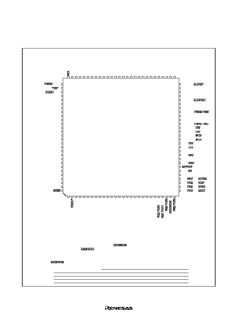
Rev. 2.0, 09/02, page 5 of 732
1.3
Pin Arrangement
84 83 82 81 80 79 78 77 76 75 74 73 72 71 70 69 68 67 66 65 64 63 62 61 60 59 58 57
1
2
3
4
5
6
7
8
9
10 11 12 13 14 15 16 17 18 19 20 21 22 23 24 25 26 27 28
85
86
87
88
89
90
91
92
93
94
95
96
97
98
99
100
101
102
103
104
105
106
107
108
109
110
111
112
56
55
54
53
52
51
50
49
48
47
46
45
44
43
42
41
40
39
38
37
36
35
34
33
32
31
30
29
PD12/D12/
*
4
Vss
PD13/D13/AUDMD
*
4
PD14/D14/AUDCK
*
4
PD15/D15/
*
4
PA0/RXD0
PA1/TXD0
PA2/SCK0/
/
PA3/RXD1
PA4/TXD1
PA5/SCK1/
/
PA6/TCLKA/
PA7/TCLKB/
PA8/TCLKC/
PA9/TCLKD/
PA10/
PA11/
Vss
PA12/
Vcc
PA13/
PA14/
Vss(DBGMD
*
3
)
PB9/
/A21/
PB8/
/A20/
PB7/
/A19/
PB6/
/A18/
PE14/TIOC4C/DACK0
PE15/TIOC4D/DACK1/
Vss
PC0/A0
PC1/A1
PC2/A2
PC3/A3
PC4/A4
PC5/A5
PC6/A6
PC7/A7
PC8/A8
PC9/A9
PC10/A10
PC11/A11
PC12/A12
PC13/A13
PC14/A14
PC15/A15
PB0/A16
Vcc
PB1/A17
Vss
PB2/
/
/SCL0
PB3/
/
/SDA0
PB4/
/
*
2
PB5/
/
PA15/CK
PLLVss
PLLCAP
PLLVcc
MD0
MD1
Vcc(FWP
*
1
)
NMI
MD2
EXTAL
MD3
XTAL
Vss
PD0/D0
PD1/D1
PD2/D2
PD3/D3
PD4/D4
Vcc
PD5/D5
PD6/D6
PD7/D7
Vss
PD8/D8/AUDATA0
*
4
PD9/D9/AUDATA1
*
4
PD10/D10/AUDATA2
*
4
PD11/D11/AUDATA3
*
4
PE0/TIOC0A/
/TMS
*
4
PE1/TIOC0B/DRAK0/
*
4
PE2/TIOC0C/
/TDI
*
4
PE3/TIOC0D/DRAK1/TDO
*
4
PE4/TIOC1A/RXD3/TCK
*
4
Vss
PF0/AN0
PF1/AN1
PF2/AN2
PF3/AN3
PF4/AN4
PF5/AN5
AVss
PF6/AN6
PF7/AN7
AVcc
Vss
PE5/TIOC1B/TXD3
Vcc
PE6/TIOC2A/SCK3
PE7/TIOC2B/RXD2
PE8/TIOC3A/SCK2
PE9/TIOC3B/SCK3
PE10/TIOC3C/TXD2
Vss
PE11/TIOC3D/RXD3
PE12/TIOC4A/TXD3
PE13/TIOC4B/
QFP-112
(Top view)
Notes : 1. Fixed as Vcc in the Mask version, and Used as an FWP pin in the F-ZTAT version (Used as an FWE in write made).
2. Used for E10A debugging mode. Used as an
pin in the F-ZTAT version. Refer to the table below for
processing the
pin.
3. Used for E10A debugging mode. Fixed to Vss in the mask version, or used as a DBGMD pin in the F-ZTAT version.
4. Valid only in the F-ZTAT version (invalid only in the mask version).
Product type
Mask version
F-ZTAT version (when using E10A)
F-ZTAT version (Not when using E10A)
Processing
Fixed to Vcc
Yes
No
Yes
Fixed to Vss
Yes
No
Yes
Pull-up
Yes
Yes
Yes
Pull-down
Yes
No
Yes
NC
No
No
No
Processing
Figure 1.3 SH7144 Pin Arrangement
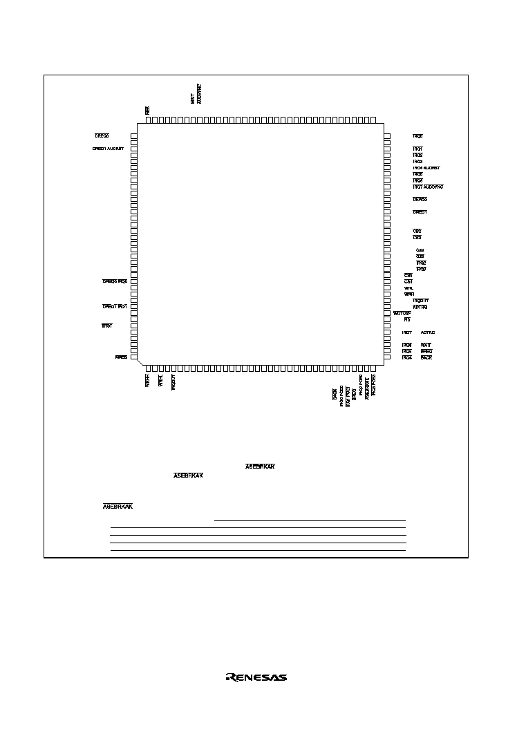
Rev. 2.0, 09/02, page 6 of 732
LQFP-144
(Top view)
PA23/
PE14/TIOC4C/DACK0
PA22/
PA21
PE15/TIOC4D/DACK1/
Vss
PC0/A0
PC1/A1
PC2/A2
PC3/A3
PC4/A4
Vcc
PC5/A5
Vss
PC6/A6
PC7/A7
PC8/A8
PC9/A9
PC10/A10
PC11/A11
PC12/A12
PC13/A13
PC14/A14
PC15/A15
PB0/A16
Vcc
PB1/A17
Vss
PA20
PA19/
/DRAK1
PB2/
/
/SCL0
PB3/
/
/SDA0
PA18/
/DRAK0
PB4/
/
*
2
PB5/
/
109
110
111
112
113
114
115
116
117
118
119
120
121
122
123
124
125
126
127
128
129
130
131
132
133
134
135
136
137
138
139
140
141
142
143
144
PA15/CK
PLLVss
PLLCAP
PLLVcc
MD0
MD1
PA17/
PA16/
*
4
Vcc(FWP
*
1
)
NMI
MD2
EXTAL
MD3
XTAL
Vss
PD0/D0
PD1/D1
PD2/D2
PD3/D3
PD4/D4
Vss
PD5/D5
Vcc
PD6/D6
PD7/D7
PD8/D8
PD9/D9
PD10/D10
Vss
PD11/D11
Vcc
PD12/D12
PD13/D13
PD14/D14
PD15/D15
PE0/TIOC0A/
/AUDCK
*
4
PE1/TIOC0B/DRAK0/AUDMD
*
4
PE2/TIOC0C/
/
*
4
Vcc
PE3/TIOC0D/DRAK1/AUDATA3
*
4
PE4/TIOC1A/RXD3/AUDATA2
*
4
PE5/TIOC1B/TXD3/AUDATA1
*
4
PE6/TIOC2A/SCK3/AUDATA0
*
4
Vss
PF0/AN0
PF1/AN1
PF2/AN2
PF3/AN3
PF4/AN4
PF5/AN5
AVss
PF6/AN6
PF7/AN7
AVref
AVcc
Vss
PA0/RXD0
PA1/TXD0
PA2/SCK0/
/
PA3/RXD1
PA4/TXD1
Vcc
PA5/SCK1/
/
PE7/TIOC2B/RXD2
PE8/TIOC3A/SCK2/TMS
*
4
PE9/TIOC3B/
*
4
/SCK3
PE10/TIOC3C/TXD2/TDI
*
4
Vss
PE11/TIOC3D/TDO
*
4
/RXD3
PE12/TIOC4A/TCK
*
4
/TXD3
PE13/TIOC4B/
PD16/D16/
/AUDATA0
*
4
Vss
PD17/D17/
/AUDATA1
*
4
PD18/D18/
/AUDATA2
*
4
PD19/D19/
/AUDATA3
*
4
PD20/D20/
/
*
4
PD21/D21/
/AUDMD
*
4
PD22/D22/
/AUDCK
*
4
PD23/D23/
/
*
4
Vcc
PD24/D24/
Vss
PD25/D25/
PD26/D26/DACK0
PD27/D27/DACK1
PD28/D28/
PD29/D29/
Vss
PA6/TCLKA/
PA7/TCLKB/
PA8/TCLKC/
PA9/TCLKD/
PA10/
PA11/
PA12/
PA13/
PD30/D30/
PD31/D31/
PA14/
Vss(DBGMD
*
3
)
PB9/
/A21/
Vcc
PB8/
/A20/
PB7/
/A19/
PB6/
/A18/
1
2
3
4
5
6
7
8
9 10 11 12 13 14 15 16 17 18 19 20 21 22 23 24 25 26 27 28 29 30 31 32 33 34 35 36
108 107106 105 104 103102 101 100 99 98 97 96 95 94 93 92 91 90 89 88 87 86 85 84 83 82 81 80 79 78 77 76 75 74 73
72
71
70
69
68
67
66
65
64
63
62
61
60
59
58
57
56
55
54
53
52
51
50
49
48
47
46
45
44
43
42
41
40
39
38
37
Notes : 1. Fixed as Vcc in the Mask version, and Used as an FWP pin in the F-ZTAT version (Used as an FWE in write made).
2. Used for E10A debugging mode. Used as an
pin in the F-ZTAT version. Refer to the table below for
processing the
pin.
3. Used for E10A debugging mode. Fixed to Vss in the mask version, or as a DBGMD pin in the F-ZTAT version.
4. Valid only in the F-ZTAT version (invalid only in the mask version).
Product type
Mask version
F-ZTAT version (when using E10A)
F-ZTAT version (Not when using E10A)
Processing
Fixed to Vcc
Yes
No
Yes
Fixed to Vss
Yes
No
Yes
Pull-up
Yes
Yes
Yes
Pull-down
Yes
No
Yes
NC
No
No
No
Processing
Figure 1.4 SH7145 Pin Arrangement

Rev. 2.0, 09/02, page 7 of 732
1.4
Pin Functions
Type
Symbol
I/O
Name
Function
V
CC
Input
Power supply
Power supply pins. Connect all these pins
to the system power supply. The chip does
not operate when some of these pins are
opened.
Power
Supply
V
SS
Input
Ground
Ground pins. Connect all these pins to the
system power supply (0 V). The chip does
not operate when some of these pins are
opened.
PLLV
CC
Input
Power supply
for PLL
Power supply pin for supplying power to
on-chip PLL.
PLLV
SS
Input
Ground for
PLL
On-chip PLL oscillator ground pin.
PLLCAP
Input
Capacitance
for PLL
External capacitance pin for an on-chip
PLL oscillator.
EXTAL
Input
External clock
For connection to a crystal resonator. (An
external clock can be supplied from the
EXTAL pin.) For examples of crystal
resonator connection and external clock
input, see section 4, Clock Pulse
Generator.
XTAL
Input
Crystal
For connection to a crystal resonator. For
examples of crystal resonator connection
and external clock input, see section 4,
Clock Pulse Generator.
Clock
CK
Output
System clock
output
Supplies the system clock to external
devices.
MD3
MD2
MD1
MD0
Input
Set the mode
Set the operating mode. Inputs at these
pins should not be changed during
operation.
Operating
mode control
FWP
Input
Protection
against write
operation into
Flash memory
Pin for the flash memory. This pin is only
used in the F-ZTAT version. Programming
or erasing of flash memory can be
protected. This pin is used as Vcc in the
mask ROM version.

Rev. 2.0, 09/02, page 8 of 732
Type
Symbol
I/O
Name
Function
RES
Input
Power on
reset
When this pin is driven low, the chip
becomes to power on reset state.
MRES
Input
Manual reset
When this pin is driven low, the chip
becomes to manual reset state.
WDTOVF*
Output
Watchdog
timer overflow
Output signal for the watchdog timer
overflow.
If this pin needs to be pulled-down, the
resistance value must be 1 M
or higher.
BREQ
Input
Bus request
External device can request the release of
the bus mastership by setting this pin low.
System
control
BACK
Output
Bus
acknowledge
Shows that the bus mastership has been
released for the external device. The
device that had issued the
BREQ
signal
can know that bus mastership has been
released for itself by receiving the
BACK
signal.
NMI
Input
Non-maskable
interrupt
Non-maskable interrupt pin. If this pin is
not used, it should be fixed high.
IRQ7
IRQ3
IRQ6
IRQ2
IRQ5
IRQ1
IRQ4
IRQ0
Input
Interrupt
request 7 to 0
These pins request a maskable interrupt.
One of the level input or edge input can be
selected In case of the edge input, one of
the rising edge, falling edge, or both can
be selected.
Interrupts
IRQOUT
Output
Interrupt
request output
Shows that an interrupt cause has
occurred. The interrupt cause can be
recognized even in the bus release state.
Address bus
A21 to A0
Output
Address bus
Output the address.
Data bus
SH7144:
D15 to D0
SH7145:
D31 to D0
Input/
Output
Data bus
SH7144: Bi-directional 16-bit bus
SH7145: Bi-directional 32-bit bus
CS3
CS1
CS2
CS0
Output
Chip select
3 to 0
Chip select signal for external memory or
devices.
RD
Output
Read
Shows reading from external devices.
WRHH
(SH7145
only)
Output
Write HH
Shows writing into the HH 8 bits (bits 31 to
24) of the external data.
Bus control
WRHL
(SH7145
only)
Output
Write HL
Shows writing into the HL 8 bits (bits 23 to
16) of the external data.

Rev. 2.0, 09/02, page 9 of 732
Type
Symbol
I/O
Name
Function
WRH
Output
Write
upper half
Shows writing into the upper 8 bits (bits 15
to 8) of the external data.
WRL
Output
Write lower
half
Shows writing into the lower 8 bits (bit7 to
bit0) of the external data.
Bus control
WAIT
Input
Wait
Inserts the wait cycles into the bus cycle
when accessing the external spaces.
DREQ0
DREQ1
Input
DMA transfer
request
DMA request input pins from an external
device.
DRAK0
DRAK1
Output
DREQ request
acknowledge
Outputs an acknowledge signal to the
external device that has input a DMA
transfer request signal.
Direct
memory
access
controller
(DMAC)
DACK0
DACK1
Output
DMA transfer
strobe
Outputs a strobe to the I/O of the external
device that has input a DMA transfer
request signal.
TCLKA
TCLKB
TCLKC
TCLKD
Input
External clock
input for MTU
timer
These pins input an external clock.
TIOC0A
TIOC0B
TIOC0C
TIOC0D
Input/
Output
MTU input
capture/output
compare
(channel 0)
The TGRA_0 to TGRD_0 input capture
input/output compare output/PWM output
pins.
TIOC1A
TIOC1B
Input/
Output
MTU input
capture/output
compare
(channel 1)
The TGRA_1 to TGRB_1 input capture
input/output compare output/PWM output
pins.
TIOC2A
TIOC2B
Input/
Output
MTU input
capture/output
compare
(channel 2)
The TGRA_2 to TGRB_2 input capture
input/output compare output/PWM output
pins.
TIOC3A
TIOC3B
TIOC3C
TIOC3D
Input/
Output
MTU input
capture/output
compare
(channel 3)
The TGRA_3 to TGRD_3 input capture
input/output compare output/PWM output
pins.
Multi function
timer-pulse
unit (MTU)
TIOC4A
TIOC4B
TIOC4C
TIOC4D
Input/
Output
MTU input
capture/output
compare
(channel 4)
The TGRA_4 to TGRB_4 input capture
input/output compare output/PWM output
pins.

Rev. 2.0, 09/02, page 10 of 732
Type
Symbol
I/O
Name
Function
TXD3 to
TXD0
Output
Transmitted
data
Data output pins.
RXD3 to
RXD0
Input
Received data Data input pins.
Serial
communication
interface (SCI)
SCK3 to
SCK0
Input/
Output
Serial clock
Clock input/output pins.
SCL0
Input/
Output
I
2
C clock
input/ output
I
2
C bus clock input/output pins, which drive
a bus.
Output a clock in the NMOS open-drain
method.
I
2
C bus
interface
(option)
SDA0
Input/
Output
I
2
C data
input/ output
I
2
C bus data input/output pins, which drive
a bus.
Output data in the NMOS open-drain
method.
Output control
for MTU
POE3
to
POE0
Input
Port output
control
Input pins for the signal to request the
output pins of MTU waveforms to become
high impedance state.
AN7 to AN0 Input
Analog input
pins
Analog input pins.
ADTRG
Input
Input of trigger
for A/D
conversion
Pin for input of an external trigger to start
A/D conversion
AVref
(SH7145
only)
Input
Analog
reference
power supply
Analog reference power supply pin, (In
SH7144, this pin is internally connected to
the AVcc pin).
AV
CC
Input
Analog power
supply
Power supply pin for the A/D converter.
When the A/D converter is not used,
connect this pin to the system power
supply (+3.3 V).
A/D
converter
AV
SS
Input
Analog ground The ground pin for the A/D converter.
Connect this pin to the system power
supply (0 V).
SH7144
PA15 to PA0
SH7145
PA23 to PA0
Input/
Output
General
purpose port
SH7144: 16-bit general purpose
input/output pins.
SH7145: 24-bit general purpose
input/output pins.
PB9 to PB0
Input/
Output
General
purpose port
10-bit general purpose input/output pins.
I/O port
PC15 to
PC0
Input/
Output
General
purpose port
16-bit general purpose input/output pins.

Rev. 2.0, 09/02, page 11 of 732
Type
Symbol
I/O
Name
Function
SH7144:
PD15 to
PD0
SH7145:
PD31 to
PD0
Input/
Output
General
purpose port
SH7144: 16-bit general purpose
input/output pins.
SH7145: 32-bit general purpose
input/output pins.
PE15 to PE0 Input/
Output
General
purpose port
16-bit general purpose input/output pins.
I/O port
PF7 to PF0
Input
General
purpose port
8-bit general purpose input pins.
TCK
Input
Test clock
Test clock input pin.
TMS
Input
Test mode
select
Test mode select signal input pin.
TDI
Input
Test data
input
Instruction/data serial input pin.
TDO
Output
Test data
output
Instruction/data serial output pin.
Hitachi user
debug
interface
(H-UDI)
(flash version
only)
TRST
Input
Test reset
Initialization signal input pin.
AUDATA3 to
AUDATA0
Input/
Output
AUD data
Branch trace mode: Branch destination
address output pins.
RAM monitor mode: Monitor address
input/data input/output pins.
AUDRST
Input
AUD reset
Reset signal input pin.
AUDMD
Input
AUD mode
Mode select signal input pin.
Branch trace mode: Low
RAM monitor mode: High
AUDCK
Input/
Output
AUD clock
Branch trace mode: Synchronous clock
output pin.
RAM monitor mode: Synchronous clock
input pin.
Advanced user
debugger
(AUD)
(flash version
only)
AUDSYNC
Input/
Output
AUD
synchroniza-
tion signal
Branch trace mode: Data start position
identification signal output pin.
RAM monitor mode: Data start position
identification signal input pin.

Rev. 2.0, 09/02, page 12 of 732
Type
Symbol
I/O
Name
Function
ASEBRKAK
Output
Break mode
acknowledge
Shows that E10A has entered to the break
mode. Refer to "E10A emulator user's
manual for SH7144 (provisional name)" for
the detail of the connection to E10A.
E10 interface
(flash version
only)
DBGMD
Input
Debug mode
Enables the functions of E10A emulator.
Input low to the pin in normal operation
(other than the debug mode). In debug
mode, input high to the pin on the user
board. Refer to "E10A emulator user's
manual for SH7144 (provisional name)" for
the detail of the connection to E10A.
Note:
*
Do not pull-down the
WDTOVF
pin. If this pin needs to be pulled-down, however, the
resistance value must be 1 M
or higher.

CPUS201A_010020020700
Rev. 2.0, 09/02, page 13 of 732
Section 2 CPU
2.1
Features
∑
General-register architecture
Sixteen 32-bit general registers
∑
Sixty-two basic instructions
∑
Eleven addressing modes
Register direct [Rn]
Register indirect [@Rn]
Register indirect with post-increment [@Rn+]
Register indirect with pre-decrement [@-Rn]
Register indirect with displacement [@disp:4,Rn]
Register indirect with index [@R0, Rn]
GBR indirect with displacement [@disp:8,GBR]
GBR indirect with index [@R0,GBR]
Program-counter relative with displacement [@disp:8,PC]
Program-counter relative [disp:8/disp:12/Rn]
Immediate [#imm:8]
2.2
Register Configuration
The register set consists of sixteen 32-bit general registers, three 32-bit control registers, and four
32-bit system registers.
2.2.1
General Registers (Rn)
The sixteen 32-bit general registers (Rn) are numbered R0 to R15. General registers are used for
data processing and address calculation. R0 is also used as an index register. Several instructions
have R0 fixed as their only usable register. R15 is used as the hardware stack pointer (SP). Saving
and recovering the status register (SR) and program counter (PC) in exception processing is
accomplished by referencing the stack using R15.
Rev. 2.0, 09/02, page 14 of 732
31
0
R0
*
1
R1
R2
R3
R4
R5
R6
R7
R8
R9
R10
R11
R12
R13
R14
R15, SP (hardware stack pointer)
*
2
General registers (Rn)
Status register (SR)
Global base register (GBR)
Vector base register (VBR)
Multiply-accumulate register (MAC)
Procedure register
Program counter (PC)
31
9 8 7 6 5 4 3 2 1 0
0
0
31
M
GBR
31
VBR
Q I3 I2 I1 I0
S T
31
0
MACH
31
0
PR
31
0
PC
MACL
Notes: 1. R0 functions as an index register in the indirect indexed register addressing mode and indirect indexed GBR
addressing mode. In some instructions, R0 functions as a fixed source register or destination register.
2. R15 functions as a hardware stack pointer (SP) during exception processing.
Figure 2.1 CPU Internal Registers

Rev. 2.0, 09/02, page 15 of 732
2.2.2
Control Registers
The control registers consist of three 32-bit registers: status register (SR), global base register
(GBR), and vector base register (VBR). The status register indicates processing states. The global
base register functions as a base address for the indirect GBR addressing mode to transfer data to
the registers of on-chip peripheral modules. The vector base register functions as the base address
of the exception processing vector area (including interrupts).
Status Register (SR):
Bit
Bit Name
Initial Value
R/W
Description
31
30
29
28
27
26
25
24
23
22
21
20
19
18
17
16
15
14
13
12
11
10
--
--
--
--
--
--
--
--
--
--
--
--
--
--
--
--
--
--
--
--
--
--
0
0
0
0
0
0
0
0
0
0
0
0
0
0
0
0
0
0
0
0
0
0
R/W
R/W
R/W
R/W
R/W
R/W
R/W
R/W
R/W
R/W
R/W
R/W
R/W
R/W
R/W
R/W
R/W
R/W
R/W
R/W
R/W
R/W
Reserved bits.
This bit is always read as 0. The write value should
always be 0.
9
M
Undefined
R/W
Used by the DIV0U, DIV0S, and DIV1 instructions.
8
Q
Undefined
R/W
Used by the DIV0U, DIV0S, and DIV1 instructions.

Rev. 2.0, 09/02, page 16 of 732
Bit
Bit Name
Initial Value
R/W
Description
7
6
5
4
I3
I2
I1
I0
1
1
1
1
R/W
R/W
R/W
R/W
Interrupt mask bits.
3
2
--
--
0
0
R/W
R/W
Reserved bits. This bit is always read as 0.
The write value should always be 0.
1
S
Undefined
R/W
S bit
Used by the MAC instruction.
0
T
Undefined
R/W
T bit
The MOVT, CMP/cond, TAS, TST, BT (BT/S), BF
(BF/S), SETT, and CLRT instructions use the T bit to
indicate true (1) or false (0).
The ADDV, ADDC, SUBV, SUBC, DIV0U, DIV0S,
DIV1, NEGC, SHAR, SHAL, SHLR, SHLL, ROTR,
ROTL, ROTCR, and ROTCL instructions also use the
T bit to indicate carry/borrow or overflow/underflow.
Global Base Register (GBR): Indicates the base address of the indirect GBR addressing mode.
The indirect GBR addressing mode is used in data transfer for on-chip peripheral modules register
areas and in logic operations.
Vector Base Register (VBR): Indicates the base address of the exception processing vector area.
2.2.3
System Registers
System registers consist of four 32-bit registers: high and low multiply and accumulate registers
(MACH and MACL), the procedure register (PR), and the program counter (PC).
Multiply-and-Accumulate Registers (MAC): Registers to store the results of multiply-and-
accumulate operations.
Procedure Register (PR): Registers to store the return address from a subroutine procedure.
Program Counter (PC): Registers to indicate the sum of current instruction addresses and four,
that is, the address of the second instruction after the current instruction.

Rev. 2.0, 09/02, page 17 of 732
2.2.4
Initial Values of Registers
Table 2.1 lists the values of the registers after reset.
Table 2.1 Initial Values of Registers
Classification
Register
Initial Value
R0 to R14
Undefined
General registers
R15 (SP)
Value of the stack pointer in the vector
address table
SR
Bits I3 to I0 are 1111 (H'F), reserved bits
are 0, and other bits are undefined
GBR
Undefined
Control registers
VBR
H'00000000
MACH, MACL, PR
Undefined
System registers
PC
Value of the program counter in the vector
address table
2.3
Data Formats
2.3.1
Data Format in Registers
Register operands are always longwords (32 bits). If the size of memory operand is a byte (8 bits)
or a word (16 bits), it is changed into a longword by expanding the sign-part when loaded into a
register.
31
0
Longword
Figure 2.2 Data Format in Registers
2.3.2
Data Formats in Memory
Memory data formats are classified into bytes, words, and longwords. Byte data can be accessed
from any address. Locate, however, word data at an address 2n, longword data at 4n. Otherwise,
an address error will occur if an attempt is made to access word data starting from an address other
than 2n or longword data starting from an address other than 4n. In such cases, the data accessed
cannot be guaranteed. The hardware stack area, pointed by the hardware stack pointer (SP, R15),
uses only longword data starting from address 4n because this area holds the program counter and
status register.

Rev. 2.0, 09/02, page 18 of 732
31
0
15
23
7
Byte
Byte
Byte
Byte
Word
Word
Address 2n
Address 4n
Longword
Address m
Address m + 2
Address m + 1
Address m + 3
Figure 2.3 Data Formats in Memory
2.3.3
Immediate Data Format
Byte (8 bit) immediate data resides in an instruction code. Immediate data accessed by the MOV,
ADD, and CMP/EQ instructions is sign-extended and handled in registers as longword data.
Immediate data accessed by the TST, AND, OR, and XOR instructions is zero-extended and
handled as longword data. Consequently, AND instructions with immediate data always clear the
upper 24 bits of the destination register.
Word or longword immediate data is not located in the instruction code, but instead is stored in a
memory table. An immediate data transfer instruction (MOV) accesses the memory table using the
PC relative addressing mode with displacement.
2.4
Instruction Features
2.4.1
RISC-Type Instruction Set
All instructions are RISC type. This section details their functions.
16-Bit Fixed Length: All instructions are 16 bits long, increasing program code efficiency.
One Instruction per State: The microcomputer can execute basic instructions in one state using
the pipeline system. One state is 25 ns at 40 MHz.
Data Length: Longword is the standard data length for all operations. Memory can be accessed in
bytes, words, or longwords. Byte or word data accessed from memory is sign-extended and
handled as longword data. Immediate data is sign-extended for arithmetic operations or zero-
extended for logic operations. It also is handled as longword data.

Rev. 2.0, 09/02, page 19 of 732
Table 2.2 Sign Extension of Word Data
CPU of This LSI
Description
Example of Conventional CPU
MOV.W @(disp,PC),R1
ADD R1,R0
.........
.DATA.W H'1234
Data is sign-extended to 32
bits, and R1 becomes
H'00001234. It is next
operated upon by an ADD
instruction.
ADD.W #H'1234,R0
Note:
@(disp, PC) accesses the immediate data.
Load-Store Architecture: Basic operations are executed between registers. For operations that
involve memory access, data is loaded to the registers and executed (load-store architecture).
Instructions such as AND that manipulate bits, however, are executed directly in memory.
Delayed Branch Instructions: Unconditional branch instructions are delayed branch instructions.
With a delayed branch instruction, the branch is taken after execution of the instruction following
the delayed branch instruction. This reduces the disturbance of the pipeline control in case of
branch instructions. There are two types of conditional branch instructions: delayed branch
instructions and ordinary branch instructions.
Table 2.3 Delayed Branch Instructions
CPU of This LSI
Description
Example of Conventional CPU
BRA TRGET
ADD R1,R0
Executes the ADD before
branching to TRGET.
ADD.W R1,R0
BRA TRGET
Multiply/Multiply-and-Accumulate Operations: 16-bit
◊
16-bit
32-bit multiply operations
are executed in one to two states. 16-bit
◊
16-bit + 64-bit
64-bit multiply-and-accumulate
operations are executed in two to three states. 32-bit
◊
32-bit
64-bit multiply and 32-bit
◊
32-bit
+ 64-bit
64-bit multiply-and-accumulate operations are executed in two to four states.
T Bit: The T bit in the status register changes according to the result of the comparison. Whether a
conditional branch is taken or not taken depends upon the T bit condition (true/false). The number
of instructions that change the T bit is kept to a minimum to improve the processing speed.

Rev. 2.0, 09/02, page 20 of 732
Table 2.4 T Bit
CPU of This LSI
Description
Example of Conventional CPU
CMP/GE R1,R0
BT TRGET0
BF TRGET1
T bit is set when R0
R1. The
program branches to TRGET0
when R0
R1 and to TRGET1
when R0 < R1.
CMP.W R1,R0
BGE TRGET0
BLT TRGET1
ADD #
-
1,R0
CMP/EQ #0,R0
BT TRGET
T bit is not changed by ADD.
T bit is set when R0 = 0. The
program branches if R0 = 0.
SUB.W #1,R0
BEQ TRGET
Immediate Data: Byte (8-bit) immediate data is located in an instruction code. Word or longword
immediate data is not located in instruction codes but in a memory table. An immediate data
transfer instruction (MOV) accesses the memory table using the PC relative addressing mode with
displacement.
Table 2.5 Immediate Data Accessing
Classification
CPU of This LSI
Example of Conventional CPU
8-bit immediate
MOV #H'12,R0
MOV.B #H'12,R0
16-bit immediate
MOV.W @(disp,PC),R0
.................
.DATA.W H'1234
MOV.W #H'1234,R0
32-bit immediate
MOV.L @(disp,PC),R0
.................
.DATA.L H'12345678
MOV.L #H'12345678,R0
Note:
@(disp, PC) accesses the immediate data.
Absolute Address: When data is accessed by absolute address, the value in the absolute address is
placed in the memory table in advance. That value is transferred to the register by loading the
immediate data during the execution of the instruction, and the data is accessed in the indirect
register addressing mode.

Rev. 2.0, 09/02, page 21 of 732
Table 2.6 Absolute Address Accessing
Classification
CPU of This LSI
Example of Conventional CPU
Absolute address
MOV.L @(disp,PC),R1
MOV.B @R1,R0
..................
.DATA.L H'12345678
MOV.B @H'12345678,R0
Note:
@(disp,PC) accesses the immediate data.
16-Bit/32-Bit Displacement: When data is accessed by 16-bit or 32-bit displacement, the
displacement value is placed in the memory table in advance. That value is transferred to the
register by loading the immediate data during the execution of the instruction, and the data is
accessed in the indirect indexed register addressing mode.
Table 2.7 Displacement Accessing
Classification
CPU of This LSI
Example of Conventional CPU
16-bit displacement
MOV.W @(disp,PC),R0
MOV.W @(R0,R1),R2
..................
.DATA.W H'1234
MOV.W @(H'1234,R1),R2
Note:
@(disp,PC) accesses the immediate data.
Rev. 2.0, 09/02, page 22 of 732
2.4.2
Addressing Modes
Table 2.8 describes addressing modes and effective address calculation.
Table 2.8 Addressing Modes and Effective Addresses
Addressing
Mode
Instruction
Format
Effective Address Calculation
Equation
Direct register
addressing
Rn
The effective address is register Rn. (The operand
is the contents of register Rn.)
--
Indirect register
addressing
@Rn
The effective address is the contents of register Rn.
Rn
Rn
Rn
Post-increment
indirect register
addressing
@Rn+
The effective address is the contents of register Rn.
A constant is added to the content of Rn after the
instruction is executed. 1 is added for a byte
operation, 2 for a word operation, and 4 for a
longword operation.
Rn
Rn
1/2/4
+
Rn + 1/2/4
Rn
(After the
instruction
executes)
Byte:
Rn + 1
Rn
Word:
Rn + 2
Rn
Longword:
Rn + 4
Rn
Pre-decrement
indirect register
addressing
@-Rn
The effective address is the value obtained by
subtracting a constant from Rn. 1 is subtracted for
a byte operation, 2 for a word operation, and 4 for
a longword operation.
Rn
1/2/4
Rn ≠ 1/2/4
≠
Rn ≠ 1/2/4
Byte:
Rn ≠ 1
Rn
Word:
Rn ≠ 2
Rn
Longword:
Rn ≠ 4
Rn
(Instruction is
executed with
Rn after this
calculation)
Indirect register
addressing with
displacement
@(disp:4,
Rn)
The effective address is the sum of Rn and a 4-bit
displacement (disp). The value of disp is zero-
extended, and remains unchanged for a byte
operation, is doubled for a word operation, and is
quadrupled for a longword operation.
Rn
Rn + disp
◊
1/2/4
+
◊
1/2/4
disp
(zero-extended)
Byte:
Rn + disp
Word:
Rn + disp
◊
2
Longword:
Rn + disp
◊
4
Rev. 2.0, 09/02, page 23 of 732
Addressing
Mode
Instruction
Format
Effective Address Calculation
Equation
Indirect indexed
register
addressing
@(R0, Rn)
The effective address is the sum of Rn and R0.
Rn
R0
Rn + R0
+
Rn + R0
Indirect GBR
addressing with
displacement
@(disp:8,
GBR)
The effective address is the sum of GBR value and
an 8-bit displacement (disp). The value of disp is
zero-extended, and remains unchanged for a byte
operation, is doubled for a word operation, and is
quadrupled for a longword operation.
GBR
1/2/4
GBR
+ disp
◊
1/2/4
+
◊
disp
(zero-extended)
Byte:
GBR + disp
Word:
GBR + disp
◊
2
Longword:
GBR + disp
◊
4
Indirect indexed
GBR addressing
@(R0,
GBR)
The effective address is the sum of GBR value and
R0.
GBR
R0
GBR + R0
+
GBR + R0
Indirect PC
addressing with
displacement
@(disp:8,
PC)
The effective address is the sum of PC value and
an 8-bit displacement (disp). The value of disp is
zero-extended, and is doubled for a word operation,
and quadrupled for a longword operation. For a
longword operation, the lowest two bits of the PC
value are masked.
PC
H'FFFFFFFC
PC + disp
◊
2
or
PC & H'FFFFFFFC
+ disp
◊
4
+
2/4
◊
&
(for longword)
disp
(zero-extended)
Word:
PC + disp
◊
2
Longword:
PC &
H'FFFFFFFC
+ disp
◊
4
Rev. 2.0, 09/02, page 24 of 732
Addressing
Mode
Instruction
Format
Effective Address Calculation
Equation
PC relative
addressing
disp:8
The effective address is the sum of PC value and
the value that is obtained by doubling the sign-
extended 8-bit displacement (disp).
PC
2
+
◊
disp
(sign-extended)
PC + disp
◊
2
PC + disp
◊
2
disp:12
The effective address is the sum of PC value and
the value that is obtained by doubling the sign-
extended 12-bit displacement (disp).
PC
2
+
◊
disp
(sign-extended)
PC + disp
◊
2
PC + disp
◊
2
Rn
The effective address is the sum of the register PC
and Rn.
PC
Rn
PC + Rn
+
PC + Rn
Immediate
addressing
#imm:8
The 8-bit immediate data (imm) for the TST, AND,
OR, and XOR instructions is zero-extended.
--
#imm:8
The 8-bit immediate data (imm) for the MOV, ADD,
and CMP/EQ instructions is sign-extended.
--
#imm:8
The 8-bit immediate data (imm) for the TRAPA
instruction is zero-extended and then quadrupled.
--

Rev. 2.0, 09/02, page 25 of 732
2.4.3
Instruction Format
The instruction formats and the meaning of source and destination operand are described below.
The meaning of the operand depends on the instruction code. The symbols used are as follows:
∑
xxxx: Instruction code
∑
mmmm: Source register
∑
nnnn: Destination register
∑
iiii: Immediate data
∑
dddd: Displacement
Table 2.9 Instruction Formats
Instruction Formats
Source
Operand
Destination
Operand
Example
0 format
xxxx
xxxx
xxxx
xxxx
15
0
--
--
NOP
--
nnnn: Direct
register
MOVT
Rn
Control register or
system register
nnnn: Direct
register
STS
MACH,Rn
n format
xxxx
xxxx
xxxx
nnnn
15
0
Control register or
system register
nnnn: Indirect pre-
decrement register
STC.L SR,@-Rn
mmmm: Direct
register
Control register or
system register
LDC
Rm,SR
mmmm: Indirect
post-increment
register
Control register or
system register
LDC.L @Rm+,SR
mmmm: Indirect
register
--
JMP
@Rm
m format
xxxx
mmmm
xxxx
xxxx
15
0
mmmm: PC relative
using Rm
--
BRAF
Rm

Rev. 2.0, 09/02, page 26 of 732
Instruction Formats
Source
Operand
Destination
Operand
Example
mmmm: Direct
register
nnnn: Direct
register
ADD
Rm,Rn
mmmm: Direct
register
nnnn: Indirect
register
MOV.L Rm,@Rn
mmmm: Indirect
post-increment
register (multiply-
and-accumulate)
nnnn
*
: Indirect
post-increment
register (multiply-
and-accumulate)
MACH, MACL
MAC.W
@Rm+,@Rn+
mmmm: Indirect
post-increment
register
nnnn: Direct
register
MOV.L @Rm+,Rn
mmmm: Direct
register
nnnn: Indirect pre-
decrement
register
MOV.L Rm,@-Rn
nm format
nnnn
xxxx
xxxx
15
0
mmmm
mmmm: Direct
register
nnnn: Indirect
indexed register
MOV.L
Rm,@(R0,Rn)
md format
xxxx
dddd
15
0
mmmm
xxxx
mmmmdddd:
Indirect register with
displacement
R0 (Direct
register)
MOV.B
@(disp,Rn),R0
nd4 format
xxxx
xxxx
dddd
15
0
nnnn
R0 (Direct register)
nnnndddd:
Indirect register with
displacement
MOV.B
R0,@(disp,Rn)
mmmm: Direct
register
nnnndddd: Indirect
register with
displacement
MOV.L
Rm,@(disp,Rn)
nmd format
nnnn
xxxx
dddd
15
0
mmmm
mmmmdddd:
Indirect register with
displacement
nnnn: Direct
register
MOV.L
@(disp,Rm),Rn
Rev. 2.0, 09/02, page 27 of 732
Instruction Formats
Source
Operand
Destination
Operand
Example
dddddddd: Indirect
GBR with
displacement
R0 (Direct register)
MOV.L
@(disp,GBR),R0
R0 (Direct register)
dddddddd: Indirect
GBR with
displacement
MOV.L
R0,@(disp,GBR)
dddddddd: PC
relative with
displacement
R0 (Direct register)
MOVA
@(disp,PC),R0
d format
dddd
xxxx
15
0
xxxx
dddd
--
dddddddd: PC
relative
BF label
d12 format
dddd
xxxx
15
0
dddd
dddd
--
dddddddddddd: PC
relative
BRA label
(label = disp
+ PC)
nd8 format
dddd
nnnn
xxxx
15
0
dddd
dddddddd: PC
relative with
displacement
nnnn: Direct
register
MOV.L
@(disp,PC),Rn
iiiiiiii: Immediate
Indirect indexed
GBR
AND.B
#imm,@(R0,GBR)
iiiiiiii: Immediate
R0 (Direct register)
AND #imm,R0
i format
xxxx
xxxx
i i i i
15
0
i i i i
iiiiiiii: Immediate
--
TRAPA #imm
ni format
nnnn
i i i i
xxxx
15
0
i i i i
iiiiiiii: Immediate
nnnn: Direct
register
ADD #imm,Rn
Note:
In multiply-and-accumulate instructions, nnnn is the source register.

Rev. 2.0, 09/02, page 28 of 732
2.5
Instruction Set
2.5.1
Instruction Set by Classification
Table 2.10 lists the instructions according to their classification.
Table 2.10 Classification of Instructions
Classification Types
Operation
Code
Function
No. of
Instructions
MOV
Data transfer, immediate data transfer,
peripheral module data transfer, structure data
transfer
MOVA
Effective address transfer
MOVT
T bit transfer
SWAP
Swap of upper and lower bytes
Data transfer
5
XTRCT
Extraction of the middle of registers connected
39
21
ADD
Binary addition
33
ADDC
Binary addition with carry
ADDV
Binary addition with overflow check
CMP/cond Comparison
DIV1
Division
Arithmetic
operations
DIV0S
Initialization of signed division
DIV0U
Initialization of unsigned division
DMULS
Signed double-length multiplication
DMULU
Unsigned double-length multiplication
DT
Decrement and test
EXTS
Sign extension
EXTU
Zero extension
MAC
Multiply-and-accumulate, double-length
multiply-and-accumulate operation
MUL
Double-length multiply operation
MULS
Signed multiplication
MULU
Unsigned multiplication
NEG
Negation
NEGC
Negation with borrow
SUB
Binary subtraction

Rev. 2.0, 09/02, page 29 of 732
Classification Types
Operation
Code
Function
No. of
Instructions
SUBC
Binary subtraction with borrow
33
Arithmetic
operations
SUBV
Binary subtraction with underflow
6
AND
Logical AND
14
NOT
Bit inversion
OR
Logical OR
TAS
Memory test and bit set
TST
Logical AND and T bit set
Logic
operations
XOR
Exclusive OR
Shift
10
ROTL
One-bit left rotation
14
ROTR
One-bit right rotation
ROTCL
One-bit left rotation with T bit
ROTCR
One-bit right rotation with T bit
SHAL
One-bit arithmetic left shift
SHAR
One-bit arithmetic right shift
SHLL
One-bit logical left shift
SHLLn
n-bit logical left shift
SHLR
One-bit logical right shift
SHLRn
n-bit logical right shift
Branch
9
BF
Conditional branch, conditional branch with
delay (Branch when T = 0)
11
BT
Conditional branch, conditional branch with
delay (Branch when T = 1)
BRA
Unconditional branch
BRAF
Unconditional branch
BSR
Branch to subroutine procedure
BSRF
Branch to subroutine procedure
JMP
Unconditional branch
JSR
Branch to subroutine procedure
RTS
Return from subroutine procedure

Rev. 2.0, 09/02, page 30 of 732
Classification Types
Operation
Code
Function
No. of
Instructions
11
CLRT
T bit clear
31
System
control
CLRMAC
MAC register clear
LDC
Load to control register
LDS
Load to system register
NOP
No operation
RTE
Return from exception processing
SETT
T bit set
SLEEP
Transition to power-down mode
STC
Store control register data
STS
Store system register data
TRAPA
Trap exception handling
Total:
62
142

Rev. 2.0, 09/02, page 31 of 732
The table below shows the format of instruction codes, operation, and execution states. They are
described by using this format according to their classification.
Instruction Code Format
Item
Format
Explanation
Instruction
Described in
mnemonic.
OP.Sz SRC,DEST
OP: Operation code
Sz: Size
SRC: Source
DEST: Destination
Rm: Source register
Rn: Destination register
imm: Immediate data
disp: Displacement
*
2
Instruction
code
Described in MSB
LSB order
mmmm: Source register
nnnn: Destination register
0000: R0
0001: R1
1111: R15
iiii: Immediate data
dddd: Displacement
,
Direction of transfer
(xx)
Memory operand
M/Q/T
Flag bits in the SR
&
Logical AND of each bit
|
Logical OR of each bit
^
Exclusive OR of each bit
~
Logical NOT of each bit
<<n
n-bit left shift
Outline of the
Operation
>>n
n-bit right shift
Execution
states
--
Value when no wait states are inserted
*
1
T bit
--
Value of T bit after instruction is executed. An em-dash (--)
in the column means no change.
Notes: 1. Instruction execution states: The execution states shown in the table are minimums.
The actual number of states may be increased when (1) contention occurs between
instruction fetches and data access, or (2) when the destination register of the load
instruction (memory
register) equals to the register used by the next instruction.
2. Depending on the operand size, displacement is scaled by
◊
1,
◊
2, or
◊
4. For details,
refer the SH-1/SH-2/SH-DSP Programming Manual.

Rev. 2.0, 09/02, page 32 of 732
Data Transfer Instructions
Instruction
Instruction Code
Operation
Execution
States
T
Bit
MOV
#imm,Rn
1110nnnniiiiiiii
#imm
Sign extension
Rn
1
--
MOV.W
@(disp,PC),Rn
1001nnnndddddddd
(disp
◊
2 + PC)
Sign
extension
Rn
1
--
MOV.L
@(disp,PC),Rn
1101nnnndddddddd
(disp
◊
4 + PC)
Rn
1
--
MOV
Rm,Rn
0110nnnnmmmm0011
Rm
Rn
1
--
MOV.B
Rm,@Rn
0010nnnnmmmm0000
Rm
(Rn)
1
--
MOV.W
Rm,@Rn
0010nnnnmmmm0001
Rm
(Rn)
1
--
MOV.L
Rm,@Rn
0010nnnnmmmm0010
Rm
(Rn)
1
--
MOV.B
@Rm,Rn
0110nnnnmmmm0000
(Rm)
Sign extension
Rn
1
--
MOV.W
@Rm,Rn
0110nnnnmmmm0001
(Rm)
Sign extension
Rn
1
--
MOV.L
@Rm,Rn
0110nnnnmmmm0010
(Rm)
Rn
1
--
MOV.B
Rm,@≠Rn
0010nnnnmmmm0100
Rn≠1
Rn, Rm
(Rn)
1
--
MOV.W
Rm,@≠Rn
0010nnnnmmmm0101
Rn≠2
Rn, Rm
(Rn)
1
--
MOV.L
Rm,@≠Rn
0010nnnnmmmm0110
Rn≠4
Rn, Rm
(Rn)
1
--
MOV.B
@Rm+,Rn
0110nnnnmmmm0100
(Rm)
Sign extension
Rn,Rm + 1
Rm
1
--
MOV.W
@Rm+,Rn
0110nnnnmmmm0101
(Rm)
Sign extension
Rn,Rm + 2
Rm
1
--
MOV.L
@Rm+,Rn
0110nnnnmmmm0110
(Rm)
Rn,Rm + 4
Rm 1
--
MOV.B
R0,@(disp,Rn)
10000000nnnndddd
R0
(disp + Rn)
1
--
MOV.W
R0,@(disp,Rn)
10000001nnnndddd
R0
(disp
◊
2 + Rn)
1
--
MOV.L
Rm,@(disp,Rn)
0001nnnnmmmmdddd
Rm
(disp
◊
4 + Rn)
1
--
MOV.B
@(disp,Rm),R0
10000100mmmmdddd
(disp + Rm)
Sign
extension
R0
1
--
MOV.W
@(disp,Rm),R0
10000101mmmmdddd
(disp
◊
2 + Rm)
Sign
extension
R0
1
--
MOV.L
@(disp,Rm),Rn
0101nnnnmmmmdddd
(disp
◊
4 + Rm)
Rn
1
--
MOV.B
Rm,@(R0,Rn)
0000nnnnmmmm0100
Rm
(R0 + Rn)
1
--
MOV.W
Rm,@(R0,Rn)
0000nnnnmmmm0101
Rm
(R0 + Rn)
1
--
MOV.L
Rm,@(R0,Rn)
0000nnnnmmmm0110
Rm
(R0 + Rn)
1
--

Rev. 2.0, 09/02, page 33 of 732
Instruction
Instruction Code
Operation
Execution
States
T
Bit
MOV.B
@(R0,Rm),Rn
0000nnnnmmmm1100
(R0 + Rm)
Sign
extension
Rn
1
--
MOV.W
@(R0,Rm),Rn
0000nnnnmmmm1101
(R0 + Rm)
Sign
extension
Rn
1
--
MOV.L
@(R0,Rm),Rn
0000nnnnmmmm1110
(R0 + Rm)
Rn
1
--
MOV.B
R0,@(disp,GBR) 11000000dddddddd
R0
(disp + GBR)
1
--
MOV.W
R0,@(disp,GBR) 11000001dddddddd
R0
(disp
◊
2 + GBR)
1
--
MOV.L
R0,@(disp,GBR) 11000010dddddddd
R0
(disp
◊
4 + GBR)
1
--
MOV.B
@(disp,GBR),R0 11000100dddddddd
(disp + GBR)
Sign
extension
R0
1
--
MOV.W
@(disp,GBR),R0 11000101dddddddd
(disp
◊
2 + GBR)
Sign
extension
R0
1
--
MOV.L
@(disp,GBR),R0 11000110dddddddd
(disp
◊
4 + GBR)
R0
1
--
MOVA
@(disp,PC),R0
11000111dddddddd
disp
◊
4 + PC
R0
1
--
MOVT
Rn
0000nnnn00101001
T
Rn
1
--
SWAP.B Rm,Rn
0110nnnnmmmm1000
Rm
Swap bottom two
bytes
Rn
1
--
SWAP.W Rm,Rn
0110nnnnmmmm1001
Rm
Swap two
consecutive words
Rn
1
--
XTRCT
Rm,Rn
0010nnnnmmmm1101
Rm: Middle 32 bits of Rn
Rn
1
--

Rev. 2.0, 09/02, page 34 of 732
Arithmetic Operation Instructions
Instruction
Instruction Code
Operation
Execution
States
T Bit
ADD
Rm,Rn
0011nnnnmmmm1100
Rn + Rm
Rn
1
--
ADD
#imm,Rn
0111nnnniiiiiiii
Rn + imm
Rn
1
--
ADDC
Rm,Rn
0011nnnnmmmm1110
Rn + Rm + T
Rn,
Carry
T
1
Carry
ADDV
Rm,Rn
0011nnnnmmmm1111
Rn + Rm
Rn,
Overflow
T
1
Overflow
CMP/EQ
#imm,R0
10001000iiiiiiii
If R0 = imm, 1
T
1
Comparison
result
CMP/EQ
Rm,Rn
0011nnnnmmmm0000
If Rn = Rm, 1
T
1
Comparison
result
CMP/HS
Rm,Rn
0011nnnnmmmm0010
If Rn
Rm with unsigned
data, 1
T
1
Comparison
result
CMP/GE
Rm,Rn
0011nnnnmmmm0011
If Rn
Rm with signed
data, 1
T
1
Comparison
result
CMP/HI
Rm,Rn
0011nnnnmmmm0110
If Rn > Rm with
unsigned data, 1
T
1
Comparison
result
CMP/GT
Rm,Rn
0011nnnnmmmm0111
If Rn > Rm with signed
data, 1
T
1
Comparison
result
CMP/PL
Rn
0100nnnn00010101
If Rn > 0, 1
T
1
Comparison
result
CMP/PZ
Rn
0100nnnn00010001
If Rn
0, 1
T
1
Comparison
result
CMP/STR Rm,Rn
0010nnnnmmmm1100
If Rn and Rm have an
equivalent byte, 1
T
1
Comparison
result
DIV1
Rm,Rn
0011nnnnmmmm0100
Single-step division
(Rn ˜ Rm)
1
Calculation
result
DIV0S
Rm,Rn
0010nnnnmmmm0111
MSB of Rn
Q, MSB
of Rm
M, M ^ Q
T
1
Calculation
result
DIV0U
0000000000011001
0
M/Q/T
1
0
DMULS.L Rm,Rn
0011nnnnmmmm1101
Signed operation of Rn
◊
Rm
MACH, MACL
32
◊
32
64 bits
2 to 4
*
--
DMULU.L Rm,Rn
0011nnnnmmmm0101
Unsigned operation of
Rn
◊
Rm
MACH,
MACL 32
◊
32
64
bits
2 to 4
*
--

Rev. 2.0, 09/02, page 35 of 732
Instruction
Instruction Code
Operation
Execution
States
T Bit
DT
Rn
0100nnnn00010000
Rn ≠ 1
Rn, when Rn
is 0, 1
T. When Rn is
nonzero, 0
T
1
Comparison
result
EXTS.B
Rm,Rn
0110nnnnmmmm1110
Byte in Rm is sign-
extended
Rn
1
--
EXTS.W
Rm,Rn
0110nnnnmmmm1111
Word in Rm is sign-
extended
Rn
1
--
EXTU.B
Rm,Rn
0110nnnnmmmm1100
Byte in Rm is zero-
extended
Rn
1
--
EXTU.W
Rm,Rn
0110nnnnmmmm1101
Word in Rm is zero-
extended
Rn
1
--
MAC.L
@Rm+,@Rn+
0000nnnnmmmm1111
Signed operation of
(Rn)
◊
(Rm)
+
MAC
MAC 32
◊
32 + 64
64 bits
3/(2 to 4)
*
--
MAC.W
@Rm+,@Rn+
0100nnnnmmmm1111
Signed operation of
(Rn)
◊
(Rm) + MAC
MAC 16
◊
16 + 64
64 bits
3/(2)
*
--
MUL.L
Rm,Rn
0000nnnnmmmm0111
Rn
◊
Rm
MACL,
32
◊
32
32 bits
2 to 4
*
--
MULS.W
Rm,Rn
0010nnnnmmmm1111
Signed operation of
Rn
◊
Rm
MACL 16
◊
16
32 bits
1 to 3
*
--
MULU.W
Rm,Rn
0010nnnnmmmm1110
Unsigned operation of
Rn
◊
Rm
MACL 16
◊
16
32 bits
1 to 3
*
--
NEG
Rm,Rn
0110nnnnmmmm1011
0 ≠ Rm
Rn
1
--
NEGC
Rm,Rn
0110nnnnmmmm1010
0 ≠ Rm ≠ T
Rn,
Borrow
T
1
Borrow
SUB
Rm,Rn
0011nnnnmmmm1000
Rn ≠ Rm
Rn
1
--
SUBC
Rm,Rn
0011nnnnmmmm1010
Rn ≠ Rm ≠ T
Rn,
Borrow
T
1
Borrow
SUBV
Rm,Rn
0011nnnnmmmm1011
Rn ≠ Rm
Rn,
Underflow
T
1
Overflow
Note:
*
The normal number of execution states is shown. (The number in parentheses is the
number of states when there is contention with the preceding or following instructions.)

Rev. 2.0, 09/02, page 36 of 732
Logic Operation Instructions
Instruction
Instruction Code
Operation
Execution
States
T Bit
AND
Rm,Rn
0010nnnnmmmm1001
Rn & Rm
Rn
1
--
AND
#imm,R0
11001001iiiiiiii
R0 & imm
R0
1
--
AND.B
#imm,@(R0,GBR)
11001101iiiiiiii
(R0 + GBR) & imm
(R0 + GBR)
3
--
NOT
Rm,Rn
0110nnnnmmmm0111
~Rm
Rn
1
--
OR
Rm,Rn
0010nnnnmmmm1011
Rn | Rm
Rn
1
--
OR
#imm,R0
11001011iiiiiiii
R0 | imm
R0
1
--
OR.B
#imm,@(R0,GBR)
11001111iiiiiiii
(R0 + GBR) | imm
(R0 + GBR)
3
--
TAS.B
@Rn
0100nnnn00011011
If (Rn) is 0, 1
T; 1
MSB of (Rn)
4
Test
result
TST
Rm,Rn
0010nnnnmmmm1000
Rn & Rm; if the result is
0, 1
T
1
Test
result
TST
#imm,R0
11001000iiiiiiii
R0 & imm; if the result
is 0, 1
T
1
Test
result
TST.B
#imm,@(R0,GBR)
11001100iiiiiiii
(R0 + GBR) & imm; if
the result is 0, 1
T
3
Test
result
XOR
Rm,Rn
0010nnnnmmmm1010
Rn ^ Rm
Rn
1
--
XOR
#imm,R0
11001010iiiiiiii
R0 ^ imm
R0
1
--
XOR.B
#imm,@(R0,GBR)
11001110iiiiiiii
(R0 + GBR) ^ imm
(R0 + GBR)
3
--

Rev. 2.0, 09/02, page 37 of 732
Shift Instructions
Instruction
Instruction Code
Operation
Execution
States
T Bit
ROTL
Rn
0100nnnn00000100
T
Rn
MSB
1
MSB
ROTR
Rn
0100nnnn00000101
LSB
Rn
T
1
LSB
ROTCL
Rn
0100nnnn00100100
T
Rn
T
1
MSB
ROTCR
Rn
0100nnnn00100101
T
Rn
T
1
LSB
SHAL
Rn
0100nnnn00100000
T
Rn
0
1
MSB
SHAR
Rn
0100nnnn00100001
MSB
Rn
T
1
LSB
SHLL
Rn
0100nnnn00000000
T
Rn
0
1
MSB
SHLR
Rn
0100nnnn00000001
0
Rn
T
1
LSB
SHLL2
Rn
0100nnnn00001000
Rn<<2
Rn
1
--
SHLR2
Rn
0100nnnn00001001
Rn>>2
Rn
1
--
SHLL8
Rn
0100nnnn00011000
Rn<<8
Rn
1
--
SHLR8
Rn
0100nnnn00011001
Rn>>8
Rn
1
--
SHLL16 Rn
0100nnnn00101000
Rn<<16
Rn
1
--
SHLR16 Rn
0100nnnn00101001
Rn>>16
Rn
1
--

Rev. 2.0, 09/02, page 38 of 732
Branch Instructions
Instruction
Instruction Code
Operation
Execution
States
T Bit
BF
label
10001011dddddddd
If T = 0, disp
◊
2 + PC
PC; if T =
1, nop
3/1
*
--
BF/S
label
10001111dddddddd
Delayed branch, if T = 0, disp
◊
2 +
PC
PC; if T = 1, nop
2/1
*
--
BT
label
10001001dddddddd
If T = 1, disp
◊
2 + PC
PC; if T =
0, nop
3/1
*
--
BT/S
label
10001101dddddddd
Delayed branch, if T = 1, disp
◊
2 +
PC
PC; if T = 0, nop
2/1
*
--
BRA
label
1010dddddddddddd
Delayed branch, disp
◊
2 + PC
PC
2
--
BRAF
Rm
0000mmmm00100011
Delayed branch, Rm + PC
PC
2
--
BSR
label
1011dddddddddddd
Delayed branch, PC
PR, disp
◊
2
+ PC
PC
2
--
BSRF
Rm
0000mmmm00000011
Delayed branch, PC
PR,
Rm + PC
PC
2
--
JMP
@Rm
0100mmmm00101011
Delayed branch, Rm
PC
2
--
JSR
@Rm
0100mmmm00001011
Delayed branch, PC
PR, Rm
PC
2
--
RTS
0000000000001011
Delayed branch, PR
PC
2
--
Note:
*
One state when the program does not branch.

Rev. 2.0, 09/02, page 39 of 732
System Control Instructions
Instruction
Instruction Code
Operation
Execution
States
T Bit
CLRT
0000000000001000
0
T
1
0
CLRMAC
0000000000101000
0
MACH, MACL
1
--
LDC
Rm,SR
0100mmmm00001110
Rm
SR
1
LSB
LDC
Rm,GBR
0100mmmm00011110
Rm
GBR
1
--
LDC
Rm,VBR
0100mmmm00101110
Rm
VBR
1
--
LDC.L
@Rm+,SR
0100mmmm00000111
(Rm)
SR, Rm + 4
Rm
3
LSB
LDC.L
@Rm+,GBR
0100mmmm00010111
(Rm)
GBR, Rm + 4
Rm
3
--
LDC.L
@Rm+,VBR
0100mmmm00100111
(Rm)
VBR, Rm + 4
Rm
3
--
LDS
Rm,MACH
0100mmmm00001010
Rm
MACH
1
--
LDS
Rm,MACL
0100mmmm00011010
Rm
MACL
1
--
LDS
Rm,PR
0100mmmm00101010
Rm
PR
1
--
LDS.L
@Rm+,MACH
0100mmmm00000110
(Rm)
MACH, Rm + 4
Rm
1
--
LDS.L
@Rm+,MACL
0100mmmm00010110
(Rm)
MACL, Rm + 4
Rm
1
--
LDS.L
@Rm+,PR
0100mmmm00100110
(Rm)
PR, Rm + 4
Rm
1
--
NOP
0000000000001001
No operation
1
--
RTE
0000000000101011
Delayed branch, stack area
PC/SR
4
--
SETT
0000000000011000
1
T
1
1
SLEEP
0000000000011011
Sleep
3
*
--
STC
SR,Rn
0000nnnn00000010
SR
Rn
1
--
STC
GBR,Rn
0000nnnn00010010
GBR
Rn
1
--
STC
VBR,Rn
0000nnnn00100010
VBR
Rn
1
--
STC.L
SR,@≠Rn
0100nnnn00000011
Rn ≠ 4
Rn, SR
(Rn)
2
--
STC.L
GBR,@≠Rn
0100nnnn00010011
Rn ≠ 4
Rn, GBR
(Rn)
2
--
STC.L
VBR,@≠Rn
0100nnnn00100011
Rn ≠ 4
Rn, BR
(Rn)
2
--
STS
MACH,Rn
0000nnnn00001010
MACH
Rn
1
--
STS
MACL,Rn
0000nnnn00011010
MACL
Rn
1
--
STS
PR,Rn
0000nnnn00101010
PR
Rn
1
--
STS.L
MACH,@≠Rn
0100nnnn00000010
Rn ≠ 4
Rn, MACH
(Rn)
1
--
STS.L
MACL,@≠Rn
0100nnnn00010010
Rn ≠ 4
Rn, MACL
(Rn)
1
--

Rev. 2.0, 09/02, page 40 of 732
Instruction
Instruction Code
Operation
Execution
States
T Bit
STS.L
PR,@≠Rn
0100nnnn00100010
Rn ≠ 4
Rn, PR
(Rn)
1
--
TRAPA
#imm
11000011iiiiiiii
PC/SR
stack area, (imm
◊
4 +
VBR)
PC
8
--
Note:
*
The number of execution states before the chip enters sleep mode: The execution states
shown in the table are minimums. The actual number of states may be increased when (1)
contention occurs between instruction fetches and data access, or (2) when the destination
register of the load instruction (memory
register) equals to the register used by the next
instruction.
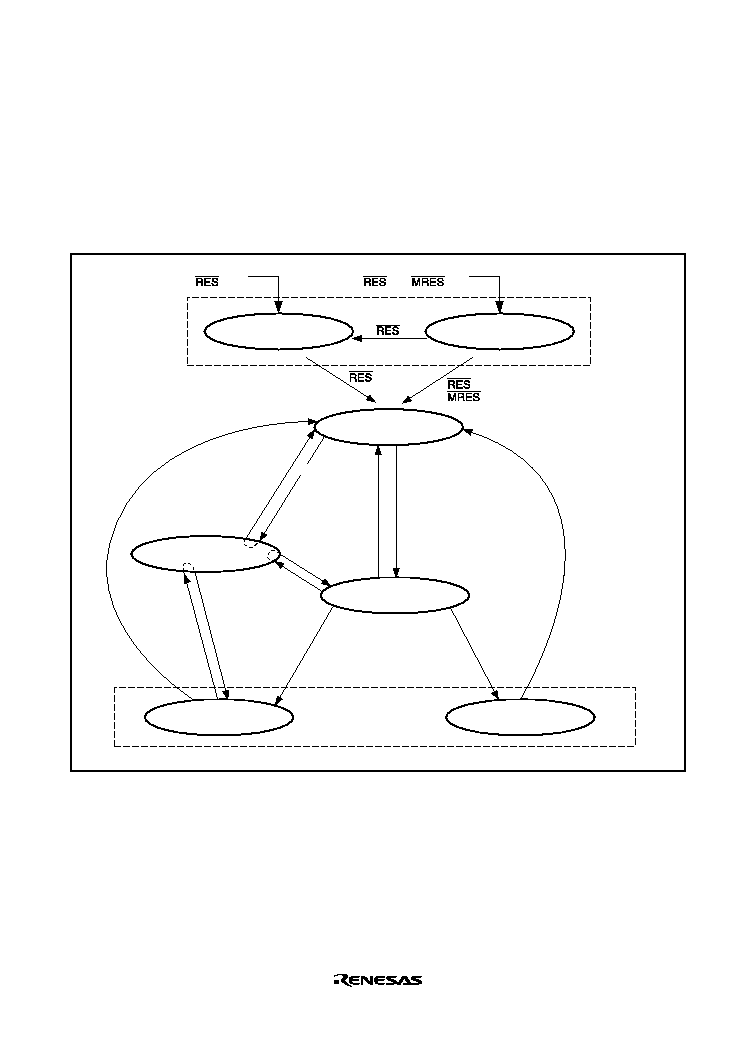
Rev. 2.0, 09/02, page 41 of 732
2.6
Processing States
2.6.1
State Transitions
The CPU has five processing states: reset, exception processing, bus release, program execution
and power-down. Figure 2.4 shows the transitions between the states.
From any state
when
= 0
From any state when
= 1,
= 0,
= 0
Power-on reset state
Manual reset state
Program execution state
Bus release state
Sleep mode
Software standby mode
Exception
processing state
When an internal power-on
reset by WDT or internal
manual reset by
WDT occurs
Exception
processing
source
occurs
Exception
processing
ends
Bus request
generated
Bus request
cleared
SSBY bit set
for SLEEP
instruction
NMI or IRQ interrupt
source occurs
Power-down state
= 1
= 1,
= 1
SSBY bit cleared
for SLEEP
instruction
Reset state
Bus request
cleared
Bus request
cleared
Bus request
generated
Bus request
generated
Figure 2.4 Transitions between Processing States

Rev. 2.0, 09/02, page 42 of 732
Reset State: The CPU resets in the reset state. When the
RES pin level goes low, the power-on
reset state is entered. When the
RES pin is high and the MRES pin is low, the manual reset state is
entered.
Exception Processing State: The exception processing state is a transient state that occurs when
exception processing sources such as resets or interrupts alter the CPU's processing state flow.
For a reset, the initial values of the program counter (PC) (execution start address) and stack
pointer (SP) are fetched from the exception processing vector table and stored; the CPU then
branches to the execution start address and execution of the program begins.
For an interrupt, the stack pointer (SP) is accessed and the program counter (PC) and status
register (SR) are saved to the stack area. The exception service routine start address is fetched
from the exception processing vector table; the CPU then branches to that address and the program
starts executing, thereby entering the program execution state.
Program Execution State: In the program execution state, the CPU sequentially executes the
program.
Power-Down State: In the power-down state, the CPU operation halts and power consumption
declines. The SLEEP instruction places the CPU in the sleep mode or the software standby mode.
Bus Release State: In the bus release state, the CPU releases bus mastership to the device that has
requested them.

Rev. 2.0, 09/02, page 43 of 732
Section 3 MCU Operating Modes
3.1
Selection of Operating Modes
This LSI has four operating modes and four clock modes. The operating mode is determined by
the setting of MD3 to MD0, and FWP pins. Do not change these pins during LSI operation (while
power is on). Do not set these pins in the other way than the combination shown in table 3.1.
When power is applied to the system, be sure to conduct power-on reset.
Table 3.1 Selection of Operating Modes
Pin Setting
Bus Width of
CS0 Area
Mode
No.
FWP MD3
*
1
MD2
*
1
MD1 MD0 Mode Name
On-Chip ROM SH7144 SH7145
Mode 0 1
x
x
0
0
MCU
extension
mode 0
Not Active
8 bits
16 bits
Mode 1 1
x
x
0
1
MCU
extension
mode 1
Not Active
16 bits
32 bits
Mode 2 1
x
x
1
0
MCU
extension
mode 2
Active
Set by BCR1 of
BSC
Mode 3 1
x
x
1
1
Single chip
mode
Active
*
2
0
x
x
0
0
Set by BCR1 of
BSC
*
2
0
x
x
0
1
Boot mode
*
2
Active
*
2
0
x
x
1
0
Set by BCR1 of
BSC
*
2
0
x
x
1
1
User
programming
mode
*
2
Active
--
Notes: The symbol x means "Don't care."
1. MD3 and MD2 pins are used to select clock mode.
2. User programming mode for flash memory. Supported in only F-ZTAT version.
There are two modes as the MCU operating modes: MCU extension mode and single chip mode.
There are two modes to program the flash memory (on-board programming mode): boot mode and
user programming mode.

Rev. 2.0, 09/02, page 44 of 732
The clock mode is selected by the input of MD2 and MD3 pins.
Table 3.2 Clock Mode Setting
Pin Setting
Clock Ratio (when an input clock is 1)
Clock Mode No.
MD3
MD2
System clock (
)
Peripheral
clock (P
)
System clock
output (CK)
0
0
0
◊
1
◊
1
◊
1
1
0
1
◊
2
◊
2
◊
2
2
1
0
◊
4
◊
4
*
◊
4
3
1
1
◊
4
◊
2
◊
4
Note:
*
The maximum clock input frequency is 10MHz because the p
is specified as 40MHz or
less.
3.2
Input/Output Pin
Table 3.3 describes the configuration of operating mode related pin.
Table 3.3 Operating Mode Pin Configuration
Pin Name
Input/Output
Function
MD0
Input
Designates operating mode through the level applied to this pin
MD1
Input
Designates operating mode through the level applied to this pin
MD2
Input
Designates clock mode through the level applied to this pin
MD3
Input
Designates clock mode through the level applied to this pin
FWP
Input
Pin for the hardware protection against programming/erasing the
on-chip flash memory

Rev. 2.0, 09/02, page 45 of 732
3.3
Explanation of Operating Modes
3.3.1
Mode 0 (MCU extension mode 0)
CS0 area becomes an external memory space with 8-bit bus width in SH7144 or 16-bit bus width
in SH7145.
3.3.2
Mode 1 (MCU extension mode 1)
CS0 area becomes an external memory space with 16-bit bus width in SH7144 or 32-bit bus width
in SH7145.
3.3.3
Mode 2 (MCU extension mode 2)
The on-chip ROM is active and CS0 area can be used in this mode.
3.3.4
Mode 3 (Single chip mode)
All ports can be used in this mode, however the external address cannot be used.
3.3.5
Clock mode
The input waveform frequency can be used as is, doubled or quadrupled as system clock
frequency in mode 0 to mode 3.
Rev. 2.0, 09/02, page 46 of 732
3.4
Address Map
The address map for the operating modes are shown in figure 3.1.
H'00000000
H'FFFF7FFF
H'FFFF8000
H'003FFFFF
H'007FFFFF
H'00400000
H'00800000
H'00BFFFFF
H'00C00000
H'00FFFFFF
H'01000000
H'FFFFBFFF
H'FFFFC000
Modes 0 and 1
On-chip ROM disabled mode
Modes 2
On-chip ROM enabled mode
Modes 3
Single-chip mode
On-chip RAM(8kB)
On-chip RAM(8kB)
On-chip RAM(8kB)
(256kB)
(256kB)
H'FFFFFFFF
H'FFFFDFFF
H'FFFFE000
H'00000000
H'00200000
H'FFFF7FFF
H'FFFF8000
H'003FFFFF
H'0003FFFF
H'007FFFFF
H'00400000
H'00040000
H'00040000
H'00800000
H'00BFFFFF
H'00C00000
H'00FFFFFF
H'01000000
H'FFFFBFFF
H'FFFFC000
H'FFFFFFFF
H'FFFFDFFF
H'FFFFE000
H'FFFF7FFF
H'FFFF8000
H'FFFFBFFF
H'FFFFC000
H'FFFFFFFF
H'FFFFDFFF
H'FFFFE000
H'00000000
H'0003FFFF
On-chip ROM
Reserved area
Reserved area
Reserved area
CS0 area
CS1 area
CS2 area
CS3 area
CS1 area
CS2 area
CS3 area
CS0 area
Reserved area
Reserved area
On-chip peripheral
I/O registers
On-chip peripheral
I/O registers
On-chip peripheral
I/O registers
Reserved area
Reserved area
On-chip ROM
Figure 3.1 The Address Map for Each Operating Mode
3.5
Initial State in This LSI
In the initial state of this LSI, some of on-chip modules are set in module standby state for saving
power.
When operating these modules, clear module standby state according to the procedure in section
24, Power-Down Modes.
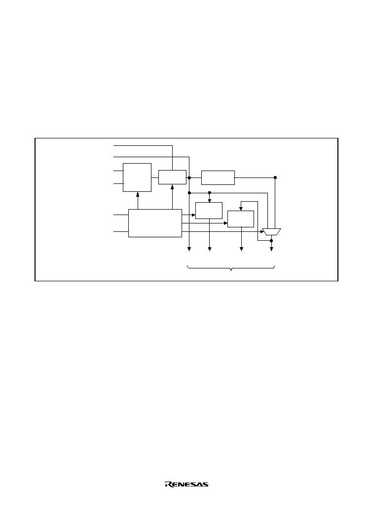
CPG0111A_010020020700
Rev. 2.0, 09/02, page 47 of 732
Section 4 Clock Pulse Generator
This LSI has an on-chip clock pulse generator (CPG) that generates the system clock (
)and the
peripheral clock(P
), and then makes internal clock (
/2 to
/8192 and P
/2 to P
/1024) out of
this generated clock. The CPG consists of an oscillator, PLL circuit, and pre-scaler. A block
diagram of the clock pulse generator is shown in figure 4.1. The frequency from the oscillator can
be modified by the PLL circuit.
PLLCAP
EXTAL
XTAL
MD2
MD3
Pre-scaler
Pre-scaler
Oscillator
for internal circuit
PLL circuit
Clock divider
(
◊
1/2)
Clock mode
control circuitry
/2 to
/8192
P
/2 to
P
/1024
CK
P
Figure 4.1 Block Diagram of the Clock Pulse Generator

Rev. 2.0, 09/02, page 48 of 732
Table 4.1 shows the operating clock for each module.
Table 4.1 Operating clock for each module
Operating clock
Operating Module
System clock (
)
CPU
UBC
DTC
BSC
DMAC
WDT
AUD
ROM
RAM
Peripheral clock (P
)
MTU
POE
SCI
I
2
C
A/D
CMT
H-UDI
4.1
Oscillator
Clock pulses can be supplied from a connected crystal resonator or an external clock.
4.1.1
Connecting a Crystal Oscillator
Circuit Configuration: A crystal oscillator can be connected as shown in figure 4.2. Use the
damping resistance (Rd) listed in table 4.2. Use an AT-cut parallel-resonance type crystal
oscillator that has a resonance frequency of 4 to 12.5 MHz. It is recommended to consult crystal
dealer concerning the compatibility of the crystal oscillator and the LSI.
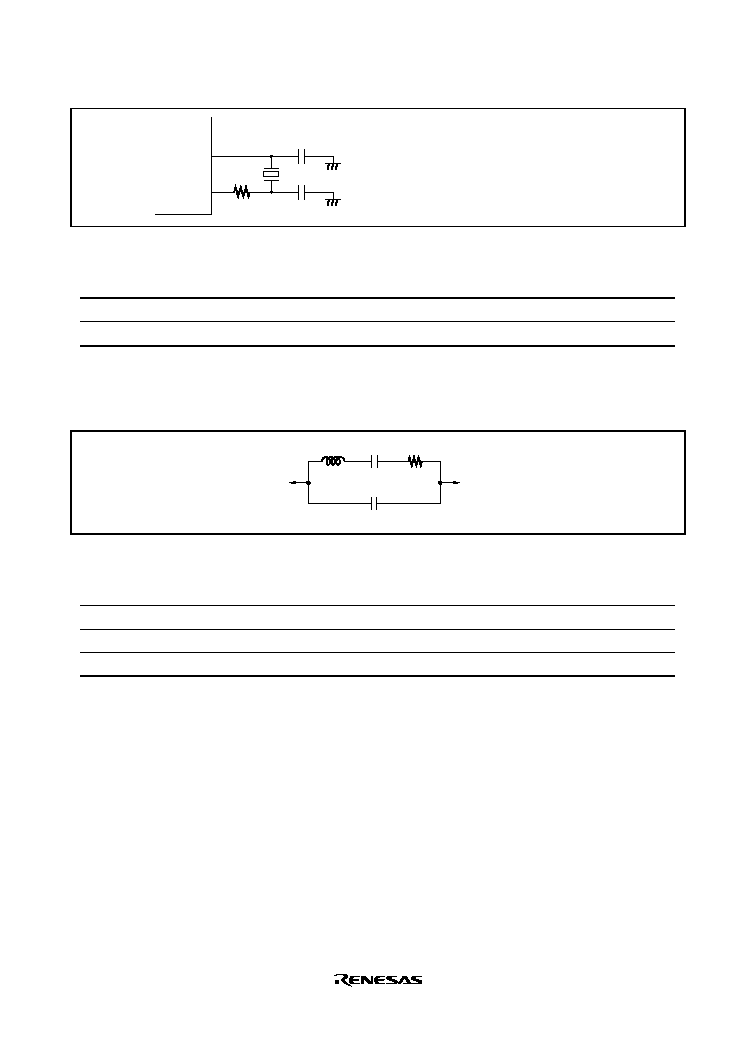
Rev. 2.0, 09/02, page 49 of 732
EXTAL
XTAL
R
d
C
L2
C
L1
C
L1
= C
L2
= 18≠22 pF (Recommended value)
Figure 4.2 Connection of the Crystal Oscillator (Example)
Table 4.2 Damping Resistance Values
Frequency (MHz)
4
8
10
12.5
Rd (
)
500
200
0
0
Crystal Resonator: Figure 4.3 shows an equivalent circuit of the crystal resonator. Use a crystal
resonator with the characteristics listed in table 4.3.
XTAL
C
L
EXTAL
C
0
L
Rs
Figure 4.3 Crystal Resonator Equivalent Circuit
Table 4.3 Crystal Resonator Characteristics
Frequency (MHz)
4
8
10
12.5
Rs max (
)
120
80
60
50
C
0
max (pF)
7
7
7
7
4.1.2
External Clock Input Method
Figure 4.4 shows an example of an external clock input connection. In this case, make the external
clock high level to stop it when in software standby mode. During operation, make the external
input clock frequency 4 to 12.5 MHz.
When leaving the XTAL pin open, make sure the parasitic capacitance is less than 10 pF.
Even when inputting an external clock, be sure to wait at least the oscillation stabilization time in
power-on sequence or in releasing software standby mode, in order to ensure the PLL stabilization
time.

Rev. 2.0, 09/02, page 50 of 732
EXTAL
XTAL
External clock input
Open state
Figure 4.4 Example of External Clock Connection
4.2
Function for Detecting the Oscillator Halt
This CPG can detect a clock halt and automatically cause the timer pins to become high-
impedance when any system abnormality causes the oscillator to halt. That is, when a change of
EXTAL has not been detected, the high-current 6 pins (PE9/TIOC3B/SCK3/
TRST*,
PE11/TIOC3D/RXD3/TDO*, PE12/TIOC4A/TXD3/TCK*, PE13/TIOC4B/
MRES,
PE14/TIOC4C/DACK0, PE15/TIOC4D/DACK1/
IRQOUT) can be set to high-impedance
regardless of PFC setting. Refer to section 17.1.11, High-Current Port Control Register (PPCR),
for more details.
Even in software standby mode, these 6 pins can be set to high-impedance regardless of PFC
setting. Refer to section 17.1.11, High-Current Port Control Register (PPCR), for more details.
These pins enter the normal state after software standby mode is released. When abnormalities that
halt the oscillator occur except in software standby mode, other LSI operations become undefined.
In this case, LSI operations, including these 6 pins, become undefined even when the oscillator
operation starts again.
In the case of using E10A, the high-impedance function is disabled when an oscillation stop is
detected, or when in software standby state for the three pins of PE9/TIOC3B/SCK3/
TRST,
PE11/TIOC3D/RXD3/TDO, and PE12/TIOC4A/TxD3/TCK of the SH7145.
Note: * Only in the SH7145.
4.3
Usage Notes
4.3.1
Note on Crystal Resonator
A sufficient evaluation at the user's site is necessary to use the LSI, by referring the resonator
connection examples shown in this section, because various characteristics related to the crystal
resonator are closely linked to the user's board design. As the oscillator circuit's circuit constant
will depend on the resonator and the floating capacitance of the mounting circuit, the value of each
external circuit's component should be determined in consultation with the resonator
manufacturer. The design must ensure that a voltage exceeding the maximum rating is not applied
to the oscillator pin.
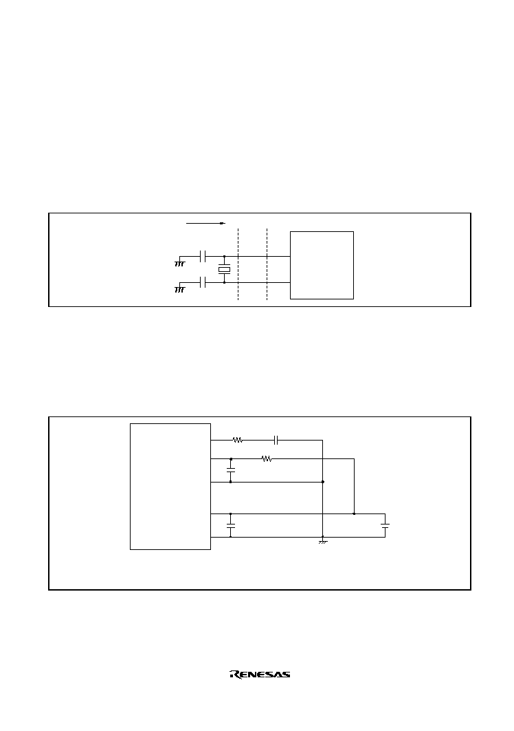
Rev. 2.0, 09/02, page 51 of 732
4.3.2
Notes on Board Design
Measures against radiation noise are taken in this LSI. If further reduction in radiation noise is
needed, it is recommended to use a multiple layer board and provide a layer exclusive to the
system ground.
When using a crystal oscillator, place the crystal oscillator and its load capacitors as close as
possible to the XTAL and EXTAL pins. Do not route any signal lines near the oscillator circuitry
as shown in figure 4.5. Otherwise, correct oscillation can be interfered by induction.
C
L2
Signal A Signal B
This LSI
C
L1
XTAL
EXTAL
Avoid
Figure 4.5 Cautions for Oscillator Circuit System Board Design
A circuitry shown in figure 4.6 is recommended as an external circuitry around the PLL. Place
oscillation stabilization capacitor C1 close to the PLLCAP pin, and ensure that no other signal
lines cross this line. Separate the PLL power lines (PLLVcc, PLLVss) and the system power lines
(Vcc, Vss) at the board power supply source, and be sure to insert bypass capacitors CB and CPB
close to the pins.
PLLCAP
PLLV
CC
PLLV
SS
V
CC
V
SS
C1: 470 pF
CPB = 0.1
µ
F
*
CB = 0.1
µ
F
*
(Values are preliminary recommended values.)
Note:
*
CB and CPB are laminated ceramic type.
Rp=200
R1=3k
Figure 4.6 Recommended External Circuitry around the PLL
In principle, electromagnetic waves are emitted from an LSI in operation. This LSI regards the
lower of the system clock (
) and the peripheral clock (P
) as fundamental (for example, if
= 40

Rev. 2.0, 09/02, page 52 of 732
MHz and P
= 40 MHz, then 40 MHz), and the peak of electromagnetic waves is in the high
frequency band. When this LSI is used adjacent to apparatuses sensible to electromagnetic waves
such as FM/VHF band receivers, it is recommended to use a board with at least four layers and
provide a layer exclusive to the system ground.

Rev. 2.0, 09/02, page 53 of 732
Section 5 Exception Processing
5.1
Overview
5.1.1
Types of Exception Processing and Priority
Exception processing is started by four sources: resets, address errors, interrupts and instructions
and have the priority, as shown in table 5.1. When several exception processing sources occur at
once, they are processed according to the priority.
Table 5.1 Types of Exception Processing and Priority Order
Exception Source
Priority
Reset
Power-on reset
High
Manual reset
CPU address error or AUD address error
*
1
Address
error
DMAC/DTC address error
Interrupt
NMI
User break
H-UDI
IRQ
On-chip
peripheral
modules:
∑
Direct memory access controller (DMAC)
∑
Multifunction timer unit (MTU)
∑
Serial communication interface 0 and 1(SCI0 and SCI1)
∑
A/D converter 0 and 1 (A/D0, A/D1)
∑
Data transfer controller (DTC)
∑
Compare match timer 0 and 1 (CMT0, CMT1)
∑
Watchdog timer (WDT)
∑
Input/output port (I/O) (MTU)
∑
Serial communication interface 2 and 3 (SCI2 and SCI3)
∑
IIC bus interface (IIC)
Instructions Trap instruction (TRAPA instruction)
General illegal instructions (undefined code)
Illegal slot instructions (undefined code placed directly after a delay
branch instruction
*
2
or instructions that rewrite the PC
*
3
)
Low
Notes:
1. Only in the F-ZTAT version.
2. Delayed branch instructions: JMP, JSR, BRA, BSR, RTS, RTE, BF/S, BT/S, BSRF, and
BRAF.
3. Instructions that rewrite the PC: JMP, JSR, BRA, BSR, RTS, RTE, BT, BF, TRAPA,
BF/S, BT/S, BSRF, and BRAF.

Rev. 2.0, 09/02, page 54 of 732
5.1.2
Exception Processing Operations
The exception processing sources are detected and begin processing according to the timing
shown in table 5.2.
Table 5.2 Timing for Exception Source Detection and Start of Exception Processing
Exception
Source
Timing of Source Detection and Start of Processing
Power-on reset
Starts when the
RES
pin changes from low to high or when
WDT overflows.
Reset
Manual reset
Starts when the
MRES
pin changes from low to high.
Address error
Interrupts
Detected when instruction is decoded and starts when the
execution of the previous instruction is completed.
Trap instruction
Starts from the execution of a TRAPA instruction.
General illegal
instructions
Starts from the decoding of undefined code anytime except
after a delayed branch instruction (delay slot).
Instructions
Illegal slot
instructions
Starts from the decoding of undefined code placed in a delayed
branch instruction (delay slot) or of instructions that rewrite the
PC.
When exception processing starts, the CPU operates as follows:
1. Exception processing triggered by reset:
The initial values of the program counter (PC) and stack pointer (SP) are fetched from the
exception processing vector table (PC and SP are respectively the H'00000000 and
H'00000004 addresses for power-on resets and the H'00000008 and H'0000000C addresses for
manual resets). See section 5.1.3, Exception Processing Vector Table, for more information.
H'00000000 is then written to the vector base register (VBR) , and H'F (B'1111) is written to
the interrupt mask bits (I3 to I0) of the status register (SR). The program begins running from
the PC address fetched from the exception processing vector table.
2. Exception processing triggered by address errors, interrupts and instructions:
SR and PC are saved to the stack indicated by R15. For interrupt exception processing, the
interrupt priority level is written to the SR's interrupt mask bits (I3 to I0). For address error
and instruction exception processing, the I3 to I0 bits are not affected. The start address is then
fetched from the exception processing vector table and the program begins running from that
address.

Rev. 2.0, 09/02, page 55 of 732
5.1.3
Exception Processing Vector Table
Before exception processing begins running, the exception processing vector table must be set in
memory. The exception processing vector table stores the start addresses of exception service
routines. (The reset exception processing table holds the initial values of PC and SP.)
All exception sources are given different vector numbers and vector table address offsets. The
vector table addresses are calculated from these vector numbers and vector table address offsets.
During exception processing, the start addresses of the exception service routines are fetched from
the exception processing vector table that is indicated by this vector table address.
Table 5.3 shows the vector numbers and vector table address offsets. Table 5.4 shows how vector
table addresses are calculated.
Table 5.3 Exception Processing Vector Table
Exception Sources
Vector Numbers
Vector Table Address Offset
Power-on reset
PC
0
H'00000000 to H'00000003
SP
1
H'00000004 to H'00000007
Manual reset
PC
2
H'00000008 to H'0000000B
SP
3
H'0000000C to H'0000000F
General illegal instruction
4
H'00000010 to H'00000013
(Reserved by system)
5
H'00000014 to H'00000017
Slot illegal instruction
6
H'00000018 to H'0000001B
(Reserved by system)
7
H'0000001C to H'0000001F
8
H'00000020 to H'00000023
CPU address error or AUD address error
*
1
9
H'00000024 to H'00000027
DMAC/DTC address error
10
H'00000028 to H'0000002B
Interrupts
NMI
11
H'0000002C to H'0000002F
User break
12
H'00000030 to H'00000033
(Reserved by system)
13
H'00000034 to H'00000037
H-UDI
14
H'00000038 to H'0000003B
(Reserved by system)
15
:
31
H'0000003C to H'0000003F
:
H'0000007C to H'0000007F
Trap instruction (user vector)
32
:
63
H'00000080 to H'00000083
:
H'000000FC to H'000000FF

Rev. 2.0, 09/02, page 56 of 732
Exception Sources
Vector Numbers
Vector Table Address Offset
Interrupts
IRQ0
64
H'00000100 to H'00000103
IRQ1
65
H'00000104 to H'00000107
IRQ2
66
H'00000108 to H'0000010B
IRQ3
67
H'0000010C to H'0000010F
IRQ4
68
H'00000110 to H'00000113
IRQ5
69
H'00000114 to H'00000117
IRQ6
70
H'00000118 to H'0000011B
IRQ7
71
H'0000011C to H'0000011F
On-chip peripheral module
*
2
72
:
255
H'00000120 to H'00000124
:
H'000003FC to H'000003FF
Note: 1. Only in the F-ZTAT version.
2. The vector numbers and vector table address offsets for each on-chip peripheral
module interrupt are given in section 6, Interrupt Controller (INTC), and table 6.2,
Interrupt Exception Processing Vectors and Priorities.
Table 5.4 Calculating Exception Processing Vector Table Addresses
Exception Source
Vector Table Address Calculation
Resets
Vector table address = (vector table address offset)
= (vector number)
◊
4
Address errors, interrupts,
instructions
Vector table address = VBR + (vector table address offset)
= VBR + (vector number)
◊
4
Notes: 1. VBR: Vector base register
2. Vector table address offset: See table 5.3.
3. Vector number: See table 5.3.

Rev. 2.0, 09/02, page 57 of 732
5.2
Resets
5.2.1
Types of Reset
Resets have the highest priority of any exception source. There are two types of resets: manual
resets and power-on resets. As table 5.5 shows, both types of resets initialize the internal status of
the CPU. In power-on resets, all registers of the on-chip peripheral modules are initialized; in
manual resets, they are not.
Table 5.5 Reset Status
Conditions for Transition
to Reset Status
Internal Status
Type
RES
RES
RES
RES
WDT
Overflow
MRES
MRES
MRES
MRES
CPU/INTC
On-Chip
Peripheral
Module
PFC, IO Port
Low
--
--
Initialized
Initialized
Initialized
Power-on reset
High
Overflow
High
Initialized
Initialized
Not initialized
Manual reset
High
--
Low
Initialized
Not initialized Not initialized
5.2.2
Power-On Reset
Power-On Reset by
RES
RES
RES
RES Pin: When the RES pin is driven low, the LSI becomes to be a power-
on reset state. To reliably reset the LSI, the
RES pin should be kept at low for at least the duration
of the oscillation settling time when applying power or when in software standby mode (when the
clock circuit is halted) or at least 20 t
cyc
when the clock circuit is running. During power-on reset,
CPU internal status and all registers of on-chip peripheral modules are initialized. See Appendix
A, Pin States, for the status of individual pins during the power-on reset status.
In the power-on reset status, power-on reset exception processing starts when the
RES pin is first
driven low for a set period of time and then returned to high. The CPU will then operate as
follows:
1. The initial value (execution start address) of the program counter (PC) is fetched from the
exception processing vector table.
2. The initial value of the stack pointer (SP) is fetched from the exception processing vector table.
3. The vector base register (VBR) is cleared to H'00000000 and the interrupt mask bits (I3 to I0)
of the status register (SR) are set to H'F (B'1111).
4. The values fetched from the exception processing vector table are set in PC and SP, then the
program begins executing.
Be certain to always perform power-on reset processing when turning the system power on.

Rev. 2.0, 09/02, page 58 of 732
Power-On Reset by WDT: When a setting is made for a power-on reset to be generated in the
WDT's watchdog timer mode, and the WDT's TCNT overflows, the LSI becomes to be a power-
on reset state.
The pin function controller (PFC) registers and I/O port registers are not initialized by the reset
signal generated by the WDT (these registers are only initialized by a power-on reset from outside
of the chip).
If reset caused by the input signal at the
RES pin and a reset caused by WDT overflow occur
simultaneously, the
RES pin reset has priority, and the WOVF bit in RSTCSR is cleared to 0.
When WDT-initiated power-on reset processing is started, the CPU operates as follows:
1. The initial value (execution start address) of the program counter (PC) is fetched from the
exception processing vector table.
2. The initial value of the stack pointer (SP) is fetched from the exception processing vector table.
3. The vector base register (VBR) is cleared to H'00000000 and the interrupt mask bits (I3-I0) of
the status register (SR) are set to H'F (B'1111).
4. The values fetched from the exception processing vector table are set in the PC and SP, then
the program begins executing.
5.2.3
Manual Reset
When the
RES pin is high and the MRES pin is driven low, the LSI becomes to be a manual reset
state. To reliably reset the LSI, the
MRES pin should be kept at low for at least the duration of the
oscillation settling time that is set in WDT when in software standby mode (when the clock is
halted) or at least 20 t
cyc
when the clock is operating. During manual reset, the CPU internal status
is initialized. Registers of on-chip peripheral modules are not initialized. When the LSI enters
manual reset status in the middle of a bus cycle, manual reset exception processing does not start
until the bus cycle has ended. Thus, manual resets do not abort bus cycles. However, once
MRES
is driven low, hold the low level until the CPU becomes to be a manual reset mode after the bus
cycle ends. (Keep at low level for at least the longest bus cycle). See Appendix A, Pin States, for
the status of individual pins during manual reset mode.
In the manual reset status, manual reset exception processing starts when the
MRES pin is first
kept low for a set period of time and then returned to high. The CPU will then operate in the same
procedures as described for power-on resets.

Rev. 2.0, 09/02, page 59 of 732
5.3
Address Errors
5.3.1
The Cause of Address Error Exception
Address errors occur when instructions are fetched or data read or written, as shown in table 5.6.
Table 5.6 Bus Cycles and Address Errors
Bus Cycle
Type
Bus Master
Bus Cycle Description
Address Errors
CPU
Instruction fetched from even address
None (normal)
Instruction fetched from odd address
Address error occurs
Instruction fetched from other than on-chip
peripheral module space
*
None (normal)
Instruction fetched from on-chip peripheral
module space
*
Address error occurs
Instruction
fetch
Instruction fetched from external memory
space when in single chip mode
Address error occurs
Word data accessed from even address
None (normal)
Word data accessed from odd address
Address error occurs
Longword data accessed from a longword
boundary
None (normal)
Longword data accessed from other than a
long-word boundary
Address error occurs
Byte or word data accessed in on-chip
peripheral module space
*
None (normal)
Longword data accessed in 16-bit on-chip
peripheral module space
*
None (normal)
Longword data accessed in 8-bit on-chip
peripheral module space
*
Address error occurs
Data
read/write
CPU or
DMAC or
AUD or DTC
External memory space accessed when in
single chip mode
Address error occurs
Note:
*
See section 9, Bus State Controller (BSC), for more information on the on-chip peripheral
module space.

Rev. 2.0, 09/02, page 60 of 732
5.3.2
Address Error Exception Processing
When an address error occurs, the bus cycle in which the address error occurred ends, the current
instruction finishes, and then address error exception processing starts. The CPU operates as
follows:
1. The status register (SR) is saved to the stack.
2. The program counter (PC) is saved to the stack. The PC value saved is the start address of the
instruction to be executed after the last executed instruction.
3. The start address of the exception service routine is fetched from the exception processing
vector table that corresponds to the occurred address error, and the program starts executing
from that address. The jump in this case is not a delayed branch.
5.4
Interrupts
5.4.1
Interrupt Sources
Table 5.7 shows the sources that start the interrupt exception processing. They are NMI, user
breaks, H-UDI, IRQ and on-chip peripheral modules.
Table 5.7 Interrupt Sources
Type
Request Source
Number of Sources
NMI
NMI pin (external input)
1
User break
User break controller (UBC)
1
H-UDI
Hitachi user debug interface (H-UDI)
1
IRQ
IRQ0
to
IRQ7
pins (external input)
8
On-chip peripheral module
Direct Memory Access Controller
(DMAC)
4
Multifunction timer unit (MTU)
23
Data transfer controller (DTC)
1
Compare match timer (CMT)
2
A/D converter (A/D0 and A/D1)
2
Serial communication interface
(SCI0
-
SCI3)
16
Watchdog timer (WDT)
1
Input/output Port
1
IIC bus interface (IIC)
1

Rev. 2.0, 09/02, page 61 of 732
Each interrupt source is allocated a different vector number and vector table offset. See section 6,
Interrupt Controller (INTC), and table 6.2, Interrupt Exception Processing Vectors and Priorities,
for more information on vector numbers and vector table address offsets.
5.4.2
Interrupt Priority Level
The interrupt priority order is predetermined. When multiple interrupts occur simultaneously
(overlapped interruptions), the interrupt controller (INTC) determines their relative priorities and
starts the exception processing according to the results.
The priority order of interrupts is expressed as priority levels 0 to 16, with priority 0 the lowest
and priority 16 the highest. The NMI interrupt has priority 16 and cannot be masked, so it is
always accepted. The priority level of user break interrupt and H-UDI is 15. IRQ interrupts and
on-chip peripheral module interrupt priority levels can be set freely using the INTC's interrupt
priority level setting registers A through J (IPRA to IPRJ) as shown in table 5.8. The priority
levels that can be set are 0 to 15. Level 16 cannot be set. See section 6.3.4, Interrupt Priority
Registers A to J (IPRA to IPRJ), for more information on IPRA to IPRJ.
Table 5.8 Interrupt Priority Order
Type
Priority Level
Comment
NMI
16
Fixed priority level. Cannot be masked.
User break
15
Fixed priority level.
H-UDI
15
Fixed priority level.
IRQ
On-chip peripheral module
0 to 15
Set with interrupt priority level setting registers
A through J (IPRA to IPRJ).
5.4.3
Interrupt Exception Processing
When an interrupt occurs, the interrupt controller (INTC) ascertains its priority level. NMI is
always accepted, but other interrupts are only accepted if they have a priority level higher than the
priority level set in the interrupt mask bits (I3 to I0) of the status register (SR).
When an interrupt is accepted, exception processing begins. In interrupt exception processing, the
CPU saves SR and the program counter (PC) to the stack. The priority level value of the accepted
interrupt is written to SR bits I3 to I0. For NMI, however, the priority level is 16, but the value set
in I3 to I0 is H'F (level 15). Next, the start address of the exception service routine is fetched from
the exception processing vector table for the accepted interrupt, that address is jumped to and
execution begins. See section 6.6, Interrupt Operation, for more information on the interrupt
exception processing.

Rev. 2.0, 09/02, page 62 of 732
5.5
Exceptions Triggered by Instructions
5.5.1
Types of Exceptions Triggered by Instructions
Exception processing can be triggered by trap instruction, illegal slot instructions, and general
illegal instructions, as shown in table 5.9.
Table 5.9 Types of Exceptions Triggered by Instructions
Type
Source Instruction
Comment
Trap instruction
TRAPA
--
Illegal slot
instructions
Undefined code placed
immediately after a delayed
branch instruction (delay slot) or
instructions that rewrite the PC
Delayed branch instructions: JMP, JSR,
BRA, BSR, RTS, RTE, BF/S, BT/S, BSRF,
BRAF
Instructions that rewrite the PC: JMP, JSR,
BRA, BSR, RTS, RTE, BT, BF, TRAPA,
BF/S, BT/S, BSRF, BRAF
General illegal
instructions
Undefined code anywhere
besides in a delay slot
--
5.5.2
Trap Instructions
When a TRAPA instruction is executed, trap instruction exception processing starts. The CPU
operates as follows:
1. The status register (SR) is saved to the stack.
2. The program counter (PC) is saved to the stack. The PC value saved is the start address of the
instruction to be executed after the TRAPA instruction.
3. The start address of the exception service routine is fetched from the exception processing
vector table that corresponds to the vector number specified in the TRAPA instruction. That
address is jumped to and the program starts executing. The jump in this case is not a delayed
branch.

Rev. 2.0, 09/02, page 63 of 732
5.5.3
Illegal Slot Instructions
An instruction placed immediately after a delayed branch instruction is called "instruction placed
in a delay slot". When the instruction placed in the delay slot is an undefined code, illegal slot
exception processing starts after the undefined code is decoded. Illegal slot exception processing
also starts when an instruction that rewrites the program counter (PC) is placed in a delay slot and
the instruction is decoded. The CPU handles an illegal slot instruction as follows:
1. The status register (SR) is saved to the stack.
2. The program counter (PC) is saved to the stack. The PC value saved is the target address of the
delayed branch instruction immediately before the undefined code or the instruction that
rewrites the PC.
3. The start address of the exception service routine is fetched from the exception processing
vector table that corresponds to the exception that occurred. That address is jumped to and the
program starts executing. The jump in this case is not a delayed branch.
5.5.4
General Illegal Instructions
When undefined code placed anywhere other than immediately after a delayed branch instruction
(i.e., in a delay slot) is decoded, general illegal instruction exception processing starts. The CPU
handles the general illegal instructions in the same procedures as in the illegal slot instructions.
Unlike processing of illegal slot instructions, however, the program counter value that is stacked is
the start address of the undefined code.
5.6
Cases when Exception Sources Are Not Accepted
When an address error or interrupt is generated directly after a delayed branch instruction or
interrupt-disabled instruction, it is sometimes not accepted immediately but stored instead, as
shown in table 5.10. In this case, it will be accepted when an instruction that can accept the
exception is decoded.
Table 5.10 Generation of Exception Sources Immediately after a Delayed Branch
Instruction or Interrupt-Disabled Instruction
Exception Source
Point of Occurrence
Address Error
Interrupt
Immediately after a delayed branch instruction
*
1
Not accepted
Not accepted
Immediately after an interrupt-disabled instruction
*
2
Accepted
Not accepted
Notes: 1. Delayed branch instructions: JMP, JSR, BRA, BSR, RTS, RTE, BF/S, BT/S, BSRF, and
BRAF
2. Interrupt-disabled instructions: LDC, LDC.L, STC, STC.L, LDS, LDS.L, STS, and STS.L

Rev. 2.0, 09/02, page 64 of 732
5.6.1
Immediately after a Delayed Branch Instruction
When an instruction placed immediately after a delayed branch instruction (delay slot) is decoded,
neither address errors nor interrupts are accepted. The delayed branch instruction and the
instruction placed immediately after it (delay slot) are always executed consecutively, so no
exception processing occurs during this period.
5.6.2
Immediately after an Interrupt-Disabled Instruction
When an instruction placed immediately after an interrupt-disabled instruction is decoded,
interrupts are not accepted. Address errors can be accepted.
Rev. 2.0, 09/02, page 65 of 732
5.7
Stack Status after Exception Processing Ends
The status of the stack after exception processing ends is shown in table 5.11.
Table 5.11 Stack Status after Exception Processing Ends
Types
Stack Status
Address error
32 bits
32 bits
SR
Address of instruction
after executed instruction
SP
Trap instruction
32 bits
32 bits
SR
Address of instruction
after TRAPA instruction
SP
General illegal instruction
32 bits
32 bits
SR
Address of instruction after
general illegal instruction
SP
Interrupt
32 bits
32 bits
SR
Address of instruction
after executed instruction
SP
Illegal slot instruction
32 bits
32 bits
SR
Jump destination address
of delay branch instruction
SP

Rev. 2.0, 09/02, page 66 of 732
5.8
Usage Notes
5.8.1
Value of Stack Pointer (SP)
The value of the stack pointer must always be a multiple of four. If it is not, an address error will
occur when the stack is accessed during exception processing.
5.8.2
Value of Vector Base Register (VBR)
The value of the vector base register must always be a multiple of four. If it is not, an address error
will occur when the stack is accessed during exception processing.
5.8.3
Address Errors Caused by Stacking of Address Error Exception Processing
When the value of the stack pointer is not a multiple of four, an address error will occur during
stacking of the exception processing (interrupts, etc.) and address error exception processing will
start after the first exception processing is ended. Address errors will also occur in the stacking for
this address error exception processing. To ensure that address error exception processing does not
go into an endless loop, no address errors are accepted at that point. This allows program control
to be shifted to the service routine for address error exception and enables error processing.
When an address error occurs during exception processing stacking, the stacking bus cycle (write)
is executed. During stacking of the status register (SR) and program counter (PC), the value of SP
is reduced by 4 for both of SR and PC, therefore the value of SP is still not a multiple of four after
the stacking. The address value output during stacking is the SP value, so the address itself where
the error occurred is output. This means that the write data stacked is undefined.

Rev. 2.0, 09/02, page 67 of 732
Section 6 Interrupt Controller (INTC)
The interrupt controller (INTC) ascertains the priority of interrupt sources and controls interrupt
requests to the CPU.
6.1
Features
∑
16 levels of interrupt priority
∑
NMI noise canceler function
∑
Occurrence of interrupt can be reported externally (
IRQOUT pin)
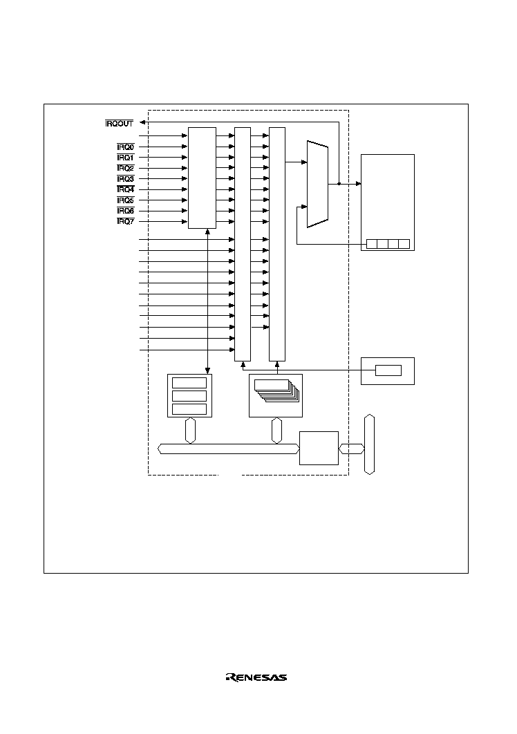
Rev. 2.0, 09/02, page 68 of 732
Figure 6.1 shows a block diagram of the INTC.
NMI
UBC
DMAC
H-UDI
DTC
MTU
CMT
A/D
SCI
WDT
IIC
I/O
(Interrupt request)
(Interrupt request)
(Interrupt request)
(Interrupt request)
(Interrupt request)
(Interrupt request)
(Interrupt request)
(Interrupt request)
(Interrupt request)
(Interrupt request)
(Interrupt request)
Input
control
Com-
parator
Interrupt
request
SR
CPU
I3 I2 I1 I0
Internal bus
Bus
interface
IPRA to IPRJ
ICR1
ISR
ICR2
Module bus
INTC
SCI:
Serial communication interface
WDT: Watchdog
timer
IIC:
IIC bus interface
I/O:
I/O port (port output control unit)
ICR1, ICR2:
Interrupt control register
ISR:
IRQ status register
IPRA to IPRJ: Interrupt priority registers A to J
SR: Status
register
IPR
DTER
DTC
UBC: User break controller
DMAC: Direct memory access controller
H-UDI: Hitachi user debug interface
DTC:
Data transfer controller
MTU: Multifunction timer unit
CMT: Compare match timer
A/D:
A/D converter
CPU/DTC request determination
Priority determination
Figure 6.1 INTC Block Diagram

Rev. 2.0, 09/02, page 69 of 732
6.2
Input/Output Pins
Table 6.1 shows the INTC pin configuration.
Table 6.1 Pin Configuration
Name
Abbreviation
I/O
Function
Non-maskable interrupt input pin
NMI
I
Input of non-maskable interrupt
request signal
Interrupt request input pins
IRQ0
to
IRQ7
I
Input of maskable interrupt request
signals
Interrupt request output pin
IRQOUT
O
Output of notification signal when an
interrupt has occurred
6.3
Register Descriptions
The interrupt controller has the following registers. For details on register addresses and register
states during each processing, refer to section 25, List of Registers.
∑
Interrupt control register 1 (ICR1)
∑
Interrupt control register 2 (ICR2)
∑
IRQ status register (ISR)
∑
Interrupt priority register A (IPRA)
∑
Interrupt priority register B (IPRB)
∑
Interrupt priority register C (IPRC)
∑
Interrupt priority register D (IPRD)
∑
Interrupt priority register E (IPRE)
∑
Interrupt priority register F (IPRF)
∑
Interrupt priority register G (IPRG)
∑
Interrupt priority register H (IPRH)
∑
Interrupt priority register I (IPRI)
∑
Interrupt priority register J (IPRJ)

Rev. 2.0, 09/02, page 70 of 732
6.3.1
Interrupt Control Register 1 (ICR1)
ICR1 is a 16-bit register that sets the input signal detection mode of the external interrupt input
pins NMI and
IRQ0 to IRQ7 and indicates the input signal level at the NMI pin.
Bit
Bit Name Initial Value
R/W
Description
15
NMIL
1/0
R
NMI Input Level
Sets the level of the signal input to the NMI pin. This
bit can be read to determine the NMI pin level. This
bit cannot be modified.
0: NMI input level is low
1: NMI input level is high
14 to 9
--
All 0
R
Reserved bits
These bits are always read as 0. The write value
should always be 0.
8
NMIE
0
R/W
NMI Edge Select
0: Interrupt request is detected on falling edge of NMI
input
1: Interrupt request is detected on rising edge of NMI
input
7
IRQ0S
0
R/W
IRQ0 Sense Select
This bit sets the IRQ0 interrupt request detection
mode.
0: Interrupt request is detected on low level of
IRQ0
input
1: Interrupt request is detected on edge of
IRQ0
input
(edge direction is selected by ICR2)
6
IRQ1S
0
R/W
IRQ1 Sense Select
This bit sets the IRQ1 interrupt request detection
mode.
0: Interrupt request is detected on low level of
IRQ1
input
1: Interrupt request is detected on edge of
IRQ1
input
(edge direction is selected by ICR2)
5
IRQ2S
0
R/W
IRQ2 Sense Select
This bit sets the IRQ2 interrupt request detection
mode.
0: Interrupt request is detected on low level of
IRQ2
input
1: Interrupt request is detected on edge of
IRQ2
input
(edge direction is selected by ICR2)

Rev. 2.0, 09/02, page 71 of 732
Bit
Bit Name Initial Value
R/W
Description
4
IRQ3S
0
R/W
IRQ3 Sense Select
This bit sets the IRQ3 interrupt request detection
mode.
0: Interrupt request is detected on low level of
IRQ3
input
1: Interrupt request is detected on edge of
IRQ3
input
(edge direction is selected by ICR2)
3
IRQ4S
0
R/W
IRQ4 Sense Select
This bit sets the IRQ4 interrupt request detection
mode.
0: Interrupt request is detected on low level of
IRQ4
input
1: Interrupt request is detected on edge of
IRQ4
input
(edge direction is selected by ICR2)
2
IRQ5S
0
R/W
IRQ5 Sense Select
This bit sets the IRQ5 interrupt request detection
mode.
0: Interrupt request is detected on low level of
IRQ5
input
1: Interrupt request is detected on edge of
IRQ5
input
(edge direction is selected by ICR2)
1
IRQ6S
0
R/W
IRQ6 Sense Select
This bit sets the IRQ6 interrupt request detection
mode.
0: Interrupt request is detected on low level of
IRQ6
input
1: Interrupt request is detected on edge of
IRQ6
input
(edge direction is selected by ICR2)
0
IRQ7S
0
R/W
IRQ7 Sense Select
This bit sets the IRQ7 interrupt request detection
mode.
0: Interrupt request is detected on low level of
IRQ7
input
1: Interrupt request is detected on edge of
IRQ7
input
(edge direction is selected by ICR2)

Rev. 2.0, 09/02, page 72 of 732
6.3.2
Interrupt Control Register 2 (ICR2)
ICR2 is a 16-bit register that sets the edge detection mode of the external interrupt input pins
IRQ0
to
IRQ7. ICR2 is, however, valid only when IRQ interrupt request detection mode is set to the
edge detection mode by the sense select bits of IRQ0 to IRQ 7 in Interrupt control register 1
(ICR1). If the IRQ interrupt request detection mode has been set to low level detection mode, the
setting of ICR2 is ignored.
Bit
Bit Name
Initial Value
R/W
Description
15
14
IRQ0ES1
IRQ0ES0
0
0
R/W
R/W
This bit sets the IRQ0 interrupt request edge
detection mode.
00: Interrupt request is detected on falling edge of
IRQ0
input
01: Interrupt request is detected on rising edge of
IRQ0
input
10: Interrupt request is detected on both of falling
and rising edge of
IRQ0
input
11: Cannot be set
13
12
IRQ1ES1
IRQ1ES0
0
0
R/W
R/W
This bit sets the IRQ1 interrupt request edge
detection mode.
00: Interrupt request is detected on falling edge of
IRQ1
input
01: Interrupt request is detected on rising edge of
IRQ1
input
10: Interrupt request is detected on both of falling
and rising edge of
IRQ1
input
11: Cannot be set
11
10
IRQ2ES1
IRQ2ES0
0
0
R/W
R/W
This bit sets the IRQ2 interrupt request edge
detection mode.
00: Interrupt request is detected on falling edge of
IRQ2
input
01: Interrupt request is detected on rising edge of
IRQ2
input
10: Interrupt request is detected on both of falling
and rising edge of
IRQ2
input
11: Cannot be set

Rev. 2.0, 09/02, page 73 of 732
Bit
Bit Name
Initial Value
R/W
Description
9
8
IRQ3ES1
IRQ3ES0
0
0
R/W
R/W
This bit sets the IRQ3 interrupt request edge
detection mode.
00: Interrupt request is detected on falling edge of
IRQ3
input
01: Interrupt request is detected on rising edge of
IRQ3
input
10: Interrupt request is detected on both of falling
and rising edge of
IRQ3
input
11: Cannot be set
7
6
IRQ4ES1
IRQ4ES0
0
0
R/W
R/W
This bit sets the IRQ4 interrupt request edge
detection mode.
00: Interrupt request is detected on falling edge of
IRQ4
input
01: Interrupt request is detected on rising edge of
IRQ4
input
10: Interrupt request is detected on both of falling
and rising edge of
IRQ4
input
11: Cannot be set
5
4
IRQ5ES1
IRQ5ES0
0
0
R/W
R/W
This bit sets the IRQ5 interrupt request edge
detection mode.
00: Interrupt request is detected on falling edge of
IRQ5
input
01: Interrupt request is detected on rising edge of
IRQ5
input
10: Interrupt request is detected on both of falling
and rising edge of
IRQ5
input
11: Cannot be set
3
2
IRQ6ES1
IRQ6ES0
0
0
R/W
R/W
This bit sets the IRQ6 interrupt request edge
detection mode.
00: Interrupt request is detected on falling edge of
IRQ6
input
01: Interrupt request is detected on rising edge of
IRQ6
input
10: Interrupt request is detected on both of falling
and rising edge of
IRQ6
input
11: Cannot be set

Rev. 2.0, 09/02, page 74 of 732
Bit
Bit Name
Initial Value
R/W
Description
1
0
IRQ7ES1
IRQ7ES0
0
0
R/W
R/W
This bit sets the IRQ7 interrupt request edge
detection mode.
00: Interrupt request is detected on falling edge of
IRQ7
input
01: Interrupt request is detected on rising edge of
IRQ7
input
10: Interrupt request is detected on both of falling
and rising edge of
IRQ7
input
11: Cannot be set
6.3.3
IRQ Status Register (ISR)
ISR is a 16-bit register that indicates the interrupt request status of the external interrupt input pins
IRQ0 to IRQ7. When IRQ interrupts are set to edge detection, held interrupt requests can be
cleared by writing 0 to IRQnF after reading IRQnF = 1.
Bit
Bit Name Initial Value
R/W
Description
15 to 8
--
All 0
R
Reserved bits
These bits are always read as 0. The write value
should always be 0.
7
6
5
4
3
2
1
0
IRQ0F
IRQ1F
IRQ2F
IRQ3F
IRQ4F
IRQ5F
IRQ6F
IRQ7F
0
0
0
0
0
0
0
0
R/W
R/W
R/W
R/W
R/W
R/W
R/W
R/W
IRQ0 to IRQ7 Flags
These bits display the IRQ0 to IRQ7 interrupt request
status.
[Setting condition]
∑
When interrupt source that is selected by ICR 1
and ICR2 has occurred.
[Clearing conditions]
∑
When 0 is written after reading IRQnF = 1
∑
When interrupt exception processing has been
executed at high level of
IRQn
input under the low
level detection mode.
∑
When IRQn interrupt exception processing has
been executed under the edge detection mode of
falling edge, rising edge or both of falling and
rising edge.
∑
When the DISEL bit of DTMR of DTC is 0, after
DTC has been started by IRQn interrupt.

Rev. 2.0, 09/02, page 75 of 732
6.3.4
Interrupt Priority Registers A to J (IPRA to IPRJ)
Interrupt priority registers are ten 16-bit readable/writable registers that set priority levels from 0
to 15 for interrupts except NMI. For the correspondence between interrupt request sources and
IPR, refer to table 6.2, Interrupt Exception Processing Vectors and Priorities. Each of the
corresponding interrupt priority ranks are established by setting a value from H'0 to H'F in each of
the four-bit groups 15 to 12, 11 to 8, 7 to 4 and 3 to 0. Reserved bits that are not assigned should
be set H'0 (B'0000.)
Bit
Bit Name Initial Value
R/W
Description
15
14
13
12
IPR15
IPR14
IPR13
IPR12
0
0
0
0
R/W
R/W
R/W
R/W
These bits set priority levels for the corresponding
interrupt source.
0000: Priority level 0 (lowest)
0001: Priority level 1
0010: Priority level 2
0011: Priority level 3
0100: Priority level 4
0101: Priority level 5
0110: Priority level 6
0111: Priority level 7
1000: Priority level 8
1001: Priority level 9
1010: Priority level 10
1011: Priority level 11
1100: Priority level 12
1101: Priority level 13
1110: Priority level 14
1111: Priority level 15 (highest)
11
10
9
8
IPR11
IPR10
IPR9
IPR8
0
0
0
0
R/W
R/W
R/W
R/W
These bits set priority levels for the corresponding
interrupt source.
0000: Priority level 0 (lowest)
0001: Priority level 1
0010: Priority level 2
0011: Priority level 3
0100: Priority level 4
0101: Priority level 5
0110: Priority level 6
0111: Priority level 7
1000: Priority level 8
1001: Priority level 9
1010: Priority level 10
1011: Priority level 11
1100: Priority level 12
1101: Priority level 13
1110: Priority level 14
1111: Priority level 15 (highest)

Rev. 2.0, 09/02, page 76 of 732
Bit
Bit Name Initial Value
R/W
Description
7
6
5
4
IPR7
IPR6
IPR5
IPR4
0
0
0
0
R/W
R/W
R/W
R/W
These bits set priority levels for the corresponding
interrupt source.
0000: Priority level 0 (lowest)
0001: Priority level 1
0010: Priority level 2
0011: Priority level 3
0100: Priority level 4
0101: Priority level 5
0110: Priority level 6
0111: Priority level 7
1000: Priority level 8
1001: Priority level 9
1010: Priority level 10
1011: Priority level 11
1100: Priority level 12
1101: Priority level 13
1110: Priority level 14
1111: Priority level 15 (highest)
3
2
1
0
IPR3
IPR2
IPR1
IPR0
0
0
0
0
R/W
R/W
R/W
R/W
These bits set priority levels for the corresponding
interrupt source.
0000: Priority level 0 (lowest)
0001: Priority level 1
0010: Priority level 2
0011: Priority level 3
0100: Priority level 4
0101: Priority level 5
0110: Priority level 6
0111: Priority level 7
1000: Priority level 8
1001: Priority level 9
1010: Priority level 10
1011: Priority level 11
1100: Priority level 12
1101: Priority level 13
1110: Priority level 14
1111: Priority level 15 (highest)
Note:
Name in the tables above is represented by a general name. Name in the list of register is,
on the other hand, represented by a module name.

Rev. 2.0, 09/02, page 77 of 732
6.4
Interrupt Sources
There are five types of interrupt sources: NMI, user breaks, H-UDI, IRQ, and on-chip peripheral
modules. Each interrupt has a priority expressed as a priority level (0 to 16, with 0 the lowest and
16 the highest). Giving an interrupt a priority level of 0 masks it.
6.4.1
External Interrupts
NMI Interrupts: The NMI interrupt has priority 16 and is always accepted. Input at the NMI pin
is detected by edge. Use the NMI edge select bit (NMIE) in the interrupt control register 1 (ICR1)
to select either the rising or falling edge. NMI interrupt exception processing sets the interrupt
mask level bits (I3 to I0) in the status register (SR) to level 15.
IRQ Interrupts: IRQ interrupts are requested by input from pins
IRQ0 to IRQ7. Set the IRQ
sense select bits (IRQ0S to IRQ7S) of the interrupt control register 1 (ICR1) and IRQ edge select
bit (IRQ0ES[1:0] to IRQ7ES[1:0]) of the interrupt control register 2 (ICR2) to select low level
detection, falling edge detection, or rising edge detection for each pin. The priority level can be set
from 0 to 15 for each pin using the interrupt priority registers A and B (IPRA and IPRB).
When IRQ interrupts are set to low level detection, an interrupt request signal is sent to the INTC
during the period the
IRQ pin is low level. Interrupt request signals are not sent to the INTC when
the
IRQ pin becomes high level. Interrupt request levels can be confirmed by reading the IRQ
flags (IRQ0F to IRQ7F) of the IRQ status register (ISR).
When IRQ interrupts are set to falling edge detection, interrupt request signals are sent to the
INTC upon detecting a change on the
IRQ pin from high to low level. The results of detection for
IRQ interrupt request are maintained until the interrupt request is accepted. It is possible to
confirm that IRQ interrupt requests have been detected by reading the IRQ flags (IRQ0F to
IRQ7F) of the IRQ status register (ISR), and by writing a 0 after reading a 1, IRQ interrupt request
detection results can be cleared
In IRQ interrupt exception processing, the interrupt mask bits (I3 to I0) of the status register (SR)
are set to the priority level value of the accepted IRQ interrupt. Figure 6.2 shows the block
diagram of this IRQ7 to IRQ0 interrupts.
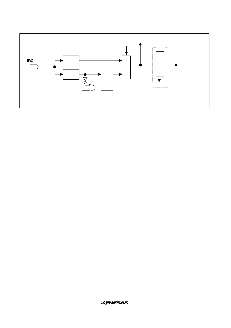
Rev. 2.0, 09/02, page 78 of 732
IRQnS
IRQnES
ISR.IRQnF
pins
RESIRQn
Level
detection
Edge
detection
S
Q
R
Selection
determination
CPU interrupt
request
DTC
DTC starting request
(Acceptance of IRQn interrupt/DTC transfer end/
writing 0 after reading IRQnF = 1)
Figure 6.2 Block Diagram of IRQ7 to IRQ0 Interrupts Control
6.4.2
On-Chip Peripheral Module Interrupts
On-chip peripheral module interrupts are interrupts generated by the following on-chip peripheral
modules.
As a different interrupt vector is assigned to each interrupt source, the exception service routine
does not have to decide which interrupt has occurred. Priority levels between 0 and 15 can be
assigned to individual on-chip peripheral modules in interrupt priority registers A to J (IPRA to
IPRJ). On-chip peripheral module interrupt exception processing sets the interrupt mask level bits
(I3 to I0) in the status register (SR) to the priority level value of the on-chip peripheral module
interrupt that was accepted.
6.4.3
User Break Interrupt
A user break interrupt has a priority of level 15, and occurs when the break condition set in the
user break controller (UBC) is satisfied. User break interrupt requests are detected by edge and are
held until accepted. User break interrupt exception processing sets the interrupt mask level bits (I3
to I0) in the status register (SR) to level 15. For more details about the user break interrupt, see
section 7, User Break Controller.
6.4.4
H-UDI Interrupt
Hitachi user debug interface (H-UDI) interrupt has a priority level of 15, and occurs when an H-
UDI interrupt instruction is serially input. H-UDI interrupt requests are detected by edge and are
held until accepted. H-UDI exception processing sets the interrupt mask level bits (I3-I0) in the
status register (SR) to level 15. For more details about the H-UDI interrupt, see section 22, Hitachi
User Debug Interface.

Rev. 2.0, 09/02, page 79 of 732
6.5
Interrupt Exception Processing Vectors Table
Table 6.2 lists interrupt sources and their vector numbers, vector table address offsets and interrupt
priorities.
Each interrupt source is allocated a different vector number and vector table address offset. Vector
table addresses are calculated from the vector numbers and address offsets. In interrupt exception
processing, the exception service routine start address is fetched from the vector table indicated by
the vector table address. For the details of calculation of vector table address, see table 5.4,
Calculating Exception Processing Vector Table Addresses in the section 5, Exception Processing.
IRQ interrupts and on-chip peripheral module interrupt priorities can be set freely between 0 and
15 for each pin or module by setting interrupt priority registers A to J (IPRA to IPRJ). However,
the smaller vector number has interrupt source, the higher priority ranking is assigned among two
or more interrupt sources specified by the same IPR, and the priority ranking cannot be changed.
A power-on reset assigns priority level 0 to IRQ interrupts and on-chip peripheral module
interrupts. If the same priority level is assigned to two or more interrupt sources and interrupts
from those sources occur simultaneously, they are processed by the default priority order indicated
in table 6.2.
Table 6.2 Interrupt Exception Processing Vectors and Priorities
Interrupt
Source
Name
Vector
No.
Vector Table
Starting Address IPR
Default
Priority
External pin
NMI
11
H'0000002C
--
High
User break
12
H'00000030
--
H-UDI
14
H'00000038
--
--
Reserved by system 15
H'0000003C
--
IRQ0
64
H'00000100
IPRA15 to IPRA12
IRQ1
65
H'00000104
IPRA11 to IPRA8
IRQ2
66
H'00000108
IPRA7 to IPRA4
IRQ3
67
H'0000010C
IPRA3 to IPRA0
IRQ4
68
H'00000110
IPRB15 to IPRB12
IRQ5
69
H'00000114
IPRB11 to IPRB8
IRQ6
70
H'00000118
IPRB7 to IPRB4
Interrupts
IRQ7
71
H'0000011C
IPRB3 to IPRB0
DEI0
72
H'00000120
IPRC15 to IPRC12
DEI1
76
H'00000130
IPRC11 to IPRC8
DEI2
80
H'00000140
IPRC7 to IPRC4
DMAC
DEI3
84
H'00000150
IPRC3 to IPRC0
Low

Rev. 2.0, 09/02, page 80 of 732
Interrupt
Source
Name
Vector
No.
Vector Table
Starting Address IPR
Default
Priority
TGIA_0
88
H'00000160
IPRD15 to IPRD12
High
TGIB_0
89
H'00000164
TGIC_0
90
H'00000168
TGID_0
91
H'0000016C
MTU channel 0
TCIV_0
92
H'00000170
IPRD11 to IPRD8
TGIA_1
96
H'00000180
IPRD7 to IPRD4
TGIB_1
97
H'00000184
TCIV_1
100
H'00000190
IPRD3 to IPRD0
MTU channel 1
TCIU_1
101
H'00000194
MTU channel 2 TGIA_2
104
H'000001A0
IPRE15 to IPRE12
TGIB_2
105
H'000001A4
TCIV_2
108
H'000001B0
IPRE11 to IPRE8
TCIU_2
109
H'000001B4
MTU channel 3 TGIA_3
112
H'000001C0
IPRE7 to IPRE4
TGIB_3
113
H'000001C4
TGIC_3
114
H'000001C8
TGID_3
115
H'000001CC
TCIV_3
116
H'000001D0
IPRE3 to IPRE0
MTU channel 4 TGIA_4
120
H'000001E0
IPRF15 to IPRF12
TGIB_4
121
H'000001E4
TGIC_4
122
H'000001E8
TGID_4
123
H'000001EC
TCIV_4
124
H'000001F0
IPRF11 to IPRF8
SCI channel 0
ERI_0
128
H'00000200
IPRF7 to IPRF4
RXI_0
129
H'00000204
TXI_0
130
H'00000208
TEI_0
131
H'0000020C
SCI channel 1
ERI_1
132
H'00000210
IPRF3 to IPRF0
RXI_1
133
H'00000214
TXI_1
134
H'00000218
TEI_1
135
H'0000021C
A/D
ADI0
136
H'00000220
IPRG15 to IPRG12
ADI1
137
H'00000224
Low

Rev. 2.0, 09/02, page 81 of 732
Interrupt
Source
Name
Vector
No.
Vector Table
Starting Address IPR
Default
Priority
DTC
SWDTEND
140
H'00000230
IPRG11 to IPRG8
High
CMT
CMI0
144
H'00000240
IPRG7 to IPRG4
CMI1
148
H'00000250
IPRG3 to IPRG0
Watchdog
timer
ITI
152
H'00000260
IPRH15 to IPRH12
Reserved by system 153
H'00000264
I/O (MTU)
MTUOEI
156
H'00000270
IPRH11 to IPRH8
Reserved by system 160 to
167
H'00000290 to
H'0000029C
SCI channel 2
ERI_2
168
H'000002A0
IPRI15 to IPRI12
RXI_2
169
H'000002A4
TXI_2
170
H'000002A8
TEI_2
171
H'000002AC
SCI channel 3
ERI_3
172
H'000002B0
IPRI11 to IPRI8
RXI_3
173
H'000002B4
TXI_3
174
H'000002B8
TEI_3
175
H'000002BC
Reserved by system 176 to
188
H'000002C0 to
H'000002FC
IIC
ICI
192
H'00000300
IPRJ7 to IPRJ4
Reserved by system 196 to
247
H'00000304 to
H'000003DC
Low

Rev. 2.0, 09/02, page 82 of 732
6.6
Interrupt Operation
6.6.1
Interrupt Sequence
The sequence of interrupt operations is explained below. Figure 6.3 is a flowchart of the
operations.
1. The interrupt request sources send interrupt request signals to the interrupt controller.
2. The interrupt controller selects the highest priority interrupt in the interrupt requests sent,
according to the priority levels set in interrupt priority level setting registers A to J (IPRA to
IPRJ). Interrupts that have lower-priority than that of the selected interrupt are ignored.* If
interrupts that have the same priority level or interrupts within a same module occur
simultaneously, the interrupt with the highest priority is selected according to the default
priority order indicated in table 6.2.
3. The interrupt controller compares the priority level of the selected interrupt request with the
interrupt mask bits (I3 to I0) in the CPU's status register (SR). If the request priority level is
equal to or less than the level set in I3 to I0, the request is ignored. If the request priority level
is higher than the level in bits I3 to I0, the interrupt controller accepts the interrupt and sends
an interrupt request signal to the CPU.
4. When the interrupt controller accepts an interrupt, a low level is output from the
IRQOUT pin.
5. The CPU detects the interrupt request sent from the interrupt controller when CPU decodes the
instruction to be executed. Instead of executing the decoded instruction, the CPU starts
interrupt exception processing (figure 6.5).
6. SR and PC are saved onto the stack.
7. The priority level of the accepted interrupt is copied to the interrupt mask level bits (I3 to I0) in
the status register (SR).
8. When the accepted interrupt is sensed by level or is from an on-chip peripheral module, a high
level is output from the
IRQOUT pin. When the accepted interrupt is sensed by edge, a high
level is output from the
IRQOUT pin at the moment when the CPU starts interrupt exception
processing instead of instruction execution as noted in (5) above. However, if the interrupt
controller accepts an interrupt with a higher priority than the interrupt just to be accepting, the
IRQOUT pin holds low level.
9. The CPU reads the start address of the exception service routine from the exception vector
table for the accepted interrupt, jumps to that address, and starts executing the program. This
jump is not a delay branch.
Note: * Interrupt requests that are designated as edge-detect type are held pending until the
interrupt requests are accepted. IRQ interrupts, however, can be cancelled by accessing the
IRQ status register (ISR). Interrupts held pending due to edge detection are cleared by a
power-on reset or a manual reset.
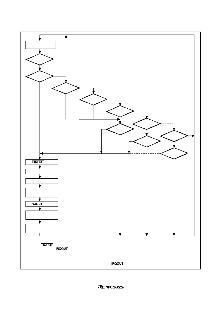
Rev. 2.0, 09/02, page 83 of 732
Program
execution state
Interrupt?
NMI?
User break?
I3 to I0
level 14?
Level 14
interrupt?
Level 1
interrupt?
I3 to I0
level 13?
I3 to I0
=
level 0?
No
Yes
No
No
No
No
No
No
No
No
Yes
Yes
Yes
Yes
Yes
Yes
Yes
Yes
= low
*
1
Save SR to stack
Save PC to stack
Copy accept-interrupt
level to I3 to I0
= high
Read exception
vector table
Branch to exception
service routine
*
2
H-UDI
interrupt?
No
Yes
Level 15
interrupt?
Notes: I3 to I0 are Interrupt mask bits of status register (SR) in the CPU
1.
is the same signal as interrupt request signal to the CPU (see figure 6.1).
Therefore,
is output when the request priority level is higher than the level in bits I3≠I0 of SR.
2.
When the accepted interrupt is sensed by edge, a high level is output from the IRQOUT pin at the moment when
the CPU starts interrupt exception processing instead of instruction execution (namely, before saving SR to stack).
However, if the interrupt controller accepts an interrupt with a higher priority than the interrupt just to be accepted
and has output an interrupt request to the CPU, the
pin holds low level.
Figure 6.3 Interrupt Sequence Flowchart

Rev. 2.0, 09/02, page 84 of 732
6.6.2
Stack after Interrupt Exception Processing
Figure 6.4 shows the stack after interrupt exception processing.
32 bits
32 bits
PC
*
1
SR
Address
4n≠8
4n≠4
4n
SP
*
2
Notes: 1. PC: Start address of the next instruction (return destination instruction) after the executing
instruction
2. Always make sure that SP is a multiple of 4
Figure 6.4 Stack after Interrupt Exception Processing

Rev. 2.0, 09/02, page 85 of 732
6.7
Interrupt Response Time
Table 6.3 lists the interrupt response time, which is the time from the occurrence of an interrupt
request until the interrupt exception processing starts and fetching of the first instruction of the
interrupt service routine begins. Figure 6.5 shows an example of the pipeline operation when an
IRQ interrupt is accepted.
Table 6.3 Interrupt Response Time
Number of States
Item
NMI, Peripheral
Module
IRQ
Remarks
DMAC/DTC active
judgment
0 or 1
1
1 state required for interrupt
signals for which
DMAC/DTC activation is
possible
Interrupt priority judgment
and comparison with SR
mask bits
2
3
Wait for completion of
sequence currently being
executed by CPU
X (
0)
X (
0)
The longest sequence is for
interrupt or address-error
exception processing (X = 4
+ m1 + m2 + m3 + m4). If an
interrupt-masking instruction
follows, however, the time
may be even longer.
Time from start of interrupt
exception processing until
fetch of first instruction of
exception service routine
starts
5 + m1 + m2 + m3
5 + m1 + m2 + m3
Performs the saving PC and
SR, and vector address
fetch.
Total: (7 or 8) + m1 +
m2 + m3+X
9 + m1 + m2 +
m3 + X
Minimum:
10
12
0.20 to 0.24 µs at 50 MHz
Interrupt
response
time
Maximum:
12 + 2 (m1 + m2
+ m3) + m4
13 + 2 (m1 + m2
+ m3) + m4
0.38 to 0.40 µs at 50 MHz
*
Note:
m1 to m4 are the number of states needed for the following memory accesses.
m1: SR save (longword write)
m2: PC save (longword write)
m3: Vector address read (longword read)
m4: Fetch first instruction of interrupt service routine
*
0.38 to 0.40 µs at 50 MHz is the value in the case that m1 = m2 = m3 = m4 = 1.
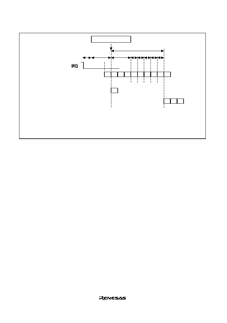
Rev. 2.0, 09/02, page 86 of 732
F
D
E
M
E
E
M
M
E
E
E
F
D
F
3
1
3
Interrupt acceptance
m1 m2 1 m3 1
5 + m1 + m2 + m3
Instruction (instruction
replaced by interrupt
exception processing)
Overrun fetch
Interrupt service routine
start instruction
F: Instruction fetch (instruction fetched from memory where program is stored).
D: Instruction decoding (fetched instruction is decoded).
E: Instruction execution (data operation and address calculation is performed according to the results
of decoding).
M: Memory access (data in memory is accessed).
Figure 6.5 Example of the Pipeline Operation when an IRQ Interrupt is Accepted
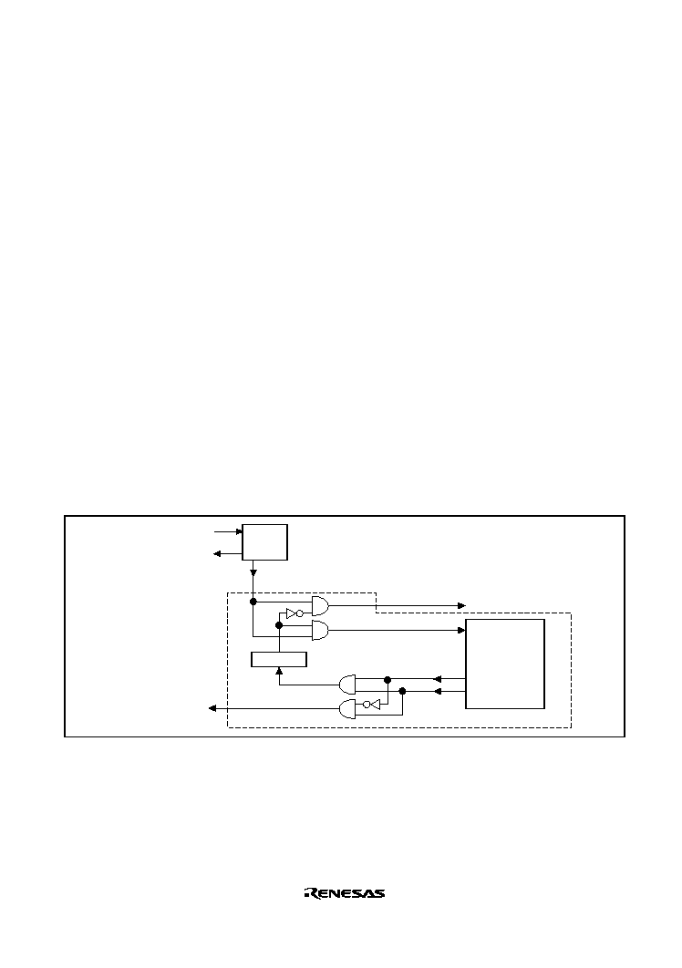
Rev. 2.0, 09/02, page 87 of 732
6.8
Data Transfer with Interrupt Request Signals
The following data transfers can be done using interrupt request signals:
∑
Activate DMAC only, CPU interrupts do not occur
∑
Activate DTC only, CPU interrupts according to DTC settings
Interrupt sources that are activated by DMAC are masked without being input to INTC. Mask
condition is as follows:
Mask condition = DME
∑
(DE0
∑
interrupt source select0 + DE1
∑
interrupt source select1 + DE2
∑
interrupt source select2 + DE3
∑
interrupt source select3)
The INTC masks CPU interrupts when the corresponding DTE bit is 1. The conditions for clearing
DTE and interrupt source flag are listed below.
DTE clear condition = DTC transfer end
∑
DTECLR
Interrupt source flag clear condition = DTC transfer end
∑
DTECLR+DMAC transfer end
Where: DTECLR = DISEL + counter 0.
Figure 6.6 shows a control block diagram.
Interrupt source
flag clear (by DTC)
CPU interrupt request
DTC activation
request
DTECLR
Transfer end
DTER
DMAC
DTE clear
Interrupt source
Interrupt source
(not designated as DMAC activation source)
Interrupt source
Flag clear (by DMAC)
Figure 6.6 Interrupt Control Block Diagram

Rev. 2.0, 09/02, page 88 of 732
6.8.1
Handling Interrupt Request Signals as Sources for DTC Activating and CPU
Interrupt, but Not DMAC Activating
1. Do not select DMAC activating sources or clear the DTE bit to 0.
2. For DTC, set the corresponding DTE bits and DISEL bits to 1.
3. Activating sources are applied to the DTC when interrupts occur.
4. When the DTC performs a data transfer, it clears the DTE bit to 0 and sends an interrupt
request to the CPU. The activating source is not cleared.
5.
The CPU clears interrupt sources in the interrupt processing routine then confirms the transfer
counter value. When the transfer counter value is not 0, the CPU sets the DTE bit to 1 and
allows the next data transfer. If the transfer counter value = 0, the CPU performs the
necessary end processing in the interrupt processing routine.
6.8.2
Handling Interrupt Request Signals as Sources for Activating DMAC, but Not
CPU Interrupt and DTC Activating
1. Select DMAC activating sources and set the DME bit to 1. Then, CPU interrupt and DTC
activating sources are masked regardless of the settings of the interrupt priority register and the
DTC register.
2. Activating sources are applied to the DMAC when interrupts occur.
3. The DMAC clears the interrupt sources when starting transfer.
6.8.3
Handling Interrupt Request Signals as Source for DTC Activating, but Not CPU
Interrupt and DMAC Activating
1. Do not select DMAC activating sources or clear the DME bit to 0.
2. For DTC, set the corresponding DTE bits to 1 and clear the DISEL bits to 0.
3. Activating sources are applied to the DTC when interrupts occur.
4. When the DTC performs a data transfer, it clears the activating source. An interrupt request is
not sent to the CPU, because the DTE bit is hold to 1.
5. However, when the transfer counter value = 0 the DTE bit is cleared to 0 and an interrupt
request is sent to the CPU.
6. The CPU performs the necessary end processing in the interrupt processing routine.

Rev. 2.0, 09/02, page 89 of 732
6.8.4
Handling Interrupt Request Signals as Source for CPU Interrupt but Not DMAC
and DTC Activating
1
Do not select DMAC activating sources or clear the DME bit to 0.
2. For DTC, clear the corresponding DTE bits to 0.
3. When interrupts occur, interrupt requests are sent to the CPU.
4. The CPU clears the interrupt source and performs the necessary processing in the interrupt
processing routine.

Rev. 2.0, 09/02, page 90 of 732

UBC0001A_000020010800
Rev. 2.0, 09/02, page 91 of 732
Section 7 User Break Controller (UBC)
The user break controller (UBC) provides functions that make program debugging easier. By
setting break conditions in the UBC, a user break interrupt is generated according to the contents
of the bus cycle generated by the CPU or DMAC/DTC. This function makes it easy to design an
effective self-monitoring debugger, and customers of the chip can easily debug their programs
without using a large in-circuit emulator.
7.1
Overview
∑
There are 5 types of break compare conditions as follows:
Address
CPU cycle or DMAC/DTC cycle
Instruction fetch or data access
Read or write
Operand size: longword/word/byte
∑
User break interrupt generated upon satisfying break conditions
∑
User break interrupt generated before an instruction is executed by selecting break in the CPU
instruction fetch.
∑
Module standby mode can be set
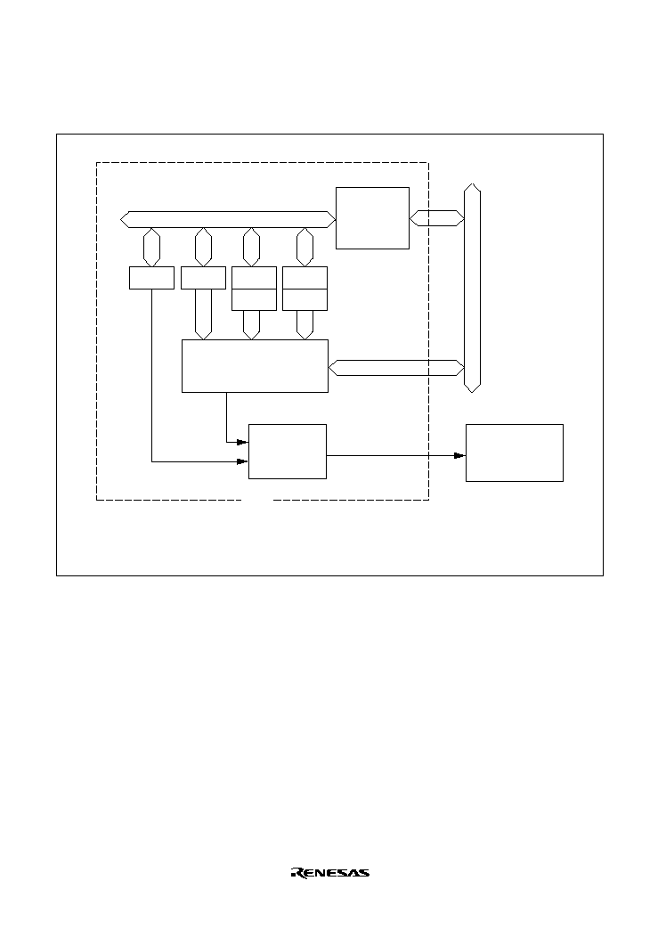
Rev. 2.0, 09/02, page 92 of 732
Figure 7.1 shows a block diagram of the UBC.
Module bus
UBBR
UBAMRH
UBAMRL
UBARH
UBARL
Break condition
comparator
User break
interrupt
generating
circuit
Bus
interface
Internal bus
Interrupt request
Interrupt controller
UBARH, UBARL:
User break address registers H, L
UBAMRH, UBAMRL: User break address mask registers H, L
UBBR:
User break bus cycle register
UBCR:
User break control register
UBCR
UBC
Figure 7.1 User Break Controller Block Diagram

Rev. 2.0, 09/02, page 93 of 732
7.2
Register Descriptions
The UBC has the following registers. For details on register addresses and register states during
each processing, refer to section 25, List of Registers.
∑
User break address register H (UBARH)
∑
User break address register L (UBARL)
∑
User break address mask register H (UBAMRH)
∑
User break address mask register L (UBAMRL)
∑
User break bus cycle register (UBBR)
∑
User break control register (UBCR)
7.2.1
User Break Address Register (UBAR)
The user break address register (UBAR) consists of two registers: user break address register H
(UBARH) and user break address register L (UBARL). Both are 16-bit readable/writable registers.
UBARH specifies the upper bits (bits 31 to 16) of the address for the break condition, while
UBARL specifies the lower bits (bits 15 to 0).
The initial value of UBAR is H
00000000.
∑
UBARH Bits 15 to 0: specifies user break address 31 to 16 (UBA31 to UBA16)
∑
UBARL Bits 15 to 0: specifies user break address 15 to 0 (UBA15 to UBA0)
7.2.2
User Break Address Mask Register (UBAMR)
The user break address mask register (UBAMR) consists of two registers: user break address mask
register H (UBAMRH) and user break address mask register L (UBAMRL). Both are 16-bit
readable/writable registers. UBAMRH specifies whether to mask any of the break address bits set
in UBARH, and UBAMRL specifies whether to mask any of the break address bits set in UBARL.
∑
UBAMRH Bits 15 to 0: specifies user break address mask 31 to 16 (UBM31 to UBM16)
∑
UBAMRL Bits 15 to 0: specifies user break address mask 15 to 0 (UBM15 to UBM0)

Rev. 2.0, 09/02, page 94 of 732
Bit
Bit Name
Initial Value
R/W
Description
UBAMRH
Bit 15 to 0
UBM31 to
UBM16
All 0
R/W
User Break Address Mask 31 to 16
0: Corresponding UBA bit is included in the
break conditions
1: Corresponding UBA bit is not included in
the break conditions
UBAMRL
Bit 15 to 0
UBM15 to
UBM0
All 0
R/W
User Break Address Mask 15 to 0
0: Corresponding UBA bit is included in the
break conditions
1: Corresponding UBA bit is not included in
the break conditions
7.2.3
User Break Bus Cycle Register (UBBR)
The user break bus cycle register (UBBR) is a 16-bit readable/writable register that sets the four
break conditions.
Bit
Bit Name Initial Value
R/W
Description
15 to 8
--
All 0
R
Reserved bits
These bits are always read as 0. The write value
should always be 0.
7
6
CP1
CP0
0
0
R/W
R/W
CPU Cycle/DMAC, DTC Cycle Select 1 and 0
These bits specify break conditions for CPU cycles or
DMAC/DTC cycles.
00: No user break interrupt occurs
01: Break on CPU cycles
10: Break on DTC or DMAC cycles
11: Break on both CPU and DMAC or DTC cycles
5
4
ID1
ID0
0
0
R/W
R/W
Instruction Fetch/Data Access Select1 and 0
These bits select whether to break on instruction fetch
and/or data access cycles.
00: No user break interrupt occurs
01: Break on instruction fetch cycles
10: Break on data access cycles
11: Break on both instruction fetch and data access
cycles

Rev. 2.0, 09/02, page 95 of 732
Bit
Bit Name Initial Value
R/W
Description
3
2
RW1
RW0
0
0
R/W
R/W
Read/Write Select 1 and 0
These bits select whether to break on read and/or
write cycles
00: No user break interrupt occurs
01: Break on read cycles
10: Break on write cycles
11: Break on both read and write cycles
1
0
SZ1
SZ0
0
0
R/W
R/W
Operand Size Select 1 and 0
*
These bits select operand size as a break condition.
00: Operand size is not a break condition
01: Break on byte access
10: Break on word access
11: Break on longword access
Note:
*
When breaking on an instruction fetch, clear the SZ0 bit to 0. All instructions are considered
to be accessed in word-size (even when there are instructions in on-chip memory and two
instruction fetches are performed simultaneously in one bus cycle).
Operand size is word for instructions or determined by the operand size specified for the
CPU/DTC, DMAC data access. It is not determined by the bus width of the space being
accessed.
7.2.4
User Break Control Register (UBCR)
The user break control register (UBCR) is a 16-bit readable/writable register that enables or
disables user break interrupts.
Bit
Bit Name
Initial Value
R/W
Description
15 to
1
--
All 0
R
Reserved bits
These bits are always read as 0. The write value
should always be 0.
0
UBID
0
R/W
User Break Disable
Enables or disables user break interrupt request
generation in the event of a user break condition
match.
0: User break interrupt request is enabled
1: User break interrupt request is disabled

Rev. 2.0, 09/02, page 96 of 732
7.3
Operation
7.3.1
Flow of the User Break Operation
The flow from setting of break conditions to user break interrupt exception processing is described
below:
1. The user break addresses are set in the user break address register (UBAR), the desired masked
bits in the addresses are set in the user break address mask register (UBAMR) and the breaking
bus cycle type is set in the user break bus cycle register (UBBR). If even one of the three
groups of the UBBR's CPU cycle/DMAC, DTC cycle select bits (CP1, CP0), instruction
fetch/data access select bits (ID1, ID0), and read/write select bits (RW1, RW0) is set to 00 (no
user break generated), no user break interrupt will be generated even if all other conditions are
satisfied. When using user break interrupts, always be certain to establish bit conditions for all
of these three groups.
2. The UBC uses the method shown in figure 7.2 to determine whether set conditions have been
satisfied or not. When the set conditions are satisfied, the UBC sends a user break interrupt
request signal to the interrupt controller (INTC).
3. The interrupt controller checks the accepted user break interrupt request signal's priority level.
The user break interrupt has priority level 15, so it is accepted only if the interrupt mask level
in bits I3 to I0 in the status register (SR) is 14 or lower. When the I3 to I0 bit level is 15, the
user break interrupt cannot be accepted but it is held pending until user break interrupt
exception processing can be carried out. Consequently, user break interrupts within NMI
exception service routines cannot be accepted, since the I3 to I0 bit level is 15. However, if the
I3 to I0 bit level is changed to 14 or lower at the start of the NMI exception service routine,
user break interrupts become acceptable thereafter. See section 6, Interrupt Controller, for the
details on the handling of priority levels.
4. The INTC sends the user break interrupt request signal to the CPU, which begins user break
interrupt exception processing upon receipt. See section 6.6, Interrupt Operation, for the details
on interrupt exception processing.
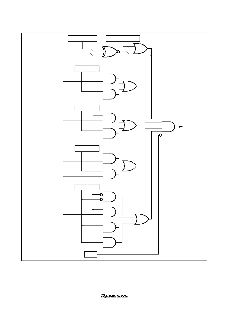
Rev. 2.0, 09/02, page 97 of 732
UBARH/UBARL
UBAMRH/UBAMRL
Internal address
bits 31≠0
CPU cycle
DMAC/DTC cycle
Instruction fetch
Data access
Read cycle
Write cycle
Byte size
Word size
Longword size
32
32
32
32
32
CP1
CP0
ID1
ID0
RW1
RW0
SZ1
SZ0
User
break
interrupt
UBID
Figure 7.2 Break Condition Determination Method

Rev. 2.0, 09/02, page 98 of 732
7.3.2
Break on On-Chip Memory Instruction Fetch Cycle
Data in on-chip memory (on-chip ROM and/or RAM) is always accessed as 32-bits data in one
bus cycle. Therefore, two instructions can be retrieved in one bus cycle when fetching instructions
from on-chip memory. At such times, only one bus cycle is generated, but it is possible to cause
independent breaks by setting the start addresses of both instructions in the user break address
register (UBAR). In other words, when wanting to effect a break using the latter of two addresses
retrieved in one bus cycle, set the start address of that instruction in UBAR. The break will occur
after execution of the former instruction.
7.3.3
Program Counter (PC) Values Saved
Break on Instruction Fetch: The program counter (PC) value saved to the stack in user break
interrupt exception processing is the address that matches the break condition. The user break
interrupt is generated before the fetched instruction is executed. If a break condition is set in an
instruction fetch cycle placed immediately after a delayed branch instruction (delay slot), or on an
instruction that follows an interrupt-disabled instruction, however, the user break interrupt is not
accepted immediately, but the break condition establishing instruction is executed. The user break
interrupt is accepted after execution of the instruction that has accepted the interrupt. In this case,
the PC value saved is the start address of the instruction that will be executed after the instruction
that has accepted the interrupt.
Break on Data Access (CPU/DTC, DMAC): The program counter (PC) value is the top address
of the next instruction after the last instruction executed before the user break exception
processing started. When data access (CPU/DTC, DMAC) is set as a break condition, the place
where the break will occur cannot be specified exactly. The break will occur at the instruction
fetched close to where the data access that is to receive the break occurs.

Rev. 2.0, 09/02, page 99 of 732
7.4
Examples of Use
Break on CPU Instruction Fetch Cycle
1. Register settings: UBARH = H'0000
UBARL = H'0404
UBBR = H'0054
UBCR = H'0000
Conditions set:
Address: H'00000404
Bus cycle: CPU, instruction fetch, read
(operand size is not included in conditions)
Interrupt requests enabled
A user break interrupt will occur before the instruction at address H'00000404. If it is possible
for the instruction at H'00000402 to accept an interrupt, the user break exception processing
will be executed after execution of that instruction. The instruction at H'00000404 is not
executed. The PC value saved is H'00000404.
2. Register settings: UBARH = H'0015
UBARL = H'389C
UBBR = H'0058
UBCR = H'0000
Conditions set:
Address: H'0015389C
Bus cycle: CPU, instruction fetch, write
(operand size is not included in conditions)
Interrupt requests enabled
A user break interrupt does not occur because the instruction fetch cycle is not a write cycle.
3. Register settings: UBARH = H'0003
UBARL = H'0147
UBBR = H'0054
UBCR = H'0000
Conditions set:
Address: H'00030147
Bus cycle: CPU, instruction fetch, read
(operand size is not included in conditions)
Interrupt requests enabled
A user break interrupt does not occur because the instruction fetch was performed for an even
address. However, if the first instruction fetch address after the branch is an odd address set by
these conditions, user break interrupt exception processing will be carried out after address
error exception processing.

Rev. 2.0, 09/02, page 100 of 732
Break on CPU Data Access Cycle
1. Register settings: UBARH = H'0012
UBARL = H'3456
UBBR = H'006A
UBCR = H'0000
Conditions set:
Address: H'00123456
Bus cycle: CPU, data access, write, word
Interrupt requests enabled
A user break interrupt occurs when word data is written into address H'00123456.
2. Register settings: UBARH = H'00A8
UBARL = H'0391
UBBR = H'0066
UBCR = H'0000
Conditions set:
Address: H'00A80391
Bus cycle: CPU, data access, read, word
Interrupt requests enabled
A user break interrupt does not occur because the word access was performed on an even
address.
Break on DMAC/DTC Cycle
1. Register settings: UBARH = H'0076
UBARL = H'BCDC
UBBR = H'00A7
UBCR = H'0000
Conditions set:
Address: H'0076BCDC
Bus cycle: DMAC/DTC, data access, read, longword
Interrupt requests enabled
A user break interrupt occurs when longword data is read from address H'0076BCDC.
2. Register settings: UBARH = H'0023
UBARL = H'45C8
UBBR = H'0094
UBCR = H'0000
Conditions set:
Address: H'002345C8
Bus cycle: DMAC/DTC, instruction fetch, read
(operand size is not included in conditions)
Interrupt requests enabled
A user break interrupt does not occur because no instruction fetch is performed in the
DMAC/DTC cycle.

Rev. 2.0, 09/02, page 101 of 732
7.5
Usage Notes
7.5.1
Simultaneous Fetching of Two Instructions
Two instructions may be simultaneously fetched in instruction fetch operation. Once a break
condition is set on the latter of these two instructions, a user break interrupt will occur before the
latter instruction, even though the contents of the UBC registers are modified to change the break
conditions immediately after the fetching of the former instruction.
7.5.2
Instruction Fetches at Branches
When a conditional branch instruction or TRAPA instruction causes a branch, the order of
instruction fetching and execution is as follows:
1. When branching with a conditional branch instruction: BT and BF instructions
When branching with a TRAPA instruction:
TRAPA instruction
a. Instruction fetch order
Branch instruction fetch
next instruction overrun fetch
overrun fetch of instruction
after the next
branch destination instruction fetch
b. Instruction execution order
Branch instruction execution
branch destination instruction execution
2. When branching with a delayed conditional branch instruction: BT/S and BF/S instructions
a. Instruction fetch order
Branch instruction fetch
next instruction fetch (delay slot)
overrun fetch of
instruction after the next
branch destination instruction fetch
b. Instruction execution order
Branch instruction execution
delay slot instruction execution
branch destination
instruction execution
Thus, when a conditional branch instruction or TRAPA instruction causes a branch, the branch
destination instruction will be fetched after an overrun fetch of the next instruction or the
instruction after the next. However, as the instruction that is the object of the break does not break
until fetching and execution of the instruction have been confirmed, the overrun fetches described
above do not become objects of a break.
If data accesses are also included in break conditions besides instruction fetch, a break will occur
because the instruction overrun fetch is also regarded as satisfying the data break condition.

Rev. 2.0, 09/02, page 102 of 732
7.5.3
Contention between User Break and Exception Processing
If a user break is set for the fetch of a particular instruction, and exception processing with higher
priority than a user break is in contention and is accepted in the decode stage for that instruction
(or the next instruction), user break exception processing may not be performed after completion
of the higher-priority exception service routine (on return by RTE).
Thus, if a user break condition is specified to the branch destination instruction fetch after a
branch (BRA, BRAF, BT, BF, BT/S, BF/S, BSR, BSRF, JMP, JSR, RTS, RTE, exception
processing), and that branch instruction accepts an exception processing with higher priority than
a user break interrupt, user break exception processing is not performed after completion of the
exception service routine.
Therefore, a user break condition should not be set for the fetch of the branch destination
instruction after a branch.
7.5.4
Break at Non-Delay Branch Instruction Jump Destination
When a branch instruction without delay slot (including exception processing) jumps to the
destination instruction by executing the branch, a user break will not be generated even if a user
break condition has been set for the first jump destination instruction fetch.
7.5.5
Module Standby Mode Setting
The UBC can set the module disable/enable by using the module standby control register 2
(MSTCR2). By releasing the module standby mode, register access becomes to be enabled.
By setting the MSTP0 bit of MSTCR2 to 1, the UBC is in the module standby mode in which the
clock supply is halted. See section 24, Power-Down State, for further details.

DTCSH21A_010020020700
Rev. 2.0, 09/02, page 103 of 732
Section 8 Data Transfer Controller (DTC)
This LSI includes a data transfer controller (DTC). The DTC can be activated by an interrupt or
software, to transfer data.
Figure 8.1 shows a block diagram of the DTC.
The DTC's register information is stored in the on-chip RAM. When the DTC is used, the RAME
bit in SYSCR must be set to 1.
8.1
Features
∑
Transfer possible over any number of channels
∑
Three transfer modes
Normal, repeat, and block transfer modes available
∑
One activation source can trigger a number of data transfers (chain transfer)
∑
Direct specification of 32-bit address space possible
∑
Activation by software is possible
∑
Transfer can be set in byte, word, or longword units
∑
The interrupt that activated the DTC can be requested to the CPU
∑
Module standby mode can be set
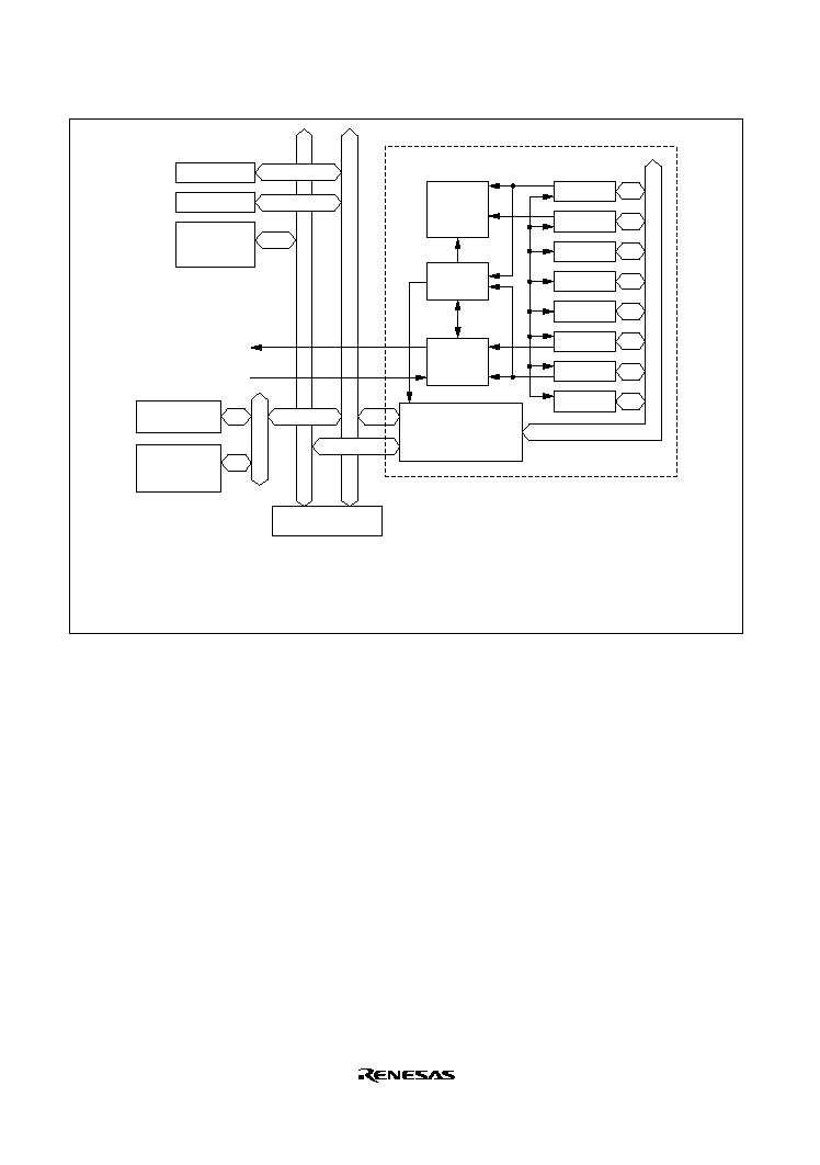
Rev. 2.0, 09/02, page 104 of 732
On-chip ROM
On-chip RAM
External
memory
External device
(memory-
mapped)
On-chip
peripheral
module
CPU interrupt request
source clear control
Register
control
DTMR
DTCR
DTSAR
DTDAR
DTIAR
DTER
DTCSR
DTBR
DTC
DTC module bus
Activation
control
Internal bus
Peripheral bus
External bus
Request
priority
control
Interrupt request
Bus interface
Bus controller
Legend:
DTMR: DTC mode register
DTCR: DTC transfer count register
DTSAR: DTC source address register
DTDAR: DTC destination address register
DTIAR: DTC initial address register
DTER:
DTC enable register
DTCSR: DTC control/status register
DTBR:
DTC information base register
Figure 8.1 Block Diagram of DTC

Rev. 2.0, 09/02, page 105 of 732
8.2
Register Descriptions
DTC has the following registers.
∑
DTC mode register (DTMR)
∑
DTC source address register (DTSAR)
∑
DTC destination address register (DTDAR)
∑
DTC initial address register (DTIAR)
∑
DTC transfer count register A (DTCRA)
∑
DTC transfer count register B (DTCRB)
These six registers cannot be directly accessed from the CPU.
When activated, the DTC transfer desired set of register information that is stored in an on-chip
RAM to the corresponding DTC registers. After the data transfer, it writes a set of updated register
information back to the RAM.
∑
DTC enable register A (DTEA)
∑
DTC enable register B (DTEB)
∑
DTC enable register C (DTEC)
∑
DTC enable register D (DTED)
∑
DTC enable register E (DTEE)
∑
DTC enable register G (DTEG)
∑
DTC control/status register (DTCSR)
∑
DTC information base register (DTBR)
For details on register addresses and register states during each processing, refer to section 25, List
of Registers.

Rev. 2.0, 09/02, page 106 of 732
8.2.1
DTC Mode Register (DTMR)
DTMR is a 16-bit register that selects the DTC operating mode.
Bit
Bit Name
Initial Value
R/W
Description
15
14
SM1
SM0
Undefined
Undefined
--
--
Source Address Mode 1 and 0
These bits specify a DTSAR operation after a data
transfer.
0x: DTSAR is fixed
10: DTSAR is incremented after a transfer
(by +1 when Sz 1 and 0 = 00; by +2 when Sz 1
and 0 = 01; by +4 when Sz 1 and 0 = 10)
11: DTSAR is decremented after a transfer
(by ≠1 when Sz 1 and 0 = 00; by ≠2 when Sz 1
and 0 = 01; by ≠4 when Sz 1 and 0 = 10)
13
12
DM1
DM0
Undefined
Undefined
--
--
Destination Address Mode 1 and 0
These bits specify a DTDAR operation after a data
transfer.
0x: DTDAR is fixed
10: DTDAR is incremented after a transfer
(by +1 when Sz 1 and 0 = 00; by +2 when Sz 1
and 0 = 01; by +4 when Sz 1 and 0 = 10)
11: DTDAR is decremented after a transfer
(by ≠1 when Sz 1 and 0 = 00; by ≠2 when Sz 1
and 0 = 01; by ≠4 when Sz 1 and 0 = 10)
11
10
MD1
MD0
Undefined
Undefined
--
--
DTC Mode 1 and 0
These bits specify the DTC transfer mode.
00: Normal mode
01: Repeat mode
10: Block transfer mode
11: Setting prohibited
9
8
Sz1
Sz0
Undefined
Undefined
--
--
DTC Data Transfer Size 1 and 0
Specify the size of data to be transferred.
00: Byte-size transfer
01: Word-size transfer
10: longword-size transfer
11: Setting prohibited

Rev. 2.0, 09/02, page 107 of 732
Bit
Bit Name
Initial Value
R/W
Description
7
DTS
Undefined
--
DTC Transfer Mode Select
Specifies whether the source or the destination is set
to be a repeat area or block area, in repeat mode or
block transfer mode.
0: Destination is repeat area or block area
1: Source is repeat area or block area
6
CHNE
Undefined
--
DTC Chain Transfer Enable
When this bit is set to 1, a chain transfer will be
performed.
0: Chain transfer is canceled
1: Chain transfer is set
In data transfer with CHNE set to 1, determination of
the end of the specified number of transfers, clearing
of the activation source flag, and clearing of DTER is
not performed.
5
DISEL
Undefined
--
DTC Interrupt Select
When this bit is set to 1, a CPU interrupt request is
generated every time a data transfer ends. When this
bit is set to 0, a CPU interrupt request is generated at
the time when the specified number of data transfer
ends.
4
NMIM
Undefined
--
DTC NMI Mode
This bit designates whether to terminate transfers
when an NMI is input during DTC transfers.
0: Terminate DTC transfer upon an NMI
1: Continue DTC transfer until end of transfer being
executed
3
2
1
0
--
--
--
--
Undefined
Undefined
Undefined
Undefined
--
--
--
--
Reserved
These bits have no effect on DTC operation and
should always be written with 0.
X: Don't care

Rev. 2.0, 09/02, page 108 of 732
8.2.2
DTC Source Address Register (DTSAR)
The DTC source address register (DTSAR) is a 32-bit register that specifies the DTC transfer
source address. For the word size transfer, specify an even source address. For the longword size
transfer, specify a multiple-of-four address.
The initial value of DTSAR is undefined.
8.2.3
DTC Destination Address Register (DTDAR)
The DTC destination address register (DTDAR) is a 32-bit register that specifies the DTC transfer
destination address. For the word size transfer, specify an even source address. For the longword
size transfer, specify a multiple-of-four address.
The initial value of DTDAR is undefined.
8.2.4
DTC Initial Address Register (DTIAR)
The DTC initial address register (DTIAR) is a 32-bit register that specifies the initial transfer
source/transfer destination address in repeat mode. In repeat mode, when the DTS bit is set to 1,
specify the initial transfer source address in the repeat area, and when the DTS bit is cleared to 0,
specify the initial transfer destination address in the repeat area.
The initial value of DTIAR is undefined.
8.2.5
DTC Transfer Count Register A (DTCRA)
DTCRA is a 16-bit register that designates the number of times data is to be transferred by the
DTC.
In normal mode, the DTCRA functions as a 16-bit transfer counter (1 to 65536). It is decremented
by 1 every time data is transferred, and transfer ends when the count reaches H'0000. The number
of transfers is 1 when the set value is H'0001, 65535 when it is H'FFFF, and 65536 when it is
H'0000.
In repeat mode, upper 8-bit DTCRAH maintains the transfer count value and lower 8-bit
DTCRAL functions as an 8-bit transfer counter. The number of transfers is 1 when the set value is
DTCRAH = DTCRAL = H'01, 255 when they are H'FF, and 256 when it is H'00.
In block transfer mode, the DTCRA functions as a 16-bit transfer counter. The number of transfers
is 1 when the set value is H'0001, 65535 when it is H'FFFF, and 65536 when it is H'0000.
The initial value of DTCRA is undefined.

Rev. 2.0, 09/02, page 109 of 732
8.2.6
DTC Transfer Count Register B (DTCRB)
The DTCRB is a 16-bit register that designates the block length in block transfer mode. The block
length is 1 when the set value is H'0001, 65535 when it is H'FFFF, and 65536 when it is H'0000.
The initial value of DTCRB is undefined.
8.2.7
DTC Enable Registers (DTER)
DTER which is comprised of six registers, DTEA to DTEE, DTEG, is a register that specifies
DTC activation interrupt sources. The correspondence between interrupt sources and DTE bits is
shown in table 8.1.
Bit
Bit Name
Initial Value
R/W
Description
7
6
5
4
3
2
1
0
DTE
*
7
DTE
*
6
DTE
*
5
DTE
*
4
DTE
*
3
DTE
*
2
DTE
*
1
DTE
*
0
0
0
0
0
0
0
0
0
R/W
R/W
R/W
R/W
R/W
R/W
R/W
R/W
DTC Activation Enable
Setting this bit to 1 specifies the corresponding
interrupt source to a DTC activation source.
[Clearing conditions]
∑
When the DISEL bit is 1 and the data transfer has
ended
∑
When the specified number of transfers have
ended
∑
0 is written to the bit to be cleared after 1 has been
read from the bit
These bits are not cleared when the DISEL bit is 0 and
the specified number of transfers have not ended.
[Setting condition]
1 is written to the bit to be set after a 0 has been read
from the bit
Note:
*
The last character of the DTC enable register's name comes here.
Example: DTEB3 in DTEB, etc.

Rev. 2.0, 09/02, page 110 of 732
8.2.8
DTC Control/Status Register (DTCSR)
The DTCSR is a 16-bit readable/writable register that is used to disable/enable DTC activation by
software and to set the DTC vector addresses for software activation. It also indicates the DTC
transfer status.
Bit
Bit Name
Initial Value
R/W
Description
15
14
13
12
11
--
--
--
--
--
0
0
0
0
0
R
R
R
R
R
Reserved
These bits have no effect on DTC operation and
should always be written with 0.
10
NMIF
0
R/(W)
*
1
NMI Flag Bit
This bit indicates that an NMI interrupt has occurred.
0: No NMI interrupts
[Clearing condition]
∑
Write 0 after reading the NMIF bit
1: NMI interrupt has been generated
When the NMIF bit is set, DTC transfers are not
allowed even if the DTER bit is set to 1. If, however,
a transfer has already started with the NMIM bit of
the DTMR set to 1, execution will continue until that
transfer ends.
9
AE
0
R/(W)
*
1
Address Error Flag
This bit indicates that an address error by the DTC
has occurred.
0: No address error by the DTC
[Clearing condition]
∑
Write 0 after reading the AE bit
1: An address error by the DTC occurred
When the AE bit is set, DTC transfers are not
allowed even if the DTER bit is set to 1.
8
SWDTE
0
R/W
*
2
DTC Software Activation Enable
Setting this bit to 1 activates DTC.
0: DTC activation by software disabled
1: DTC activation by software enabled

Rev. 2.0, 09/02, page 111 of 732
Bit
Bit Name
Initial Value
R/W
Description
7
6
5
4
3
2
1
0
DTVEC7
DTVEC6
DTVEC5
DTVEC4
DTVEC3
DTVEC2
DTVEC1
DTVEC0
0
0
0
0
0
0
0
0
R/W
R/W
R/W
R/W
R/W
R/W
R/W
R/W
DTC Software Activation Vectors 7 to 0
These bits specify the lower eight bits of the vector
addresses for DTC activation by software.
A vector address is calculated as H'0400 + DTVEC
(7:0). Always specify 0 for DTVEC0. For example,
when DTVEC7 to DTVEC0 = H'10, the vector
address is H'0410. When the bit SWDTE is 0, these
bits can be written to.
Notes: 1. For the NMIF and AE bits, only a 0 write after a 1 read is possible.
2. For the SWDTE bit, a 1 write is always possible, but a 0 write is possible only after a 1
is read.
8.2.9
DTC Information Base Register (DTBR)
The DTBR is a 16-bit readable/writable register that specifies the upper 16 bits of the memory
address containing DTC transfer information. Always access the DTBR in word or longword
units. If it is accessed in byte units the register contents will become undefined at the time of a
write, and undefined values will be read out upon reads.
The initial value of DTBR is undefined.
8.3
Operation
8.3.1
Activation Sources
The DTC operates when activated by an interrupt or by a write to DTCSR by software. An
interrupt request can be directed to the CPU or DTC, as designated by the corresponding DTER
bit. At the end of a data transfer (or the last consecutive transfer in the case of chain transfer), the
activation source interrupt flag or corresponding DTER bit is cleared. The activation source flag,
in the case of RXI_2, for example, is the RDRF flag of SCI2.
When a DTC is activated by an interrupt, existing CPU mask level and interrupt controller
priorities have no effect. If there is more than one activation source at the same time, the DTC
operates in accordance with the default priorities.
Figure 8.2 shows a block diagram of activation source control. For details see section 6, Interrupt
Controller (INTC).
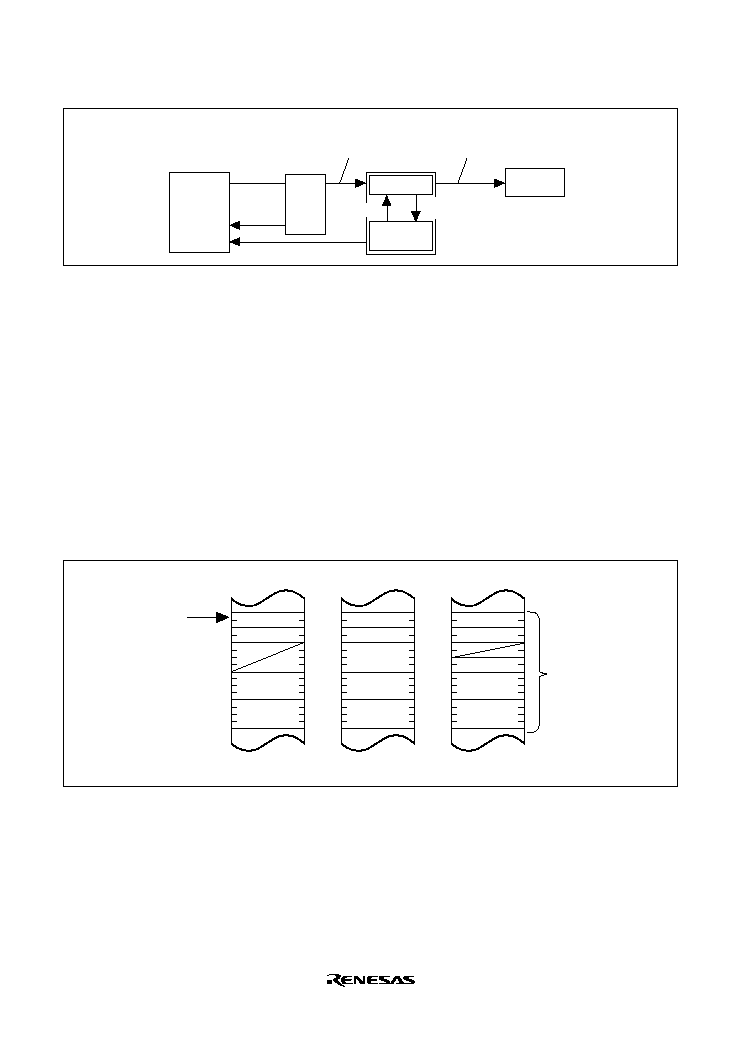
Rev. 2.0, 09/02, page 112 of 732
IRQ
on-chip
peripheral
Interrupt
requests
CPU interrupt requests
(those not designated as
DTC activating sources)
Interrupt requests
(those not designated as
DMAC activating sources)
Source flag clear
Source
flag clear
DTER
INTC
DTC
DTC control
Clear
DTC activation
request
DMAC
Figure 8.2 Activating Source Control Block Diagram
8.3.2
Location of Register Information and DTC Vector Table
Figure 8.3 shows the allocation of register information in memory space. The register information
start addresses are designated by DTBR for the upper 16 bits, and the DTC vector table for the
lower 16 bits.
The allocation in order from the register information start address in normal mode is DTMR,
DTCRA, 4 bytes empty (no effect on DTC operation), DTSAR, then DTDAR. In repeat mode it is
DTMR, DTCRA, DTIAR, DTSAR, and DTDAR. In block transfer mode, it is DTMR, DTCRA, 2
bytes empty (no effect on DTC operation), DTCRB, DTSAR, then DTDAR.
Fundamentally, certain RAM areas are designated for addresses storing register information.
Memory space
Normal mode
DTMR
DTCRA
DTSAR
DTDAR
Memory space
Repeat mode
DTMR
DTCRA
DTSAR
DTDAR
Memory space
Block transfer mode
Register
information
DTMR
DTCRA
DTCRB
DTIAR
DTSAR
DTDAR
Register
information
start address
Figure 8.3 DTC Register Information Allocation in Memory Space
Figure 8.4 shows the correspondence between DTC vector addresses and register information
allocation. For each DTC activating source there are 2 bytes in the DTC vector table, which
contain the register information start address.
Table 8.1 shows the correspondence between activating sources and vector addresses. When
activating with software, the vector address is calculated as H'0400 + DTVEC[7:0].
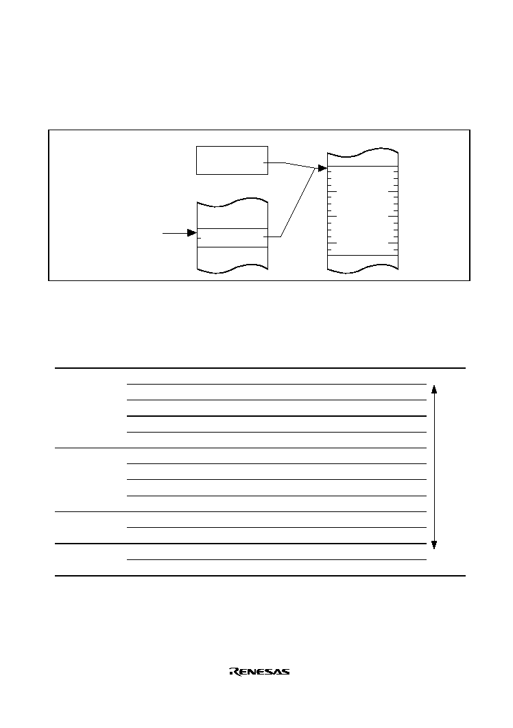
Rev. 2.0, 09/02, page 113 of 732
Through DTC activation, a register information start address is read from the vector table, then
register information placed in memory space is read from that register information start address.
Always designate register information start addresses in multiples of four.
DTBR
DTC vector table
DTC vector address
Transfer information
start address
(upper 16 bits)
Register
information
Memory space
Register information
start address
(lower 16 bits)
Figure 8.4 Correspondence between DTC Vector Address and Transfer Information
Table 8.1 Interrupt Sources, DTC Vector Addresses, and Corresponding DTEs
Activating
Source
Generator
Activating
Source
DTC Vector
Address
DTE Bit
Transfer
Source
Transfer
Destination
Priority
MTU (CH4)
TGIA_4
H'00000400
DTEA7
Arbitrary
*
Arbitrary
*
High
TGIB_4
H'00000402
DTEA6
Arbitrary
*
Arbitrary
*
TGIC_4
H'00000404
DTEA5
Arbitrary
*
Arbitrary
*
TGID_4
H'00000406
DTEA4
Arbitrary
*
Arbitrary
*
TCIV_4
H'00000408
DTEA3
Arbitrary
*
Arbitrary
*
MTU (CH3)
TGIA_3
H'0000040A
DTEA2
Arbitrary
*
Arbitrary
*
TGIB_3
H'0000040C
DTEA1
Arbitrary
*
Arbitrary
*
TGIC_3
H'0000040E
DTEA0
Arbitrary
*
Arbitrary
*
TGID_3
H'00000410
DTEB7
Arbitrary
*
Arbitrary
*
MTU (CH2)
TGIA_2
H'00000412
DTEB6
Arbitrary
*
Arbitrary
*
TGIB_2
H'00000414
DTEB5
Arbitrary
*
Arbitrary
*
MTU (CH1)
TGIA_1
H'00000416
DTEB4
Arbitrary
*
Arbitrary
*
TGIB_1
H'00000418
DTEB3
Arbitrary
*
Arbitrary
*
Low

Rev. 2.0, 09/02, page 114 of 732
Activating
Source
Generator
Activating
Source
DTC Vector
Address
DTE Bit
Transfer
Source
Transfer
Destination
Priority
MTU (CH0)
TGIA_0
H'0000041A
DTEB2
Arbitrary
*
Arbitrary
*
High
TGIB_0
H'0000041C
DTEB1
Arbitrary
*
Arbitrary
*
TGIC_0
H'0000041E
DTEB0
Arbitrary
*
Arbitrary
*
TGID_0
H'00000420
DTEC7
Arbitrary
*
Arbitrary
*
A/D converter
(CH0)
ADI0
H'00000422
DTEC6
ADDR0
Arbitrary
*
External pin
IRQ0
H'00000424
DTEC5
Arbitrary
*
Arbitrary
*
IRQ1
H'00000426
DTEC4
Arbitrary
*
Arbitrary
*
IRQ2
H'00000428
DTEC3
Arbitrary
*
Arbitrary
*
IRQ3
H'0000042A
DTEC2
Arbitrary
*
Arbitrary
*
IRQ4
H'0000042C
DTEC1
Arbitrary
*
Arbitrary
*
IRQ5
H'0000042E
DTEC0
Arbitrary
*
Arbitrary
*
IRQ6
H'00000430
DTED7
Arbitrary
*
Arbitrary
*
IRQ7
H'00000432
DTED6
Arbitrary
*
Arbitrary
*
CMT (CH0)
CMI0
H'00000434
DTED5
Arbitrary
*
Arbitrary
*
CMT (CH1)
CMI1
H'00000436
DTED4
Arbitrary
*
Arbitrary
*
RXI_0
H'00000438
DTED3
RDR_0
Arbitrary
*
SCI0
TXI_0
H'0000043A
DTED2
Arbitrary
*
TDR_0
RXI_1
H'0000043C
DTED1
RDR_1
Arbitrary
*
SCI1
TXI_1
H'0000043E
DTED0
Arbitrary
*
TDR_1
Reserved
--
H'00000440 to
H'00000443
--
--
--
A/D converter
(CH1)
ADI1
H'00000444
DTEE5
ADDR1
Arbitrary
*
Reserved
--
H'00000446
--
--
--
SCI2
RXI_2
H'00000448
DTEE3
RDR_2
Arbitrary
*
TXI_2
H'0000044A
DTEE2
Arbitrary
*
TDR_2
SCI3
RXI_3
H'0000044C
DTEE1
RDR_3
Arbitrary
*
TXI_3
H'0000044E
DTEE0
Arbitrary
*
TDR_3
Reserved
--
H'00000450 to
H'0000045F
--
--
--
Low

Rev. 2.0, 09/02, page 115 of 732
Activating
Source
Generator
Activating
Source
DTC Vector
Address
DTE Bit
Transfer
Source
Transfer
Destination
Priority
IIC
ICI
H'00000460
DTEG7
ICDR
(receive)
Arbitrary
*
(receive)
High
Arbitrary
*
(transmit)
ICDR
(transmit)
Reserved
--
H'00000462 to
H'0000049F
--
--
--
Software
Write to
DTCSR
H'0400+
DTVEC[7:0]
--
Arbitrary
*
Arbitrary
*
Low
Note:
*
External memory, memory-mapped external devices, on-chip memory, on-chip peripheral
modules (excluding DMAC and DTC)
8.3.3
DTC Operation
Register information is stored in an on-chip RAM. When activated, the DTC reads register
information in an on-chip RAM and transfers data. After the data transfer, it writes updated
register information back to the RAM.
Pre-storage of register information in the RAM makes it possible to transfer data over any required
number of channels. The transfer mode can be specified as normal, repeat, and block transfer
mode. Setting the CHNE bit to 1 makes it possible to perform a number of transfers with a single
activation source (chain transfer).
The 32-bit DTSAR designates the DTC transfer source address and the 32-bit DTDAR designates
the transfer destination address. After each transfer, DTSAR and DTDAR are independently
incremented, decremented, or left fixed depending on its register information.
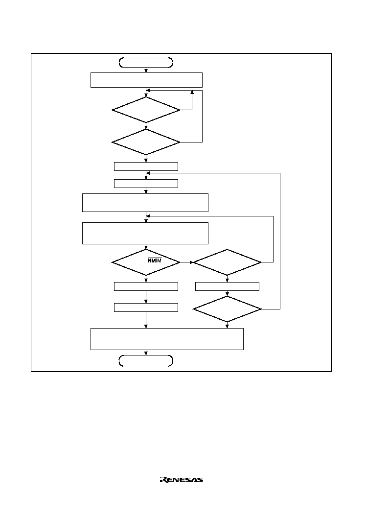
Rev. 2.0, 09/02, page 116 of 732
Yes
No
Yes
Yes
Yes
Yes
No
No
No
No
Start
Initial settings
DTMR, DTCR, DTIAR, DTSAR, DTDAR
Transfer request
generated?
NMIF = AE = 0?
DTC vector read
Transfer information read
DTCRA = DTCRA ≠ 1 (normal/block transfer mode)
DTCRAL = DTCRAL ≠ 1 (repeat mode)
DTSAR, DTDAR update
DTCRB = DTCRB ≠ 1 (block transfer mode)
Transfer (1 transfer unit)
Block
transfer mode and
DTCRB
0?
Transfer information write
NMI or address error
End
Transfer information write
CHNE = 0?
NMIF ∑
+ AE = 1?
When DISEL = 1 or DTCRA = 0 (normal/block transfer mode)
When DISEL = 1 (repeat transfer mode)
CPU interrupt request
Figure 8.5 DTC Operation Flowchart
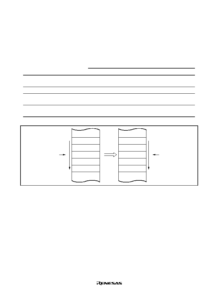
Rev. 2.0, 09/02, page 117 of 732
Normal Mode: Performs the transfer of one byte, one word, or one longword for each activation.
The total transfer count is 1 to 65536. Once the specified number of transfers have ended, a CPU
interrupt can be requested.
Table 8.2 Normal Mode Register Functions
Values Written Back upon a Transfer Information Write
Register
Function
When DTCRA is other than 1
When DTCRA is 1
DTMR
Operation mode
control
DTMR
DTMR
DTCRA
Transfer count
DTCRA ≠ 1
DTCRA ≠ 1 (= H'0000)
DTSAR
Transfer source
address
Increment/decrement/fixed
Increment/decrement/fixed
DTDAR
Transfer destination
address
Increment/decrement/fixed
Increment/decrement/fixed
Transfer
DTSAR
DTDAR
Figure 8.6 Memory Mapping in Normal Mode
Repeat Mode: Performs the transfer of one byte, one word, or one longword for each activation.
Either the transfer source or transfer destination is designated as the repeat area. Table 8.3 lists the
register information in repeat mode.
From 1 to 256 transfers can be specified. Once the specified number of transfers have ended, the
initial state of the transfer counter and the address register specified as the repeat area is restored,
and transfer is repeated. In repeat mode the transfer counter value does not reach H'00, and
therefore CPU interrupts cannot be requested when DISEL = 0.
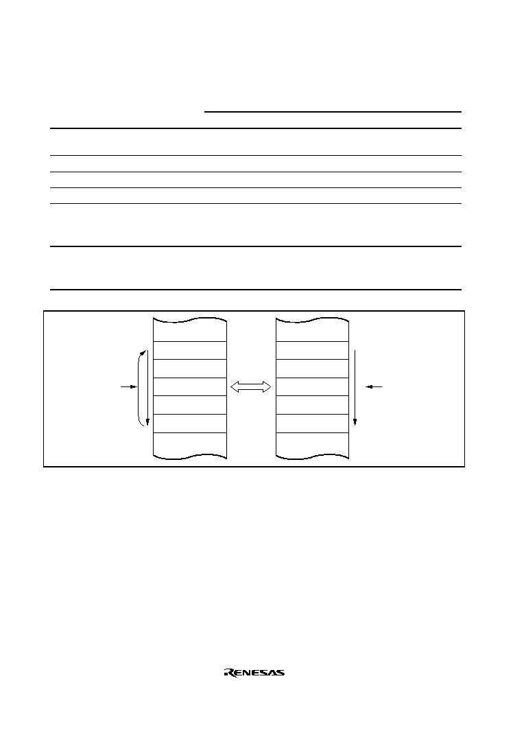
Rev. 2.0, 09/02, page 118 of 732
Table 8.3 Repeat Mode Register Functions
Values Written Back upon a Transfer Information Write
Register
Function
When DTCRA is other than 1
When DTCRA is 1
DTMR
Operation mode
control
DTMR
DTMR
DTCRAH
Transfer count save
DTCRAH
DTCRAH
DTCRAL
Transfer count
DTCRAL ≠ 1
DTCRAH
DTIAR
Initial address
(Not written back)
(Not written back)
DTSAR
Transfer source
address
Increment/decrement/fixed
(DTS = 0) Increment/
decrement/fixed
(DTS = 1) DTIAR
DTDAR
Transfer destination
address
Increment/decrement/fixed
(DTS = 0) DTIAR
(DTS = 1) Increment/
decrement/fixed
Transfer
DTSAR
or
DTDAR
DTDAR
or
DTSAR
Repeat area
Figure 8.7 Memory Mapping in Repeat Mode
Block Transfer Mode: Performs the transfer of one block for each one activation. Either the
transfer source or transfer destination is designated as the block area.
The block length is specified between 1 and 65536. When the transfer of one block ends, the
initial state of the block size counter and the address register specified as the block area is
restored. The other address register is then incremented, decremented, or left fixed.
From 1 to 65,536 transfers can be specified. Once the specified number of transfers have ended, a
CPU interrupt is requested.
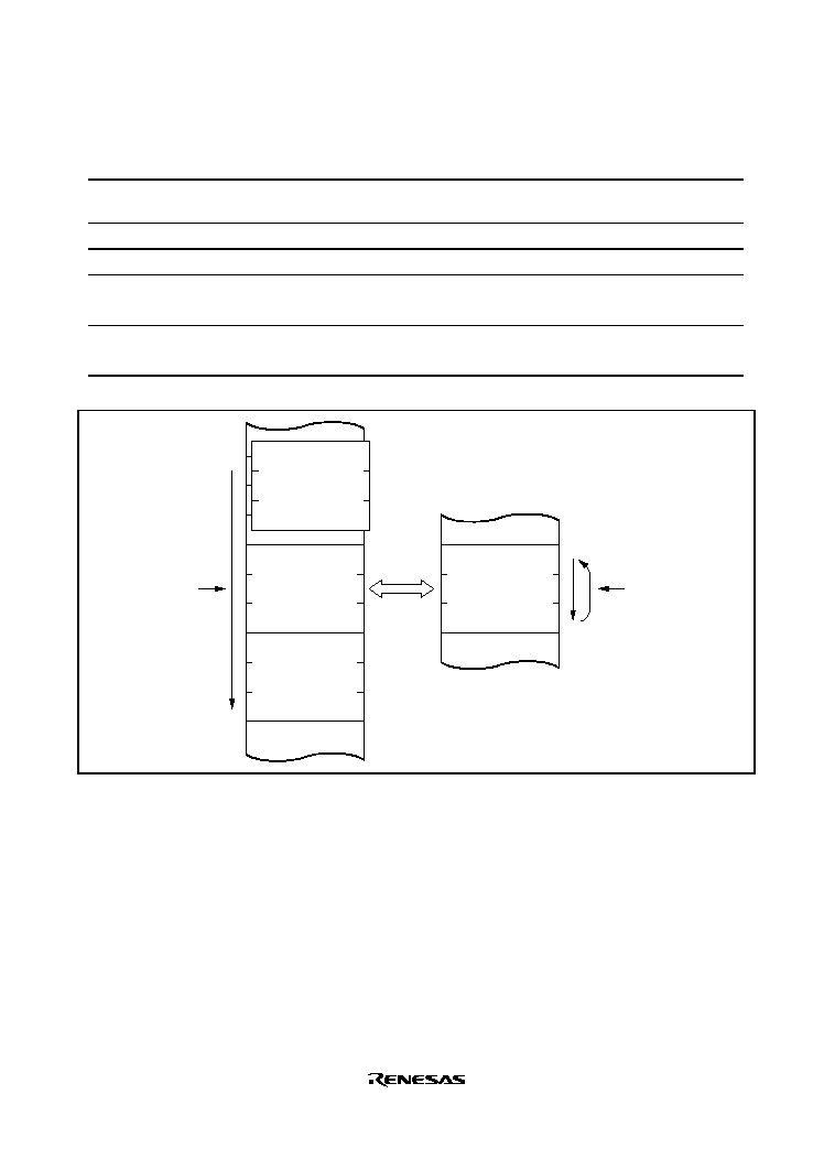
Rev. 2.0, 09/02, page 119 of 732
Table 8.4 Block Transfer Mode Register Functions
Register
Function
Values Written Back upon a Transfer Information Write
DTMR
Operation mode
control
DTMR
DTCRA
Transfer count
DTCRA ≠ 1
DTCRB
Block length
(Not written back)
DTSAR
Transfer source
address
(DTS = 0) Increment/ decrement/ fixed
(DTS = 1) DTSAR initial value
DTDAR
Transfer destination
address
(DTS = 0) DTDAR initial value
(DTS = 1) Increment/ decrement/ fixed
Transfer
DTSAR
or
DTDAR
DTDAR
or
DTSAR
Block area
∑
∑
∑
First block
Nth block
Figure 8.8 Memory Mapping in Block Transfer Mode
Chain Transfer: Setting the CHNE bit to 1 enables a number of data transfers to be performed
consecutively in a single activation source. DTSAR, DTDAR, DTMR, DTCRA, and DTCRB can
be set independently.
Figure 8.9 shows the chain transfer.
When activated, the DTC reads the register information start address stored at the vector address,
and then reads the first register information at that start address. After the data transfer, the CHNE
bit will be tested. When it has been set to 1, DTC reads next register information located in a
consecutive area and performs the data transfer. These sequences are repeated until the CHNE bit
is cleared to 0.
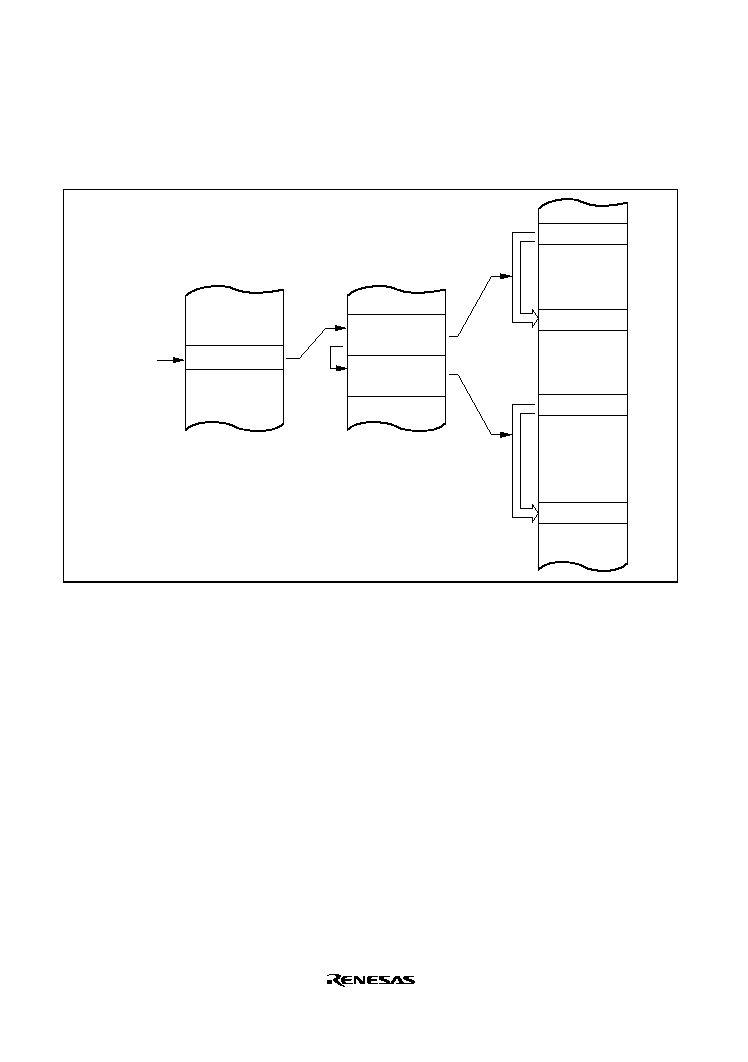
Rev. 2.0, 09/02, page 120 of 732
In the case of transfer with CHNE set to 1, an interrupt request to the CPU is not generated at the
end of the specified number of transfers or by setting of the DISEL bit to 1, and the interrupt
source flag for the activation source is not affected.
DTC vector
address
Source
Destination
Source
Destination
Register information
CHNE = 1
Register information
CHNE = 0
Register information
start address
Figure 8.9 Chain Transfer
8.3.4
Interrupt Source
An interrupt request is issued to the CPU when the DTC finishes the specified number of data
transfers, or a data transfer for which the DISEL bit was set to 1. In the case of interrupt
activation, the interrupt set as the activation source is generated. These interrupts to the CPU are
subject to CPU mask level and interrupt controller priority level control.
In the case of activation by software, a software activated data transfer end interrupt (SWDTEND)
is generated.
When the DISEL bit is 1 and one data transfer has ended, or the specified number of transfers
have ended, after data transfer ends, the SWDTE bit is held at 1 and an SWDTEND interrupt is
generated. The interrupt handling routine should clear the SWDTE bit to 0.
When the DTC is activated by software, an SWDTEND interrupt is not generated during a data
transfer wait or during data transfer even if the SWDTE bit is set to 1.
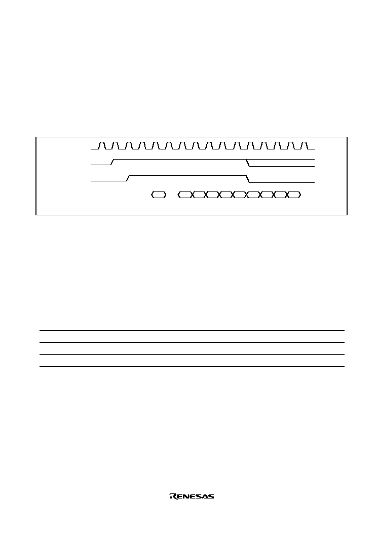
Rev. 2.0, 09/02, page 121 of 732
Note:
When the DTCR contains a value equal to or greater than 2, the SWDTE bit is
automatically cleared to 0. When the DTCR is set to 1, the SWDTE bit is again set to 1.
8.3.5
Operation Timing
When register information is located in on-chip RAM, each mode requires 4 cycles for transfer
information reads, and 3 cycles for writes.
Activating
source
Address
Vector
read
Transfer information
read
Data
transfer
R
W
Transfer
information write
DTC
request
Figure 8.10 DTC Operation Timing Example (Normal Mode)
8.3.6
DTC Execution State Counts
Table 8.5 shows the execution state for one DTC data transfer. Furthermore, table 8.6 shows the
state counts needed for execution state.
Table 8.5 Execution State of DTC
Mode
Vector Read I
Register
Information
Read/Write J
Data Read K
Data Write L
Internal
Operation M
Normal
1
7
1
1
1
Repeat
1
7
1
1
1
Block transfer
1
7
N
N
1
N: block size (default set values of DTCRB)

Rev. 2.0, 09/02, page 122 of 732
Table 8.6 State Counts Needed for Execution State
Access Objective
On-chip
RAM
On-chip
ROM
Internal I/O
Register
External Device
Bus width
32
32
8 or 16
8
16
32
Access state
1
1
2
*
1
3
*
2
2
2
2
Vector read
S
I
--
1
--
--
4
2
2
Register information
read/write
S
J
1
1
--
--
8
4
2
Byte data read
S
K
1
1
2
3
2
2
2
Word data read
S
K
1
1
2
3
4
2
2
Long word data read
S
K
1
1
4
6
8
4
2
Byte data write
S
L
1
1
2
3
2
2
2
Word data write
S
L
1
1
2
3
4
2
2
Longword data write
S
L
1
1
4
6
8
4
2
Execution
state
Internal operation
S
M
1
Notes: 1. Two state access module : port, INT, CMT, SCI, etc.
2. Three state access module : WDT, UBC, etc.
The execution state count is calculated using the following formula.
indicates the number of
transfers by one activating source (count + 1 when CHNE bit is set to 1).
Execution state count = I ∑ S
I
+
(J ∑ S
J
+ K ∑ S
K
+ L ∑ S
L
) + M ∑ S
M
8.4
Procedures for Using DTC
8.4.1
Activation by Interrupt
The procedure for using the DTC with interrupt activation is as follows:
1. Set the DTMR, DTCRA, DTSAR, DTDAR, DTCRB, and DTIAR register information in
memory space.
2. Specify the register information start address with DTBR and the DTC vector table.
3. Set the corresponding DTER bit to 1.
4. The DTC is activated when an interrupt source occurs.
5. When interrupt requests are not made to the CPU, the interrupt source is cleared, but the DTER
is not. When interrupts are requested, the interrupt source is not cleared, but the DTER is.
6. Interrupt sources are cleared within the CPU interrupt routine. When doing continuous DTC
data transfers, set the DTER to 1.

Rev. 2.0, 09/02, page 123 of 732
8.4.2
Activation by Software
The procedure for using the DTC with software activation is as follows:
1. Set the DTMR, DTCRA, DTSAR, DTDAR, DTCRB, and DTIAR register information in
memory space.
2. Set the start address of the register information in the DTBR register and the DTC vector
address.
3. Check that the SWDTE bit is 0.
4. Write 1 to SWDTE bit and the vector number to DTVEC.
5. Check the vector number written to DTVEC.
6. After the end of one data transfer, if the DISEL bit is 0 and a CPU interrupt is not requested,
the SWDTE bit is cleared to 0. If the DTC is to continue transferring data, set the SWDTE bit
to 1. When the DISEL bit is 1, or after the specified number of data transfers have ended, the
SWDTE bit is held at 1 and a CPU interrupt is requested.
7. The SWDTE bit is cleared to 0 within the CPU interrupt routine. For continuous DTC data
transfer, set the SWDTE bit to 1 after confirming that its current value is 0. Then write the
vector number to DTVEC for continuous DTC transfer.
8.4.3
DTC Use Example
The following is a DTC use example of a 128-byte data reception by the SCI:
1. The settings are: DTMR source address fixed (SM1 = SM0 = 0), destination address
incremented (DM1 = 1, DM0 = 0), normal mode (MD1 = MD0 = 0), byte size (SZ1 = SZ0 =
0), one transfer per activating source (CHNE = 0), and a CPU interrupt request after the
designated number of data transfers (DISEL = 0). DTS bit can be set to any value. 128
(H'0080) is set in DTCRA, the RDR address of the SCI is set in DTSAR, and the start address
of the RAM storing the receive data is set in DTDAR. DTCRB can be set to any value.
2. Set the register information start address with DTBR and the DTC vector table.
3. Set the corresponding DTER bit to 1.
4. Set the SCI to the appropriate receive mode. Set the RIE bit in SCR to 1 to enable the
reception complete (RXI) interrupt. Since the generation of a receive error during the SCI
reception operation will disable subsequent reception, the CPU should be enabled to accept
receive error interrupts.
5. Each time reception of one byte of data ends on the SCI, the RDRF flag in SSR is set to 1, an
RXI interrupt is generated, and the DTC is activated. The receive data is transferred from RDR
to RAM by the DTC. DTDAR is incremented and DTCRA is decremented. The RDRF flag is
automatically cleared to 0.
6. When DTCRA is 0 after the 128 data transfers have ended, the RDRF flag is held at 1, the
corresponding bit in DTER is cleared to 0, and an RXI interrupt request is sent to the CPU.
The interrupt handling routine should perform completion processing.

Rev. 2.0, 09/02, page 124 of 732
8.5
Cautions on Use
8.5.1
Prohibition against DMAC/DTC Register Access by DTC
DMAC and DTC register access by the DMAC is prohibited.
8.5.2
Module Standby Mode Setting
DTC operation can be disabled or enabled using the module standby control register. The initial
setting is for DTC operation to be halted. Register access is enabled by clearing module standby
mode.
When the MSTP24 and MSTP25 bits in MSTCR1 are set to 1, the DTC clock is halted and the
DTC enters module standby mode. The MSTP24 and MSTP25 bit cannot be set to 1 during
activation of the DTC.
In addition, when the module standby mode is entered, clear all the DTER bits to 0.
For details, refer to section 24, Power-Down Modes.
8.5.3
On-Chip RAM
The DTMR, DTSAR, DTDAR, DTCRA,DTCRB and DTIAR registers are all located in on-chip
RAM. When the DTC is used, the RAME bit in SYSCR must not be cleared to 0.

BSC1001A_010020020700
Rev. 2.0, 09/02, page 125 of 732
Section 9 Bus State Controller (BSC)
The bus state controller (BSC) divides up the address spaces and outputs control signals for
various types of memory. This enables memories like SRAM and ROM to be connected directly
to the chip without external circuitry.
9.1
Features
The BSC has the following features:
∑
Address space is divided into four spaces
A maximum linear 2 Mbytes for on-chip ROM enabled mode, and a maximum 4-Mbyte for
on-chip ROM disabled mode, for address space CS0
A maximum linear 4-Mbyte for address space CS1, CS2, CS3
Bus width (8, 16, or 32 bits) can be selected for each space
Wait states can be inserted by software for each space
Wait state insertion with
WAIT pin in external memory space access
Outputs control signals for each space according to the type of memory connected
∑
On-chip ROM and RAM interfaces
On-chip ROM and RAM access of 32 bits in 1 state
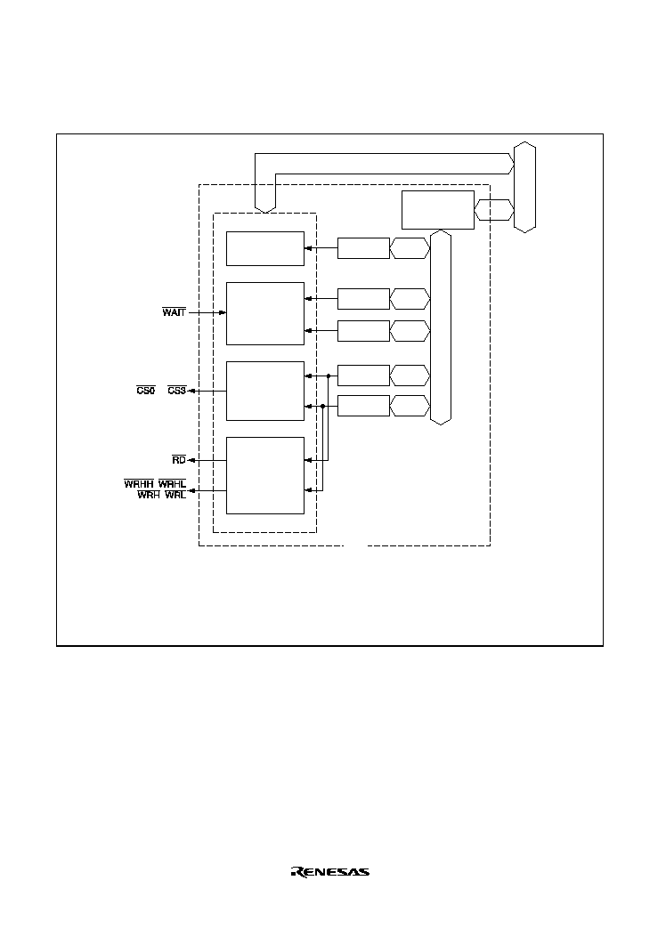
Rev. 2.0, 09/02, page 126 of 732
Figure 9.1 shows the BSC block diagram.
RAMER
WCR1
BCR1
BCR2
WCR2
Internal bus
Module bus
Bus interface
On-chip memory
control unit
Memory control
unit
Wait control
unit
Area control
unit
,
,
to
BSC
WCR1:
Wait control register 1
WCR2:
BCR1:
Bus control register 1
BCR2:
Bus control register 2
RAMER: RAM emulation register
Wait control register 2
Note: Refer to section 19, Flash Memory (F-ZTAT Version), for RAMER.
Figure 9.1 BSC Block Diagram

Rev. 2.0, 09/02, page 127 of 732
9.2
Pin Configuration
Table 9.1 shows the bus state controller pin configuration.
Table 9.1 Pin Configuration
Name
Abbr.
I/O
Description
Address bus
A21 to A0
Output Address output (Address bus A21 to A18 pins are
disabled and I/O port function is enabled after
power-on-reset.)
Data bus
D31 to D0
I/O
32-bit data bus
Chip select
CS0
to
CS3
Output Chip select signal indicating the area being
accessed
Read
RD
Output Strobe that indicates the read cycle
WRHH
Output Strobe that indicates a write cycle to the first byte
(D31 to D24)
WRHL
Output Strobe that indicates a write cycle to the second byte
(D23 to D16)
WRH
Output Strobe that indicates a write cycle to the third byte
(D15 to D8)
Write
WRL
Output Strobe that indicates a write cycle to the fourth byte
(D7 to D0)
Wait
WAIT
Input
Wait state request signal
Bus request
BREQ
Input
Bus request input
Bus acknowledge
BACK
Output Bus use enable output
9.3
Register Descriptions
The BSC has five registers. For details on these register addresses and register states in each
processing states, refer to section 25, List of Registers.
These registers are used to control wait states, bus width, and interfaces with memories like ROM
and SRAM. All registers are 16 bits.
∑
Bus control register 1 (BCR1)
∑
Bus control register 2 (BCR2)
∑
Wait control register 1 (WCR1)
∑
Wait control register 2 (WCR2)
∑
RAM emulation register (RAMER)

Rev. 2.0, 09/02, page 128 of 732
9.4
Address Map
Figure 9.2 shows the address format used by this LSI.
Output address:
Output from the address pins
CS space selection:
Decoded, outputs
to
when A31 to A24 = 00000000
Space selection:
Not output externally; used to select the type of space
On-chip ROM space or CS space when 00000000 (H'00)
Reserved (do not access) when 00000001 to 11111110 (H'01 to H'FE)
On-chip peripheral module space or on-chip RAM space when 11111111 (H'FF)
A31 to A24
A23, A22
A21
A0
Figure 9.2 Address Format
This chip uses 32-bit addresses:
∑
Bits A31 to A24 are used to select the type of space and are not output externally.
∑
Bits A23 and A22 are decoded and output as chip select signals (
CS3 to CS0) for the
corresponding areas when bits A31 to A24 are 00000000.
∑
A21 to A0 are output externally.
Table 9.2 shows the address map.
Table 9.2 Address Map
On-chip ROM enabled mode
Address
Space
Memory
Size
Bus Width
H'00000000 to H'0003FFFF
On-chip ROM
On-chip ROM
256 kbytes
32 bits
H'00040000 to H'001FFFFF
Reserved
Reserved
H'00200000 to H'003FFFFF
CS0 space
External space
2 Mbytes
8/16/32 bits
*
1
H'00400000 to H'007FFFFF
CS1 space
External space
4 Mbytes
8/16/32 bits
*
1
H'00800000 to H'00BFFFFF
CS2 space
External space
4 Mbytes
8/16/32 bits
*
1
H'00C00000 to H'00FFFFFF
CS3 space
External space
4 Mbytes
8/16/32 bits
*
1
H'01000000 to H'FFFF7FFF
Reserved
Reserved
H'FFFF8000 to H'FFFFBFFF
On-chip peripheral
module
On-chip peripheral
module
16 kbytes
8/16 bits
H'FFFFC000 to H'FFFFDFFF
Reserved
Reserved
H'FFFFE000 to H'FFFFFFFF
On-chip RAM
On-chip RAM
8 kbytes
32 bits

Rev. 2.0, 09/02, page 129 of 732
On-chip ROM disabled mode
Address
Space
Memory
Size
Bus Width
H'00000000 to H'003FFFFF
CS0 space
External space
4 Mbytes
8/16/32 bits
*
2
H'00400000 to H'007FFFFF
CS1 space
External space
4 Mbytes
8/16/32 bits
*
1
H'00800000 to H'00BFFFFF
CS2 space
External space
4 Mbytes
8/16/32 bits
*
1
H'00C00000 to H'00FFFFFF
CS3 space
External space
4 Mbytes
8/16/32 bits
*
1
H'01000000 to H'FFFF7FFF
Reserved
Reserved
H'FFFF8000 to H'FFFFBFFF
On-chip peripheral
module
On-chip peripheral
module
16 kbytes
8/16 bits
H'FFFFC000 to H'FFFFDFFF
Reserved
Reserved
H'FFFFE000 to H'FFFFFFFF
On-chip RAM
On-chip RAM
8 kbytes
32 bits
Notes: Do not access reserved spaces. Operation cannot be guaranteed if they are accessed.
Spaces other than on-chip ROM, on-chip RAM, and on-chip peripheral modules cannot be
used in single-chip mode.
1. Selected by setting the on-chip register.
2. Selected by the mode pin: 8 or 16 bits in SH7144 (112 pins)
16 or 32 bits in SH7145 (144 pins)

Rev. 2.0, 09/02, page 130 of 732
9.5
Description of Registers
9.5.1
Bus Control Register 1 (BCR1)
BCR1 is a 16-bit readable/writable register that enables access to the MTU control registers and
specifies the bus size of each CS space. When using the SH7144, specify the bus size as word (16-
bit) or smaller size.
Write bits 7 to 0 of BCR1 during the initialization stage after a power-on reset, and do not change
the values thereafter. In on-chip ROM enabled mode, do not access any of each CS space until
completion of register initialization. In on-chip ROM disabled mode, do not access CS spaces
other than CS0 until completion of register initialization.
Bit
Bit Name Initial Value
R/W
Description
15
0
R
Reserved
This bit is always read as 0 and should always be
written with 0.
14
1
R
Reserved
This bit is always read as 1 and should always be
written with 1.
13
MTURWE 1
R/W
MTU Read/Write Enable
This bit enables MTU control register access. For
details, refer to section 11, Multi-Function Timer
Pulse Unit (MTU).
0: MTU control register access is disabled
1: MTU control register access is enabled
12 to 8
All 0
R
Reserved
These bits are always read as 0 and should always
be written with 0.
7
A3LG
0
R/W
CS3 space longword
This bit specifies the CS3 space bus size. This bit is
valid only for the SH7145.
This bit is reserved in SH7144. This bit is always read
as 0 and should always be written with 0.
0: Depends on the value set with the A3SZ bit in this
register.
1: Longword (32 bits)

Rev. 2.0, 09/02, page 131 of 732
Bit
Bit Name Initial Value
R/W
Description
6
A2LG
0
R/W
CS2 space longword
This bit specifies the CS2 space bus size. This bit is
valid only for the SH7145.
This bit is reserved in SH7144. This bit is always read
as 0 and should always be written with 0.
0: Depends on the value set with the A2SZ bit in this
register.
1: Longword (32 bits)
5
A1LG
0
R/W
CS1 space longword
This bit specifies the CS1 space bus size. This bit is
valid only for the SH7145.
This bit is reserved in SH7144. This bit is always read
as 0 and should always be written with 0.
0: Depends on the value set with the A1SZ bit in this
register.
1: Longword (32 bits)
4
A0LG
0
R/W
CS0 space longword
This bit specifies the CS0 space bus size. This bit is
valid only for the SH7145.
This bit is reserved in SH7144. This bit is always read
as 0 and should always be written with 0.
0: Depends on the value set with the A0SZ bit in this
register.
1: Longword (32 bits)
Note:
A0LG is valid only in on-chip ROM enabled
mode. The CS0 space bus size is specified
with the mode pin in on-chip ROM disabled
mode.
3
A3SZ
1
R/W
CS3 space size
This bit specifies the CS3 space bus size in A3LG= 0.
0: Byte (8 bits)
1: Word (16 bits)
Note:
In A3LG= 1, This bit is ignored and the CS3
bus size is longword (32bits).

Rev. 2.0, 09/02, page 132 of 732
Bit
Bit Name Initial Value
R/W
Description
2
A2SZ
1
R/W
CS2 space size
This bit specifies the CS2 space bus size in A2LG= 0.
0: Byte (8 bits)
1: Word (16 bits)
Note:
In A2LG= 1, This bit is ignored and the CS2
bus size is longword (32bits).
1
A1SZ
1
R/W
CS1 space size
This bit specifies the CS1 space bus size in A1LG= 0.
0: Byte (8 bits)
1: Word (16 bits)
Note:
In A1LG= 1, This bit is ignored and the CS1
bus size is longword (32bits).
0
A0SZ
1
R/W
CS0 space size
This bit specifies the CS0 space bus size in A0LG= 0.
0: Byte (8 bits)
1: Word (16 bits)
Note:
This bit is valid only in on-chip ROM enabled
mode. The CS0 space bus size is specified
with the mode pin in on-chip ROM disabled
mode. Even in on-chip ROM enabled mode,
this bit is ignored in A0LG= 1, and the CS0
space bus size is longword (32 bits).
9.5.2
Bus Control Register 2 (BCR2)
BCR2 is a 16-bit readable/writable register that specifies the number of idle cycles and
CS signal
assert extension of each CS space.
Bit
Bit Name Initial Value R/W
Description
15
14
IW31
IW30
1
1
R/W
R/W
Idle cycles in CS3 space cycles
These bits insert idle cycles when the write cycle to the
CS3 space comes after read access to the CS3 space, or
when continuous access is made to different CS spaces
after read access to the CS3 space.
00: No idle cycle inserted after access to the CS3 space
01: One idle cycle inserted after access to the CS3 space
10: Two idle cycles inserted after access to the CS3 space
11: Three idle cycles inserted after access to the CS3
space

Rev. 2.0, 09/02, page 133 of 732
Bit
Bit Name Initial Value R/W
Description
13
12
IW21
IW20
1
1
R/W
R/W
Idle cycles in CS2 space cycles
These bits insert idle cycles when the write cycle to the
CS2 space comes after read access to the CS2 space, or
when continuous access is made to different CS spaces
after read access to the CS2 space.
00: No idle cycle inserted after access to the CS2 space
01: One idle cycle inserted after access to the CS2 space
10: Two idle cycles inserted after access to the CS2 space
11: Three idle cycles inserted after access to the CS2
space
11
10
IW11
IW10
1
1
R/W
R/W
Idle cycles in CS1 space cycles
These bits insert idle cycles when the write cycle to the
CS1 space comes after read access to the CS1 space, or
when continuous access is made to different CS spaces
after read access to the CS1 space.
00: No idle cycle inserted after access to the CS1 space
01: One idle cycle inserted after access to the CS1 space
10: Two idle cycles inserted after access to the CS1 space
11: Three idle cycles inserted after access to the CS1
space
9
8
IW01
IW00
1
1
R/W
R/W
Idle cycles in CS0 space cycles
These bits insert idle cycles when the write cycle to the
CS0 space comes after read access to the CS0 space, or
when continuous access is made to different CS spaces
after read access to the CS0 space.
00: No idle cycle inserted after access to the CS0 space
01: One idle cycle inserted after access to the CS0 space
10: Two idle cycles inserted after access to the CS0 space
11: Three idle cycles inserted after access to the CS0
space

Rev. 2.0, 09/02, page 134 of 732
Bit
Bit Name Initial Value R/W
Description
7
CW3
1
R/W
Idle cycles at continuous access to CS3 space
This bit inserts an idle cycle and negates the
CS
3 signal to
make the bus cycle end obvious when accessing the CS3
space continuously.
0: No idle cycle inserted at continuous access to the CS3
space.
1: One idle cycle inserted at continuous access to the CS3
space.
When the write cycle follows the read cycle, the larger of
the value specified with IW and that specified with CW is
used as the idle cycles to be inserted.
6
CW2
1
R/W
Idle cycles at continuous access to CS2 space
This bit inserts an idle cycle and negates the
CS
2 signal to
make the bus cycle end obvious when accessing the CS2
space continuously.
0: No idle cycle inserted at continuous access to the CS2
space.
1: One idle cycle inserted at continuous access to the CS2
space.
When the write cycle follows the read cycle, the larger of
the value specified with IW and that specified with CW is
used as the idle cycles to be inserted.
5
CW1
1
R/W
Idle cycles at continuous access to CS1 space
This bit inserts an idle cycle and negates the
CS
1 signal to
make the bus cycle end obvious when accessing the CS1
space continuously.
0: No idle cycle inserted at continuous access to the CS1
space.
1: One idle cycle inserted at continuous access to the CS1
space.
When the write cycle follows the read cycle, the larger of
the value specified with IW and that specified with CW is
used as the idle cycles to be inserted.

Rev. 2.0, 09/02, page 135 of 732
Bit
Bit Name Initial Value R/W
Description
4
CW0
1
R/W
Idle cycles at continuous access to CS0 space
This bit inserts an idle cycle and negates the
CS
0 signal to
make the bus cycle end obvious when accessing the CS0
space continuously.
0: No idle cycle inserted at continuous access to the CS0
space.
1: One idle cycle inserted at continuous access to the CS0
space.
When the write cycle follows the read cycle, the larger of
the value specified with IW and that specified with CW is
used as the idle cycles to be inserted.
3
SW3
1
R/W
CS
assert period extension for CS3 space
This bit inserts a cycle to prevent the assert period of
RD
and
WRx
from extending the assert period of
CS
3.
0: No cycle inserted for
CS
assert period.
1:
CS
assert extension (each one cycle inserted before and
after the bus cycle).
2
SW2
1
R/W
CS
assert period extension for CS2 space
This bit inserts a cycle to prevent the assert period of
RD
and
WRx
from extending the assert period of
CS
2.
0: No cycle inserted for
CS
assert period.
1:
CS
assert extension (each one cycle inserted before and
after the bus cycle).
1
SW1
1
R/W
CS
assert period extension for CS1 space
This bit inserts a cycle to prevent the assert period of
RD
and
WRx
from extending the assert period of
CS
1.
0: No cycle inserted for
CS
assert period.
1:
CS
assert extension (each one cycle inserted before and
after the bus cycle).
0
SW0
1
R/W
CS
assert period extension for CS0 space
This bit inserts a cycle to prevent the assert period of
RD
and
WRx
from extending the assert period of
CS
0.
0: No cycle inserted for
CS
assert period.
1:
CS
assert extension (each one cycle inserted before and
after the bus cycle).

Rev. 2.0, 09/02, page 136 of 732
9.5.3
Wait Control Register 1 (WCR1)
WCR1 is a 16-bit readable/writable register that specifies the number of wait cycles for each CS
space.
Bit
Bit Name
Initial Value
R/W
Description
15
14
13
12
W33
W32
W31
W30
1
1
1
1
R/W
R/W
R/W
R/W
CS3 Space Wait
Specification
These bits specify the number of waits for CS3 space
access.
0000: No wait (external wait input disabled)
0001: One wait (external wait input enabled)
.
.
.
1111: 15 waits (external wait input enabled)
11
10
9
8
W23
W22
W21
W20
1
1
1
1
R/W
R/W
R/W
R/W
CS2 Space Wait
Specification
These bits specify the number of waits for CS2 space
access.
0000: No wait (external wait input disabled)
0001: One wait (external wait input enabled)
.
.
.
1111: 15 waits (external wait input enabled)
7
6
5
4
W13
W12
W11
W10
1
1
1
1
R/W
R/W
R/W
R/W
CS1 Space Wait
Specification
These bits specify the number of waits for CS1 space
access.
0000: No wait (external wait input disabled)
0001: One wait (external wait input enabled)
.
.
.
1111: 15 waits (external wait input enabled)
3
2
1
0
W03
W02
W01
W00
1
1
1
1
R/W
R/W
R/W
R/W
CS0 Space Wait
Specification
These bits specify the number of waits for CS0 space
access.
0000: No wait (external wait input disabled)
0001: One wait (external wait input enabled)
.
.
.
1111: 15 waits (external wait input enabled)

Rev. 2.0, 09/02, page 137 of 732
9.5.4
Wait Control Register 2 (WCR2)
WCR2 is a 16-bit readable/writable register that specifies the number of access cycles to the CS
space in DMA single address mode transfer.
Do not perform DMA single address transfer before setting WCR2.
Bit
Bit Name Initial Value
R/W
Description
15 to 4
All 0
R
Reserved
These bits are always read as 0 and should always
be written with 0.
3
2
1
0
DSW3
DSW2
DSW1
DSW0
1
1
1
1
R/W
R/W
R/W
R/W
Number of wait cycles for access to CS space in
DMA single address mode
These bits specify the number of wait cycles (0 to 15)
for access to the CS space in DMA single address
mode. These bits are independent of the W bit in
WCR1.
0000: No wait (external wait insertion disabled)
0001: One wait (external wait insertion enabled)
:
1111: 15 waits (external waits insertion enabled)
9.5.5
RAM Emulation Register (RAMER)
The RAM emulation register (RAMER) is a 16-bit readable/writable register that selects the RAM
area to be used when emulating realtime programming of flash memory. For details, refer to
section 19.5.5, RAM Emulation Register (RAMER).
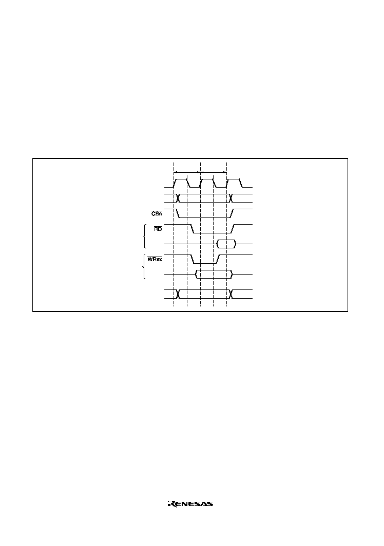
Rev. 2.0, 09/02, page 138 of 732
9.6
Accessing External Space
A strobe signal is output in external space accesses to provide primarily for SRAM or ROM direct
connections.
9.6.1
Basic Timing
External access bus cycles are performed in 2 states. Figure 9.3 shows the basic timing of external
space access.
Write
Data
DACK
Data
Address
CK
Read
T1
T2
Figure 9.3 Basic Timing of External Space Access
During a read, irrespective of operand size, all bits in the data bus width for the access space
(address) accessed by
RD signal are fetched by the LSI.
During a write, the
WRHH (bits 31 to 24) , the WRHL (bits 23 to 16) , the WRH (bits 15 to 8),
and the
WRL (bits 7 to 0) signal indicate the byte location to be written.
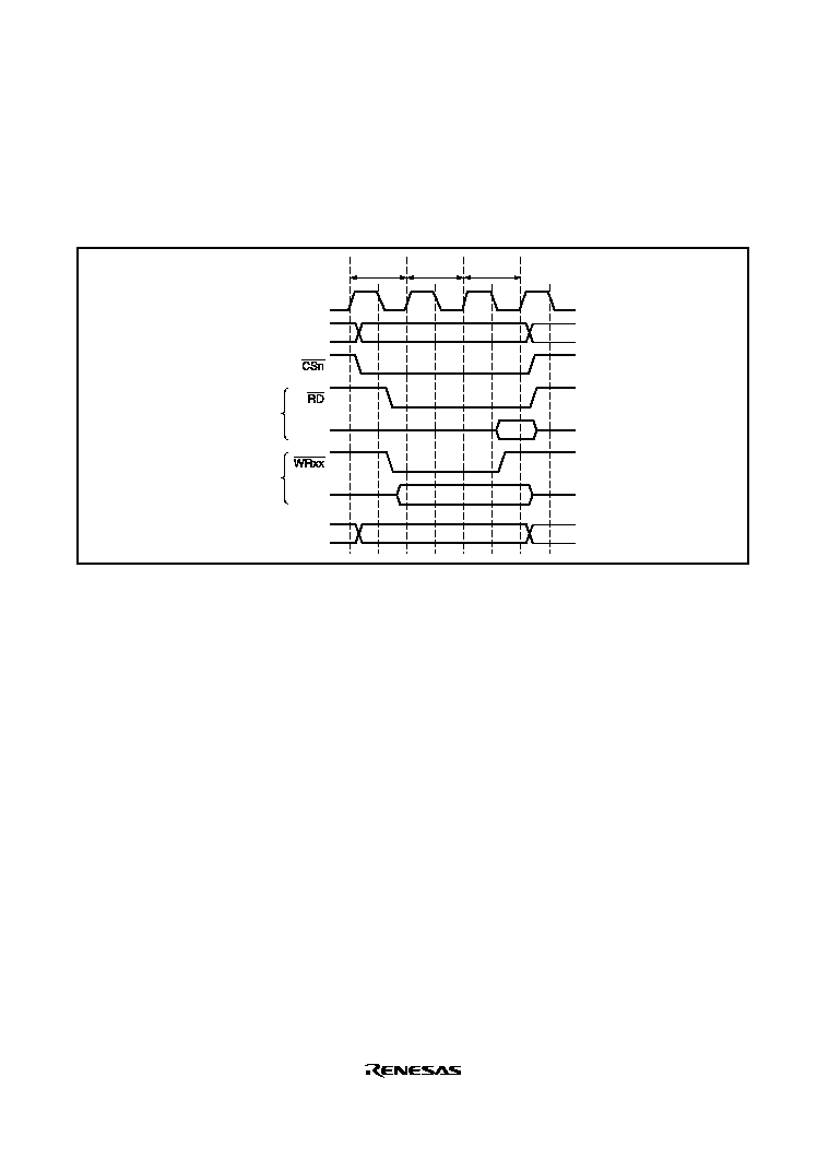
Rev. 2.0, 09/02, page 139 of 732
9.6.2
Wait State Control
The number of wait states inserted into external space access states can be controlled using the
WCR settings. The specified number of Tw cycles are inserted as software cycles at the timing
shown in figure 9.4.
Write
Data
DACK
Data
Address
CK
Read
T1
Tw
T2
Figure 9.4 Wait State Timing of External Space Access (Software Wait Only)
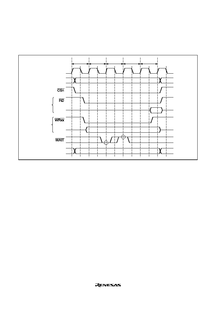
Rev. 2.0, 09/02, page 140 of 732
When the wait is specified by software using WCR, the wait input
WAIT signal from outside is
sampled. Figure 9.5 shows the
WAIT signal sampling. The WAIT signal is sampled at the clock
rise one cycle before the clock rise when the Tw state shifts to the T2 state.
Write
Data
Data
DACK
Address
CK
Read
T1
Tw
Tw
Two
T2
Figure 9.5 Wait State Timing of External Space Access
(Two Software Wait States
+
+
+
+
WAIT
WAIT
WAIT
WAIT Signal Wait State)
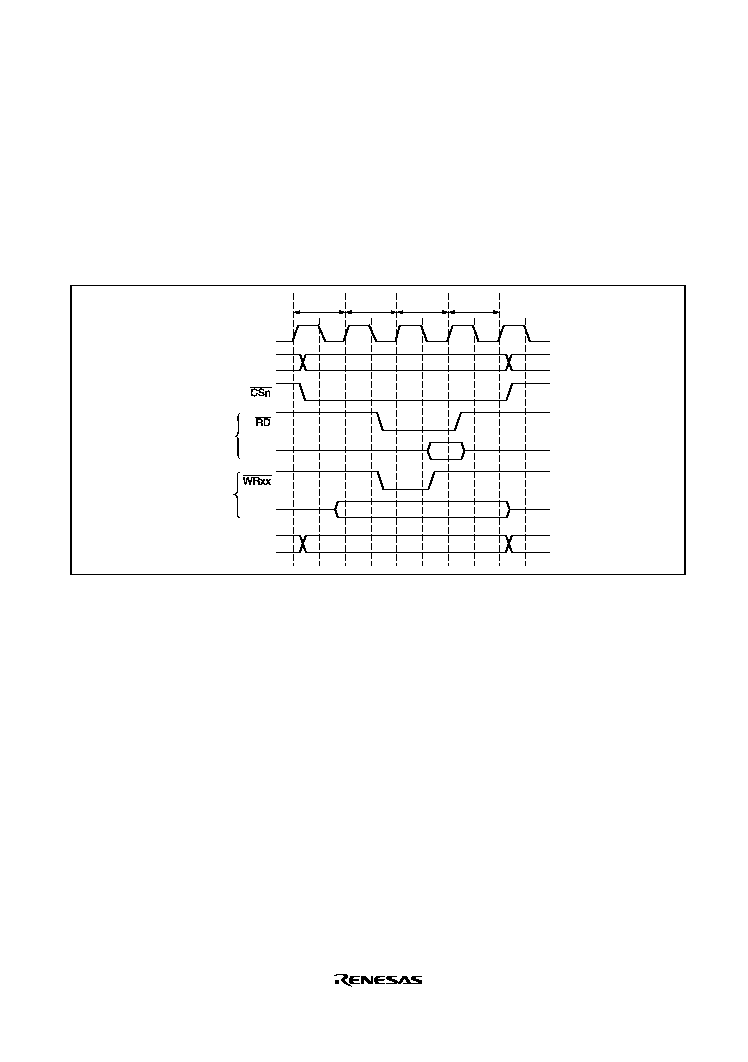
Rev. 2.0, 09/02, page 141 of 732
9.6.3
CS
CS
CS
CS Assert Period Extension
Idle cycles can be inserted to prevent extension of the
RD or WRxx signal assert period beyond
the length of the
CSn signal assert period by setting the SW3 to SW0 bits of BCR2. This allows
for flexible interfaces with external circuitry. The timing is shown in figure 9.6. Th and Tf cycles
are added respectively before and after the normal cycle. Only
CSn is asserted in these cycles; RD
and
WRxx signals are not. Further, data is extended up to the Tf cycle, which is effective for gate
arrays and the like, which have slower write operations.
Write
Data
Data
Address
DACK
CK
Read
Th
T1
T2
Tf
Figure 9.6
CS
CS
CS
CS Assert Period Extension Function

Rev. 2.0, 09/02, page 142 of 732
9.7
Waits between Access Cycles
When a read from a slow device is completed, data buffers may not go off in time, causing
conflict with the next access data. If there is a data conflict during memory access, the problem
can be solved by inserting a wait in the access cycle.
To enable detection of bus cycle starts, waits can be inserted between access cycles during
continuous accesses of the same CS space by negating the
CSn signal once.
9.7.1
Prevention of Data Bus Conflicts
Wait cycles are inserted in the following cases so that the number of idle cycles specified with the
IW31 to IW00 bits are inserted:
∑
The write cycle to the same CS space continues after the cycle read
∑
The continuous access is made to the different CS space after the read access
If there are idle cycles between the access cycles, the number of wait cycles is inserted that is
obtained by subtracting the existing idle cycles from the number of idle cycles specified.
Figure 9.7 shows the example of idle cycle insertion. In this example, when one idle cycle
insertion is specified between CSn space cycles, the specified one idle cycle is inserted when the
write access is performed to the CSm space immediately after the read cycle of the CSn space.
Rev. 2.0, 09/02, page 143 of 732
T1
T2
T1
T2
CK
Address
Data
CSn space read
Idle cycles
CSm space write
Tidle
Figure 9.7 Example of Idle Cycle Insertion
Bits IW31 and IW30 in BCR2 specify the number of idle cycles inserted in the case of a write
cycle to CS3 space or an access to different space after CS3 space read.
Bits IW21 and IW20 specify the number of idle cycles inserted for a CS2 space, bits IW11 and
IW10 specify for a CS1 space, and bits IW01 and IW00 specify for a CS0 space, respectively.
9.7.2
Simplification of Bus Cycle Start Detection
For consecutive accesses to the same CS space, waits are inserted to provide the number of idle
cycles designated by bits CW3 to CW0 in BCR2. However, in the case of a write cycle after a
read, the number of idle cycles inserted will be the larger of the two values designated by the IW
and CW bits. When idle cycles already exist between access cycles, waits are not inserted.
Figure 9.8 shows an example. A continuous access idle is specified for CSn space, and CSn space
is consecutively write-accessed.
Rev. 2.0, 09/02, page 144 of 732
Data
CSn space access
Idle cycle
CSn space access
Address
CK
T1
T2
Tidle
T1
T2
Figure 9.8 Example of Idle Cycle Insertion at Same Space Consecutive Access
9.8
Bus Arbitration
This LSI has a bus arbitration function that, when a bus release request is received from an
external device, releases the bus to that device. It also has four internal bus masters, the CPU,
DMAC, DTC, and AUD. The priority for arbitrate the bus mastership between these bus masters
is:
Bus request from external device > AUD > DTC > DMAC > CPU
AUD does not acquire the bus mastership during DTC or DMAC burst transfer; it acquires the bus
mastership after DTC or DMAC burst transfer. AUD has the priority for the bus mastership to
DTC and DMAC if the CPU has the bus mastership. DMAC, continues operating even if DTC
requests the bus mastership during the read or the write period in DMAC dual address mode,
during burst transfer, or during operation in indirect address transfer mode.
A bus request by an external device should be input to the
BREQ pin. When the BREQ pin is
asserted, this LSI releases the bus immediately after executing the current bus cycle. The signal
indicating that the bus has been released is output from the
BACK pin.
However, the bus arbitration is not performed at the timing between the read cycle and the write
cycle of TAS instruction. In addition, bus arbitration is not performed during bus cycle if the
access size is greater than the data-bus size, for example, when a long-word access is made for an
8-bit size memory.
When an interrupt is generated and the CPU must process this interrupt, the LSI must take back
the bus mastership. For this purpose, this LSI has the
IRQOUT pin used for the bus mastership
request signal. Before the LSI takes back the bus mastership, the
IRQOUT signal is asserted.
When the
IRQOUT signal is asserted, the device that asserted the external bus release request
negates the
BREQ signal to release the bus mastership. This allows the bus mastership to return to
Rev. 2.0, 09/02, page 145 of 732
the CPU, and the LSI processes the interrupt. The
IRQOUT pin is asserted when a cause of
interrupt is generated and the interrupt request level is higher than the interrupt mask bits (I3 to I0)
of the status register (SR).
Figure 9.9 shows a bus mastership release procedure.
This LSI
accepted
Bus mastership release response
Strobe pin:
high-level output
External device
Bus mastership request
Bus mastership acquisition
confirmation
Bus mastership release status
= Low
= Low
Address, data, strobe pin:
high impedance
Figure 9.9 Bus Mastership Release Procedure
9.9
Memory Connection Example
Since A21 to A18 function as input ports at power-on reset, take the procedure such as pulling
down as required.
This LSI
A0 to A14
D0 to D7
A0 to A14
I/O0 to I/O7
32k
◊
8-bit ROM
Figure 9.10 Example of 8-bit Data Bus Width ROM Connection
Rev. 2.0, 09/02, page 146 of 732
256k 16-bit
ROM
A0 to 17
I/O0 to 15
A0
A1 to 18
D0 to 15
This LSI
Figure 9.11 Example of 16-bit Data Bus Width ROM Connection
256k 16-bit
ROM
This LSI
A0
A1
A2 to19
D16 to 31
D0 to 15
A0 to 17
I/O0 to 15
A0 to 17
I/O0 to 15
Figure 9.12 Example of 32-bit Data Bus Width ROM Connection (only for SH7145)
128k 8-bit
SRAM
This LSI
A0 to 16
I/O0 to 7
A0 to 16
D0 to 7
Figure 9.13 Example of 8-bit Data Bus Width SRAM Connection
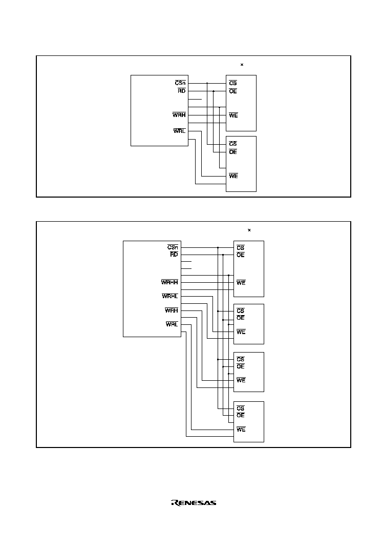
Rev. 2.0, 09/02, page 147 of 732
128k 8-bit
SRAM
This LSI
A0
A1 to 17
D8 to 15
D0 to 7
A0 to16
I/O0 to 7
A0 to 16
I/O0 to 7
Figure 9.14 Example of 16-bit Data Bus Width SRAM Connection
128k 8-bit
SRAM
This LSI
A0
A1
A2 to 18
D24 to 31
D16 to 23
D8 to 15
D0 to 7
A0 to 16
I/O0 to 7
A0 to 16
I/O0 to 7
A0 to 16
I/O0 to 7
A0 to 16
I/O0 to 7
Figure 9.15 Example of 32-bit Data Bus Width SRAM Connection (only for SH7145)
Rev. 2.0, 09/02, page 148 of 732
9.10
Access to On-chip Peripheral I/O Registers
On-chip peripheral I/O registers are accessed from the bus state controller as shown in table 9.3.
Refer to section 25, List of Registers, for more details.
Table 9.3 Access to On-chip Peripheral I/O Registers
On-chip
peripheral
module
SCI
MTU,
POE
INTC
PFC,
PORT
CMT
A/D
UBC
WDT
DMAC
DTC
IIC
H-UDI
Connection
bus width
8
bits
16
bits
16
bits
16
bits
16
bits
8
bits
16
bits
16
bits
16
bits
16
bits
8
bits
16
bits
Number of
access
cycles
2
cyc
2
cyc
2
cyc
2
cyc
2
cyc
3
cyc
3
cyc
3
cyc
3
cyc
3
cyc
2
cyc
2
cyc
9.11
Cycles of No-Bus Mastership Release
The bus mastership is not released during one bus cycle. For example, when the longword read (or
write) access is performed to the 8-bit normal space, four memory accesses to the 8-bit normal
space are regarded as one bus cycle. In this bus cycle, the bus mastership is not released. In this
case, assuming that one memory access takes two states, the bus mastership is not released in eight
states.
8 bits
8 bits
8 bits
8 bits
Cycle in which the bus
mastership is not released
Figure 9.16 One Bus Cycle
9.12
CPU Operation When Program Is Located in External Memory
In this LSI, two words (two instructions) are fetched in one instruction fetch. This also applies to
the cases where program is located in external memory or the bus width of that external memory is
8 or 16 bits.
Also, if the program counter value is the odd word (2n+1) address or the program counter value
before branch is the even word (2n) address, 32 bits (two instructions) including each word
instruction are always fetched.

DMASH20A_010020020700
Rev. 2.0, 09/02, page 149 of 732
Section 10 Direct Memory Access Controller (DMAC)
This LSI includes an on-chip four-channel direct memory access controller (DMAC). The DMAC
can be used in place of the CPU to perform high-speed data transfers among external devices
equipped with DACK (transfer request acknowledge signal), external memories, memory-mapped
external devices, and on-chip peripheral modules (except for the DMAC, DTC, BSC, and UBC).
Using the DMAC reduces the burden on the CPU and increases operating efficiency of the LSI as
a whole.
10.1
Features
∑
Four channels
∑
Four Gbytes of address space in the architecture
∑
Byte, word, or longword selectable data transfer unit
∑
16,777,216 transfers, maximum
∑
Address mode
Dual address mode or single address mode can be selected.
Direct access or indirect access can be selected in dual address mode.
∑
Channel function: Transfer modes that can be set are different for each channel.
Channel 0: Single or dual address mode. External requests are accepted.
Channel 1: Single or dual address mode. External requests are accepted.
Channel 2: Dual address mode only. Source address reload function is available.
Channel 3: Dual address mode only. Direct address transfer mode and indirect address
transfer mode selectable.
∑
Transfer requests: There are three DMAC transfer activation requests, as indicated below.
External request: From two
DREQ pins. DREQ can be detected either by falling edge or by
low level.
Requests from on-chip peripheral modules: Transfer requests from on-chip modules such
as SCI (request made to SCI_0 and SCI_1) or A/D (request made to A/D 1).
Auto-request: The transfer request is generated automatically within the DMAC.
∑
Selectable bus modes: Cycle-steal mode or burst mode
∑
Two types of DMAC channel priority ranking: Fixed priority mode or round robin mode
∑
CPU can be interrupted when the specified number of data transfers are complete.
∑
Module standby mode can be set.
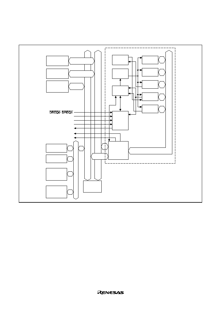
Rev. 2.0, 09/02, page 150 of 732
Figure 10.1 is a block diagram of the DMAC.
On-chip ROM
Peripheral bus
Internal bus
On-chip RAM
,
Transfer
count
control
SARn
DMAC module
Register
control
Activation
control
Request
priority
control
Bus interface
Bus state
controller
On-chip
peripheral
module
DARn
DMATCRn
CHCRn
DMAOR
MTU
SCI0, SCI1
A/D 1
DEIn
External
ROM
External
RAM
External I/O
(memory
mapped)
External I/O
(with
acknowledge)
DACK0, DACK1
DRAK0, DRAK1
SARn:
DARn:
DMATCRn:
CHCRn:
DMAOR:
n:
DMAC source address register
DMAC destination address register
DMAC transfer count register
DMAC channel control register
DMAC operation register
0, 1, 2, 3
Figure 10.1 DMAC Block Diagram

Rev. 2.0, 09/02, page 151 of 732
10.2
Input/Output Pins
Table 10.1 shows the DMAC pins.
Table 10.1 DMAC Pin Configuration
Channel
Name
Symbol
I/O
Function
0
DMA transfer request
DREQ0
I
DMA transfer request input from
external device to channel 0
DMA transfer request
acknowledge
DACK0
O
DMA transfer strobe output from
channel 0 to external device
DREQ0
acceptance
confirmation
DRAK0
O
Sampling receive acknowledge output
for DMA transfer request input from
external source
1
DMA transfer request
DREQ1
I
DMA transfer request input from
external device to channel 1
DMA transfer request
acknowledge
DACK1
O
DMA transfer strobe output from
channel 1 to external device
DREQ1
acceptance
confirmation
DRAK1
O
Sampling receive acknowledge output
for DMA transfer request input from
external source
10.3
Register Descriptions
DMAC has a total of 17 registers. Each channel has four control registers. One other control
register is shared by all channels. For register address and their states in each operating mode,
refer to section25, List of Registers.
∑
DMA source address register_0 (SAR_0)
∑
DMA destination address register_0 (DAR_0)
∑
DMA transfer count register_0 (DMATCR_0)
∑
DMA channel control register_0 (CHCR_0)
∑
DMA source address register_1 (SAR_1)
∑
DMA destination address register_1 (DAR_1)
∑
DMA transfer count register_1 (DMATCR_1)
∑
DMA channel control register_1 (CHCR_1)
∑
DMA source address register_2 (SAR_2)
∑
DMA destination address register_2 (DAR_2)
∑
DMA transfer count register_2 (DMATCR_2)
∑
DMA channel control register_2 (CHCR_2)
∑
DMA source address register_3 (SAR_3)

Rev. 2.0, 09/02, page 152 of 732
∑
DMA destination address register_3 (DAR_3)
∑
DMA transfer count register_3 (DMATCR_3)
∑
DMA channel control register_3 (CHCR_3)
∑
DMA operation register (DMAOR)
10.3.1
DMA Source Address Registers_0 to 3 (SAR_0 to SAR_3)
DMA source address registers_0 to 3 (SAR_0 to SAR_3) are 32-bit readable/writable registers
that specify the source address of a DMA transfer. These registers have a count function, and
during a DMA transfer, they indicate the next source address. In single-address mode, SAR values
are ignored when a device with DACK has been specified as the transfer source.
Specify a 16-bit or 32-bit boundary address when doing 16-bit or 32-bit data transfers. Operation
cannot be guaranteed on any other addresses.
When this register is accessed in 16 bits, the value of another 16 bits that are not accessed is
retained.
The initial value of SAR is undefined.
10.3.2
DMA Destination Address Registers_0 to 3 (DAR_0 to DAR_3)
DMA destination address registers_0 to 3 (DAR_0 to DAR_3) are 32-bit readable/writable
registers that specify the destination address of a DMA transfer. These registers have a count
function, and during a DMA transfer, they indicate the next destination address. In single-address
mode, DAR values are ignored when a device with DACK has been specified as the transfer
destination.
Specify a 16-bit or 32-bit boundary address when doing 16-bit or 32-bit data transfers. Operation
cannot be guaranteed on any other address. When this register is accessed in 16 bits, the value of
another 16 bits that are not accessed is retained.
The initial value of DAR is undefined.

Rev. 2.0, 09/02, page 153 of 732
10.3.3
DMA Transfer Count Registers_0 to 3 (DMATCR_0 to DMATCR_3)
DMA transfer count registers_0 to 3 (DMATCR_0 to DMATCR_3) are 32-bit readable/writable
registers that specify the transfer count for each channel (byte count, word count, or longword
count) with lower 24 bits. Specifying a H'000001 gives a transfer count of 1, while H'000000
gives the maximum setting, 16,777,216 transfers. While DMAC is in operation, the number of
transfers to be performed is indicated. Upper eight bits of this register are read as 0s and should
always be written with 0s.When this register is accessed in 16 bits, the value of another 16 bits
that are not accessed is retained.
The initial value of DMATCR is undefined.
10.3.4
DMA Channel Control Registers_0 to 3 (CHCR_0 to CHCR_3)
DMA channel control registers_0 to 3 (CHCR_0 to CHCR_3) is a 32-bit readable/writable register
where the operation and transmission of each channel is designated.
Bit
Bit Name
Initial Value
R/W
Description
31
30
29
28
27
26
25
24
23
22
21
0
0
0
0
0
0
0
0
0
0
0
R
R
R
R
R
R
R
R
R
R
R
Reserved
These bits are read as 0s and should always be
written with 0s.
20
DI
0
(R/W)
*
2
Direct/Indirect
Specifies either direct address mode operation or
indirect address mode operation for channel 3
source address. This bit is valid only in CHCR_3.
For CHCR0 to CHCR2, this bit is always read as 0
and should always be written with 0.
0: Direct access mode operation for channel 3
1: Indirect access mode operation for channel 3
19
RO
0
(R/W)
*
2
Source Address Reload
Selects whether to reload the source address initial
value during channel 2 transfer. This bit is valid only
for channel 2. For CHCR_0, 1 ,3, this bit is always
read as 0 and should always be written with 0.
0: Does not reload source address
1: Reloads source address

Rev. 2.0, 09/02, page 154 of 732
Bit
Bit Name
Initial Value
R/W
Description
18
RL
0
(R/W)
*
2
Request Check Level
Selects whether to output DRAK notifying external
device of
DREQ
received, with active high or active
low. This bit is valid only for CHCR_0 and CHCR_1.
For CHCR_2 and CHCR_3, this bit is always read
as 0 and should always be written with 0.
0: Output DRAK with active high
1: Output DRAK with active low
17
AM
0
(R/W)
*
2
Acknowledge Mode
In dual address mode, selects whether to output
DACK in the data write cycle or data read cycle. In
single address mode, DACK is always output
irrespective of the setting of this bit. This bit is valid
only for CHCR_0 and CHCR_1. For CHCR_2 and
CHCR_3, this bit is always read as 0 and should
always be written with 0.
0: Outputs DACK during read cycle
1: Outputs DACK during write cycle
16
AL
0
(R/W)
*
2
Acknowledge Level
Specifies whether to set DACK (acknowledge)
signal output to active high or active low. This bit is
valid only with CHCR_0 and CHCR_1. For
CHCR_2 and CHCR_3, this bit is always read as 0
and should always be written with 0.
0: Active high output
1: Active low output
15
14
DM1
DM0
0
0
R/W
R/W
Destination Address Mode 1, 0
These bits specify increment/decrement of the DMA
transfer destination address. These bit
specifications are ignored when transferring data
from an external device to address space in single
address mode.
00: Destination address fixed
01: Destination address incremented (+1 during 8-
bit transfer, +2 during 16-bit transfer, +4 during
32-bit transfer)
10: Destination address decremented (≠1 during 8-
bit transfer, ≠2 during 16-bit transfer, ≠4 during
32-bit transfer)
11: Setting prohibited

Rev. 2.0, 09/02, page 155 of 732
Bit
Bit Name
Initial Value
R/W
Description
13
12
SM1
SM0
0
0
R/W
R/W
Source Address Mode 1, 0
These bits specify increment/decrement of the DMA
transfer source address. These bit specifications
are ignored when transferring data from an external
device to address space in single address mode.
00: Source address fixed
01: Source address incremented (+1 during 8-bit
transfer, +2 during 16-bit transfer, +4 during 32-
bit transfer)
10: Source address decremented (≠1 during 8-bit
transfer, ≠2 during 16-bit transfer, ≠4 during 32-
bit transfer)
11: Setting prohibited
When the transfer source is specified at an indirect
address, specify in source address register 3
(SAR_3) the actual storage address of the data you
want to transfer as the data storage address
(indirect address).
During indirect address mode, SAR_3 obeys the
SM1/SM0 setting for increment/decrement. In this
case, SAR_3's increment/decrement is fixed at +4/≠
4 or 0, irrespective of the transfer data size
specified by TS1 and TS0.

Rev. 2.0, 09/02, page 156 of 732
Bit
Bit Name
Initial Value
R/W
Description
11
10
9
8
RS3
RS2
RS1
RS0
0
0
0
0
R/W
R/W
R/W
R/W
Resource Select 3, 2, 1, 0
These bits specify the transfer request source.
0000: External request, dual address mode
0001: Prohibited
0010: External request, single address mode.
External address space
external device.
0011: External request, single address mode.
External device
external address space.
0100: Auto-request
0101: Prohibited
0110: MTU TGIA_0
0111: MTU TGIA_1
1000: MTU TGIA_2
1001: MTU TGIA_3
1010: MTU TGIA_4
1011: A/D1 ADI1
1100: SCI0 TXI_0
1101: SCI0 RXI_0
1110: SCI1 TXI_1
1111: SCI1 RXI_1
Note:
External request designations are valid only
for channels 0 and 1. No transfer request
sources can be set for channels 2 or 3.
7
0
R
Reserved
This bit is always read as 0 and should always be
written with 0

Rev. 2.0, 09/02, page 157 of 732
Bit
Bit Name
Initial Value
R/W
Description
6
DS
0
(R/W)
*
2
DREQ
Select
Sets the sampling method for the
DREQ
pin in
external request mode to either low-level detection
or falling-edge detection. This bit is valid only with
CHCR_0 and CHCR_1. For CHCR_2 and
CHCR_3, this bit is always read as 0 and should
always be written with 0.
Even with channels 0 and 1, when specifying an on-
chip peripheral module or auto-request as the
transfer request source, this bit setting is ignored.
The sampling method is fixed at falling-edge
detection in cases other than auto-request.
0: Low-level detection
1: Falling-edge detection
5
TM
0
R/W
Transfer Mode
Specifies the bus mode for data transfer.
0: Cycle steal mode
1: Burst mode
4
3
TS1
TS0
0
0
R/W
R/W
Transfer Size 1, 0
Specify size of data for transfer.
00: Specifies byte size (8 bits)
01: Specifies word size (16 bits)
10: Specifies longword size (32 bits)
11: Prohibited
2
IE
0
R/W
Interrupt Enable
When this bit is set to 1, interrupt requests are
generated after the number of data transfers
specified in the DMATCR (when TE = 1).
0: Interrupt request not generated after DMATCR-
specified transfer count
1: Interrupt request enabled on completion of
DMATCR specified number of transfers

Rev. 2.0, 09/02, page 158 of 732
Bit
Bit Name
Initial Value
R/W
Description
1
TE
0
R/(W)
*
1
Transfer End Flag
This bit is set to 1 after the number of data transfers
specified by the DMATCR. At this time, if the IE bit
is set to 1, an interrupt request is generated.
If data transfer ends before TE is set to 1 (for
example, due to an NMI or address error, or
clearing of the DE bit or DME bit of the DMAOR)
the TE is not set to 1. With this bit set to 1, data
transfer is disabled even if the DE bit is set to 1.
0: DMATCR-specified transfer count not ended
Clear condition:
0 write after TE = 1 read, Power-on reset, software
standby mode
1: DMATCR specified number of transfers
completed
0
DE
0
R/W
DMAC Enable
DE enables operation in the corresponding channel.
0: Operation of the corresponding channel disabled
1: Operation of the corresponding channel enabled
Transfer mode is entered if this bit is set to 1 when
auto-request is specified (RS3 to RS0 settings).
With an external request or on-chip module request,
when a transfer request occurs after this bit is set to
1, transfer is enabled. If this bit is cleared during a
data transfer, transfer is suspended.
If the DE bit has been set, but TE = 1, then if the
DME bit of the DMAOR is 0, and the NMI or AE bit
of the DMAOR is 1, transfer enable mode is not
entered.
Notes: 1. TE bit: Allows only 0 write after reading 1.
2. The DI, RO, RL, AM, AL, or DS bit may be absent, depending on the channel.

Rev. 2.0, 09/02, page 159 of 732
10.3.5
DMAC Operation Register (DMAOR)
The DMAOR is a 16-bit readable/writable register that specifies the transfer mode of the DMAC
Bit
Bit Name
Initial Value
R/W
Description
15 to
10
All 0
R
Reserved
These bits are always read as 0s and should
always be written with 0s.
9
8
PR1
PR0
0
0
R/W
R/W
Priority Mode 1 and 0
These bits determine the priority level of channels
for execution when transfer requests are made for
several channels simultaneously.
00: CH0
>
CH1
>
CH2
>
CH3
01: CH0
>
CH2
>
CH3
>
CH1
10: CH2
>
CH0
>
CH1
>
CH3
11: Round robin mode
7 to 3
All 0
R
Reserved
These bits are read as 0s and should always be
written with 0s.
2
AE
0
R/(W)
*
Address Error Flag
Indicates that an address error has occurred during
DMA transfer. If this bit is set during a data
transfer, transfers on all channels are suspended.
The CPU cannot write a 1 to the AE bit. Clearing is
effected by 0 write after 1 read.
0: No address error, DMA transfer enabled
Clearing condition:
Write AE = 0 after reading AE = 1
1: Address error, DMA transfer disabled
Setting condition:
Address error due to DMAC

Rev. 2.0, 09/02, page 160 of 732
Bit
Bit Name
Initial Value
R/W
Description
1
NMIF
0
R/(W)
*
NMI Flag
Indicates input of an NMI. This bit is set
irrespective of whether the DMAC is operating or
suspended. If this bit is set during a data transfer,
transfers on all channels are suspended. The CPU
is unable to write a 1 to the NMIF. Clearing is
effected by a 0 write after 1 read.
0: No NMI interrupt, DMA transfer enabled
Clearing condition:
Write NMIF = 0 after reading NMIF = 1
1: NMI has occurred, DMA transfer prohibited
Set condition:
NMI interrupt occurrence
0
DME
0
R/W
DMAC Master Enable
This bit enables activation of the entire DMAC.
When the DME bit and DE bit of the CHCR for the
corresponding channel are set to 1, that channel is
transfer-enabled. If this bit is cleared during a data
transfer, transfers on all channels are suspended.
0: Disable operation on all channels
1: Enable operation on all channels
Even when the DME bit is set, when the TE bit of
the CHCR is 1, or its DE bit is 0, transfer is
disabled when NMI of the DMAOR = 1 or when AE
= 1.
Note:
*
Only 0 can be written to clear the flag.

Rev. 2.0, 09/02, page 161 of 732
10.4
Operation
When there is a DMA transfer request, the DMAC starts the transfer according to the
predetermined channel priority order; when the transfer end conditions are satisfied, it ends the
transfer. Transfers can be requested in three modes: auto-request, external request, and on-chip
peripheral module request. Transfer can be in either the single address mode or the dual address
mode, and dual address mode can be either direct or indirect address transfer mode. The bus mode
can be either burst or cycle steal.
10.4.1
DMA Transfer Flow
After the DMA source address registers (SAR), DMA destination address registers (DAR), DMA
transfer count register (DMATCR), DMA channel control registers (CHCR), and DMA operation
register (DMAOR) are set to the desired transfer conditions, the DMAC transfers data according
to the following procedure:
1. The DMAC checks to see if transfer is enabled (DE = 1, DME = 1, TE = 0, NMIF = 0,
AE = 0).
2. When a transfer request comes and transfer has been enabled, the DMAC transfers 1 transfer
unit of data (determined by TS0 and TS1 setting). For an auto-request, the transfer begins
automatically when the DE bit and DME bit are set to 1. The DMATCR value will be
decremented by 1 upon each transfer. The actual transfer flows vary by address mode and bus
mode.
3. When the specified number of transfers have been completed (when DMATCR reaches 0), the
transfer ends normally. If the IE bit of the CHCR is set to 1 at this time, a DEI interrupt is sent
to the CPU.
4. When an address error occurs in the DMAC or an NMI interrupt is generated, the transfer is
aborted. Transfers are also aborted when the DE bit of the CHCR or the DME bit of the
DMAOR are changed to 0.
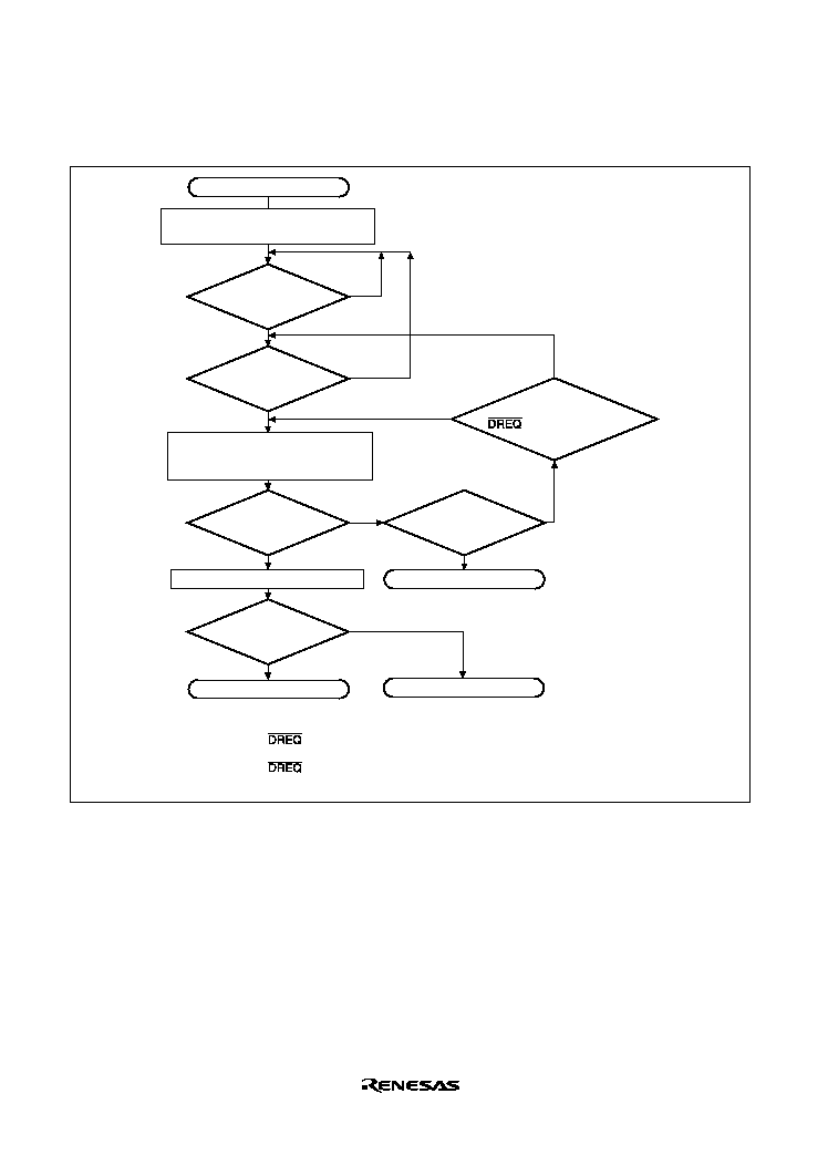
Rev. 2.0, 09/02, page 162 of 732
Figure 10.2 is a flowchart of this procedure.
Normal end
Does
NMIF = 1, AE = 1,
DE = 0, or DME
= 0?
Bus mode,
transfer request mode,
detection selection
system
Initial settings
(SAR, DAR, DMATCR, CHCR, DMAOR)
Transfer (1 transfer unit);
DMATCR ≠ 1
DMATCR,
SAR and DAR updated
DEI interrupt request (when IE = 1)
No
Yes
No
Yes
No
Yes
Yes
No
Yes
No
*
3
*
2
Start
Transfer aborted
Notes:
1.
2.
3.
In auto-request mode, transfer begins when NMIF, AE, and TE are all 0,
and the DE and DME bits are set to 1.
= level detection in burst mode (external request) or cycle-steal
mode.
= edge detection in burst mode (external request), or auto-request
mode in burst mode.
DMATCR = 0?
Transfer request
occurs?
*
1
DE, DME = 1 and
NMIF, AE, TE = 0?
Does
NMIF = 1, AE = 1,
DE = 0, or DME
= 0?
Transfer ends
Figure 10.2 DMAC Transfer Flowchart

Rev. 2.0, 09/02, page 163 of 732
10.4.2
DMA Transfer Requests
DMA transfer requests are usually generated in either the data transfer source or destination, but
they can also be generated by devices and on-chip peripheral modules that are neither the source
nor the destination. Transfers can be requested in three modes: auto-request, external request, and
on-chip peripheral module request. The request mode is selected in the RS3 to RS0 bits of the
DMA channel control registers 0 to 3 (CHCR0 to CHCR3).
Auto-Request Mode: When there is no transfer request signal from an external source, as in a
memory-to-memory transfer or a transfer between memory and an on-chip peripheral module
unable to request a transfer, the auto-request mode allows the DMAC to automatically generate a
transfer request signal internally. When the DE bits of CHCR0 to CHCR3 and the DME bit of the
DMAOR are set to 1, the transfer begins (so long as the TE bits of CHCR0 to CHCR3 and the
NMIF and AE bits of DMAOR are all 0).
External Request Mode: In this mode a transfer is performed at the request signal (
DREQ) of an
external device. Choose one of the modes shown in table 10.2 according to the application system.
When this mode is selected, if the DMA transfer is enabled (DE = 1, DME = 1, TE = 0, NMIF = 0,
AE = 0), a transfer is performed upon a request at the
DREQ input. Choose to detect DREQ by
either the falling edge or low level of the signal input with the DS bit of CHCR0 to CHCR3 (DS =
0 is level detection, DS = 1 is edge detection). The source of the transfer request does not have to
be the data transfer source or destination.
Table 10.2 Selecting External Request Modes with the RS Bits
RS3
RS2
RS1
RS0
Address Mode
Source
Destination
0
0
0
0
Dual address
mode
Any
*
Any
*
0
0
1
0
Single address
mode
External memory or
memory-mapped
external device
External device with
DACK
0
0
1
1
Single address
mode
External device with
DACK
External memory or
memory-mapped
external device
Note:
*
External memory, memory-mapped external device, on-chip memory, on-chip peripheral
module (excluding DMAC, DTC, BSC, UBC).
On-Chip Peripheral Module Request Mode: In this mode a transfer is performed at the transfer
request signal (interrupt request signal) of an on-chip peripheral module. As indicated in table
10.3, there are ten transfer request signals: five from the multifunction timer pulse unit (MTU),
which are compare match or input capture interrupts; the receive data full interrupts (RXI) and
transmit data empty interrupts (TXI) of the two serial communication interfaces (SCI); and the
A/D conversion end interrupt (ADI1) of the A/D converter. When DMA transfers are enabled (DE

Rev. 2.0, 09/02, page 164 of 732
= 1, DME = 1, TE = 0, NMIF = 0, AE = 0), a transfer is performed upon the input of a transfer
request signal.
The transfer request source need not be the data transfer source or transfer destination. However,
when the transfer request is set by RXI (transfer request because SCI's receive data is full), the
transfer source must be the SCI's receive data register (RDR). When the transfer request is set by
TXI (transfer request because SCI's transmit data is empty), the transfer destination must be the
SCI's transmit data register (TDR). Also, if the transfer request is set to the A/D converter, the
data transfer destination must be the A/D converter register.
Table 10.3 Selecting On-Chip Peripheral Module Request Modes with the RS Bits
RS3 RS2 RS1 RS0
DMAC Transfer
Request Source
DMA Transfer
Request Signal Source
Desti-
nation
Bus Mode
0
1
1
0
MTU
TGIA_0
Any
*
Any
*
Burst/cycle steal
0
1
1
1
MTU
TGIA_1
Any
*
Any
*
Burst/cycle steal
1
0
0
0
MTU
TGIA_2
Any
*
Any
*
Burst/cycle steal
1
0
0
1
MTU
TGIA_3
Any
*
Any
*
Burst/cycle steal
1
0
1
0
MTU
TGIA_4
Any
*
Any
*
Burst/cycle steal
1
0
1
1
A/D1
ADI1
ADDR1
Any
*
Burst/cycle steal
1
1
0
0
SCI0 transmit block
TXI_0
Any
*
TDR0
Burst/cycle steal
1
1
0
1
SCI0 receiver block
RXI_0
RDR0
Any
*
Burst/cycle steal
1
1
1
0
SCI1 transmit block
TXI_1
Any
*
TDR1
Burst/cycle steal
1
1
1
1
SCI1 receiver block
RXI_1
RDR1
Any
*
Burst/cycle steal
Notes:
*
External memory, memory-mapped external device, on-chip memory, on-chip peripheral
module (excluding DMAC, DTC, BSC, UBC).
MTU: Multifunction timer pulse unit.
SCI0, SCI1: Serial communications interface channels 0 and 1.
ADDR1: A/D converter's A/D register.
TDR_0, TDR_1: SCI_0 and SCI_1 transmit data registers.
RDR_0, RDR_1: SCI_0 and SCI_1 receive data registers.
In order to output a transfer request from an on-chip peripheral module, set the relevant interrupt
enable bit for each module, and output an interrupt signal.
When an on-chip peripheral module's interrupt request signal is used as a DMA transfer request
signal, interrupts for the CPU are not generated.
When a DMA transfer is conducted corresponding with one of the transfer request signals in table
10.3, it is automatically discontinued. In cycle steal mode this occurs in the first transfer, and in
burst mode in the last transfer.

Rev. 2.0, 09/02, page 165 of 732
10.4.3
Channel Priority
When the DMAC receives simultaneous transfer requests on two or more channels, it selects a
channel according to a predetermined priority order, either in a fixed mode or in round robin
mode. These modes are selected by priority bits PR1 and PR0 in the DMA operation register
(DMAOR).
Fixed Mode: In this mode, the priority levels among the channels remain fixed.
The following priority orders are available for fixed mode:
∑
CH0
>
CH1
>
CH2
>
CH3
∑
CH0
>
CH2
>
CH3
>
CH1
∑
CH2
>
CH0
>
CH1
>
CH3
These are selected by settings of the PR1 and PR0 bits of the DMA operation register (DMAOR).
Round Robin Mode: In round robin mode, each time the transfer of one transfer unit (byte, word
or long word) ends on a given channel, that channel receives the lowest priority level (figure 10.3
(1) ). The priority level in round robin mode immediately after a reset is CH0
>
CH1
>
CH2
>
CH3.
Rev. 2.0, 09/02, page 166 of 732
CH1
>
CH2
>
CH3
>
CH0
CH0
>
CH1
>
CH2
>
CH3
CH2
>
CH3
>
CH0
>
CH1
CH0
>
CH1
>
CH2
>
CH3
CH2
>
CH3
>
CH0
>
CH1
CH0
>
CH1
>
CH2
>
CH3
CH0
>
CH1
>
CH2
>
CH3
CH3
>
CH0
>
CH1
>
CH2
CH0
>
CH1
>
CH2
>
CH3
Transfer on channel 0
Initial priority setting
Initial priority setting
Initial priority setting
Initial priority setting
No change in priority.
When channel 2 receives the
lowest priority, the priorities
of channel 0 and 1, which
were above channel 2, are also
shifted simultaneously. Immedi-
ately thereafter, if there is a transfer
request for channel 1 only, channel
1 is given the lowest priority,
and the priorities of channels 3
and 0 are simultaneously
shifted down.
When channel 1 is given the
lowest priority, the priority
of channel 0, which was
above channel 1, is also shifted
simultaneously.
Channel 0 is given the lowest
priority.
Priority after transfer
Priority after transfer
Priority after transfer
Priority after transfer
Priority after transfer
due to issue of a transfer
request for channel 1
only.
Transfer on channel 1
Transfer on channel 2
Transfer on channel 3
Figure 10.3 (1) Round Robin Mode
Rev. 2.0, 09/02, page 167 of 732
Figure 10.3 (2) shows the changes in priority levels when transfer requests are issued
simultaneously for channels 0 and 3, and channel 1 receives a transfer request during a transfer on
channel 0. The DMAC operates in the following manner under these circumstances:
1. Transfer requests are issued simultaneously for channels 0 and 3.
2. Since channel 0 has a higher priority level than channel 3, the channel 0 transfer is conducted
first (channel 3 is on transfer standby).
3. A transfer request is issued for channel 1 during a transfer on channel 0 (channels 1 and 3 are
on transfer standby).
4. At the end of the channel 0 transfer, channel 0 shifts to the lowest priority level.
5. At this point, channel 1 has a higher priority level than channel 3, so the channel 1 transfer
comes first (channel 3 is on transfer standby).
6. When the channel 1 transfer ends, channel 1 shifts to the lowest priority level.
7. Channel 3 transfer begins.
8. When the channel 3 transfer ends, channel 3 and channel 2 priority levels are lowered, giving
channel 3 the lowest priority.
Transfer request
Channel waiting
DMAC operation
Channel priority
Issued for
channels 0 and 3
Issued for channel 1
0
>
1
>
2
>
3
Channel 0
transfer begins
1
>
2
>
3
>
0
Channel 0
transfer ends
Channel 1
transfer begins
Channel 3
transfer begins
2
>
3
>
0
>
1
Channel 1
transfer ends
0
>
1
>
2
>
3
Channel 3
transfer ends
Change of
priority
Change of
priority
Change of
priority
None
3
3
1,3
Figure 10.3 (2) Example of Changes in Priority in Round Robin Mode

Rev. 2.0, 09/02, page 168 of 732
10.4.4
DMA Transfer Types
The DMAC supports the transfers shown in table 10.4. It can operate in the single address mode,
in which either the transfer source or destination is accessed using an acknowledge signal, or dual
access mode, in which both the transfer source and destination addresses are output. The dual
access mode consists of a direct address mode, in which the output address value is the object of a
direct data transfer, and an indirect address mode, in which the output address value is not the
object of the data transfer, but the value stored at the output address becomes the transfer object
address. The actual transfer operation timing varies with the bus mode. The DMAC has two bus
modes: cycle-steal mode and burst mode.
Table 10.4 Supported DMA Transfers
Destination
Source
External Device
with DACK
External
Memory
Memory-
Mapped
External
Device
On-Chip
Memory
On-Chip
Peripheral
Module
External device with DACK Not available
Single
Single
Not available
Not available
External memory
Single
Dual
Dual
Dual
Dual
Memory-mapped external
device
Single
Dual
Dual
Dual
Dual
On-chip memory
Not available
Dual
Dual
Dual
Dual
On-chip peripheral module
Not available
Dual
Dual
Dual
Dual
Note:
Dual address mode includes both direct address mode and indirect address mode.
Address Modes
Single Address Mode: In the single address mode, both the transfer source and destination are
external; one is accessed by a DACK signal while the other is accessed by an address. In this
mode, the DMAC performs the DMA transfer in 1 bus cycle by simultaneously outputting a
transfer request acknowledge DACK signal to one external device to access it while outputting an
address to the other end of the transfer. Figure 10.4 shows an example of a transfer between an
external memory and an external device with DACK in which the external device outputs data to
the data bus while that data is written in external memory in the same bus cycle.
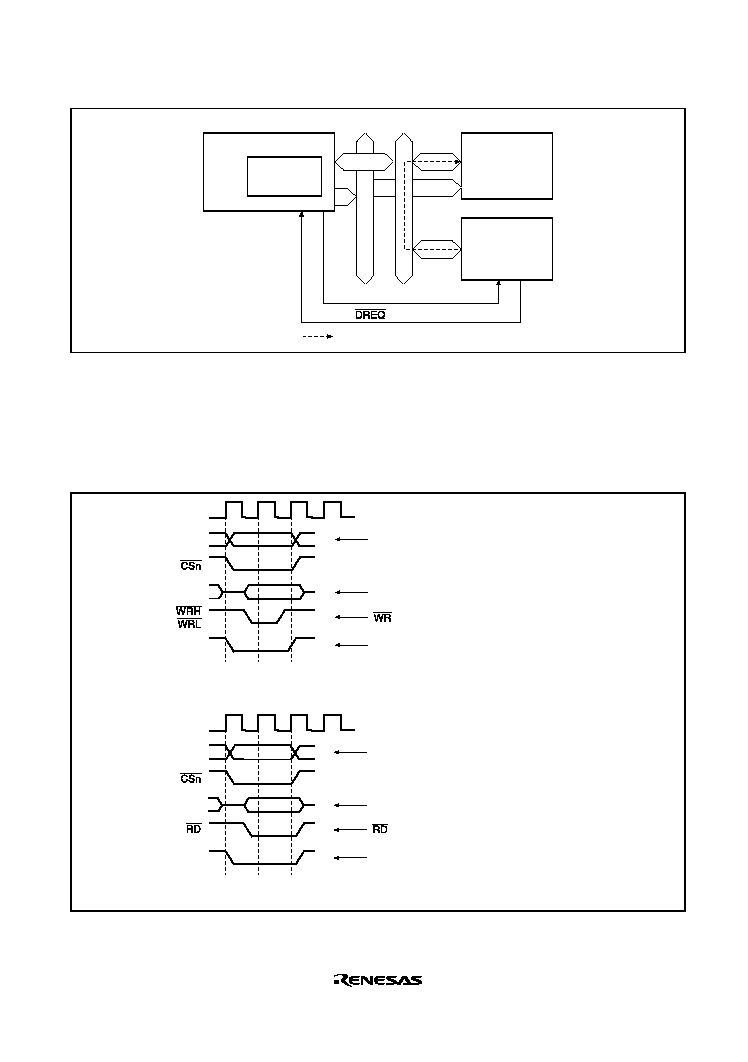
Rev. 2.0, 09/02, page 169 of 732
DMAC
DACK
External
memory
External device
with DACK
This LSI
External address bus
: Data flow
External data bus
Figure 10.4 Data Flow in Single Address Mode
Two types of transfers are possible in the single address mode: (a) transfers between external
devices with DACK and memory-mapped external devices, and (b) transfers between external
devices with DACK and external memory. The only transfer requests for either of these is the
external request (
DREQ). Figure 10.5 shows the DMA transfer timing for the single address mode.
CK
A21≠A0
D15≠D0
DACK
Address output to external memory space
Data that is output from the external
device with DACK
DACK signal to external devices with
DACK (active low)
signal to external memory space
a. External device with DACK to external memory space
CK
A21≠A0
D15≠D0
Address output to external memory space
Data that is output from external memory space
signal to external memory space
DACK signal to external device with DACK
(active low)
DACK
b. External memory space to external device with DACK
Figure 10.5 Example of DMA Transfer Timing in the Single Address Mode

Rev. 2.0, 09/02, page 170 of 732
Dual Address Mode
Dual address mode is used for access of both the transfer source and destination by address.
Transfer source and destination can be accessed either internally or externally. Dual address mode
is subdivided into two other modes: direct address transfer mode and indirect address transfer
mode.
Direct Address Transfer Mode: Data is read from the transfer source during the data read cycle,
and written to the transfer destination during the write cycle, so transfer is conducted in two bus
cycles. At this time, the transfer data is temporarily stored in the DMAC. With the kind of external
memory transfer shown in figure 10.6, data is read from one of the memories by the DMAC
during a read cycle, then written to the other external memory during the subsequent write cycle.
Figure 10.7 shows the timing for this operation.
Data buffer
Address b
u
s
Data b
u
s
Address b
u
s
Data b
u
s
Memory
Transfer source
module
Transfer destination
module
Memory
Transfer source
module
Transfer destination
module
SAR
DAR
Data buffer
SAR
DAR
The SAR value is taken as the address, and data is read from the transfer source
module and stored temporarily in the DMAC.
1st bus cycle
2nd bus cycle
The DAR value is taken as the address, and data stored in the DMAC's data
buffer is written to the transfer destination module.
DMAC
DMAC
Figure 10.6 Direct Address Operation during Dual Address Mode
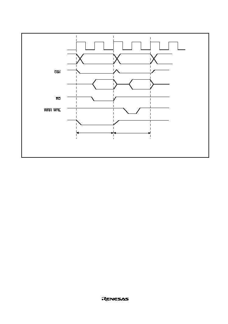
Rev. 2.0, 09/02, page 171 of 732
Data read cycle
Data write cycle
Transfer destination
address
Transfer source
address
CK
(1st cycle)
(2nd cycle)
A21≠A0
D15≠D0
,
DACK
Note:
Transfer between external memories with DACK are output during read cycle.
Figure 10.7 Example of Direct Address Transfer Timing in Dual Address Mode
Indirect Address Transfer Mode: In this mode the memory address storing the data you actually
want to transfer is specified in DMAC internal transfer source address register (SAR3). Therefore,
in indirect address transfer mode, the DMAC internal transfer source address register value is read
first. This value is stored once in the DMAC. Next, the read value is output as the address, and the
value stored at that address is again stored in the DMAC. Finally, the subsequent read value is
written to the address specified by the transfer destination address register, ending one cycle of
DMA transfer.
In indirect address mode (figure 10.8), transfer destination, transfer source, and indirect address
storage destination are all 16-bit external memory locations, and transfer in this example is
conducted in 16-bit or 8-bit units. Timing for this transfer example is shown in figure 10.9.
In indirect address mode, one NOP cycle (figure 10.9) is required until the data read as the indirect
address is output to the address bus. When transfer data is 32-bit, the third and fourth bus cycles
each need to be doubled, giving a required total of six bus cycles and one NOP cycle for the whole
operation.
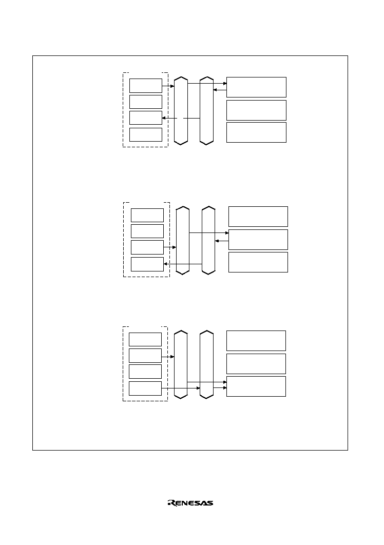
Rev. 2.0, 09/02, page 172 of 732
SAR3
DAR3
Data
buffer
Address b
u
s
Data b
u
s
Memory
Transfer source
module
Transfer destination
module
Temporary
buffer
The SAR3 value is taken as the address, memory data is read, and the value is stored in the
temporary buffer. Since the value read at this time is used as the address, it must be 32 bits.
When external connection data bus is 16 bits, two bus cycles are required.
DMAC
SAR3
DAR3
Data
buffer
Address b
u
s
Data b
u
s
Memory
Transfer source
module
Transfer destination
module
Temporary
buffer
The value in the temporary buffer is taken as the address, and data is read from the
transfer source module to the data buffer.
SAR3
DAR3
Data
buffer
Address b
u
s
Data b
u
s
Memory
Transfer source
module
Transfer destination
module
Temporary
buffer
The DAR3 value is taken as the address, and the value in the data buffer is written to the
transfer destination module.
Note:
Memory, transfer source, and transfer destination modules are shown here. In
practice, connection can be made anywhere if there is address space.
DMAC
DMAC
1st, 2nd bus cycles
3rd bus cycle
4th bus cycle
Figure 10.8 Dual Address Mode and Indirect Address Operation
(When External Memory Space is 16 bits)
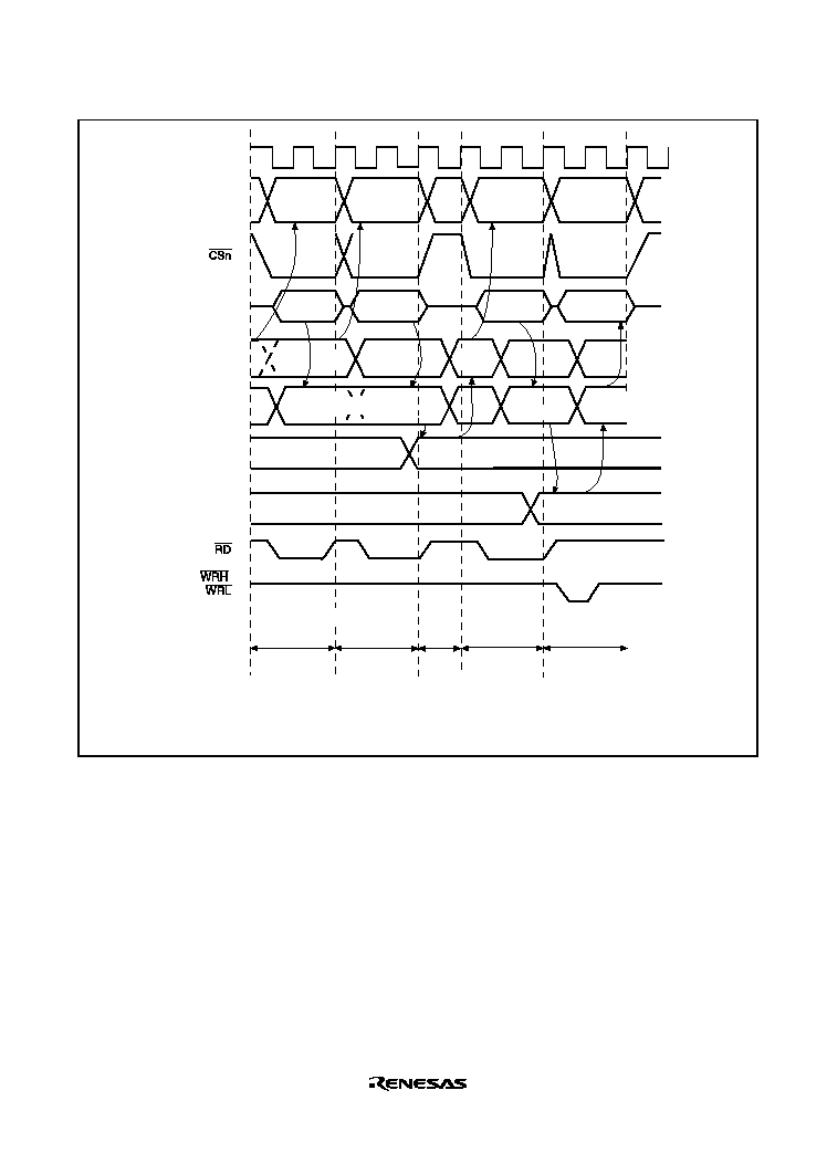
Rev. 2.0, 09/02, page 173 of 732
Transfer
source
address (H)
Transfer
source
address (L)
Indirect
address
NOP
Transfer
destination
address
Indirect
address (H)
Indirect
address (L)
Transfer
data
Transfer
data
Transfer
data
Transfer
data
Transfer
data
Transfer source
address
1
Indirect address
2
Indirect
address
NOP
Indirect
address
Address read cycle
(1st)
(2nd)
(3rd)
NOP
cycle
Data
read cycle
(4th)
Data
write cycle
CK
A21≠A0
D15≠D0
Internal
address
bus
Internal
data bus
DMAC
indirect
address
buffer
DMAC
data
buffer
,
Notes:
1.
2.
The internal address bus is controlled by the port and does not change.
DMAC does not fetch value until 32-bit data is read from the internal data
bus.
Figure 10.9 Dual Address Mode and Indirect Address Transfer Timing Example
(External Memory Space to External Memory Space, 16-bit width)
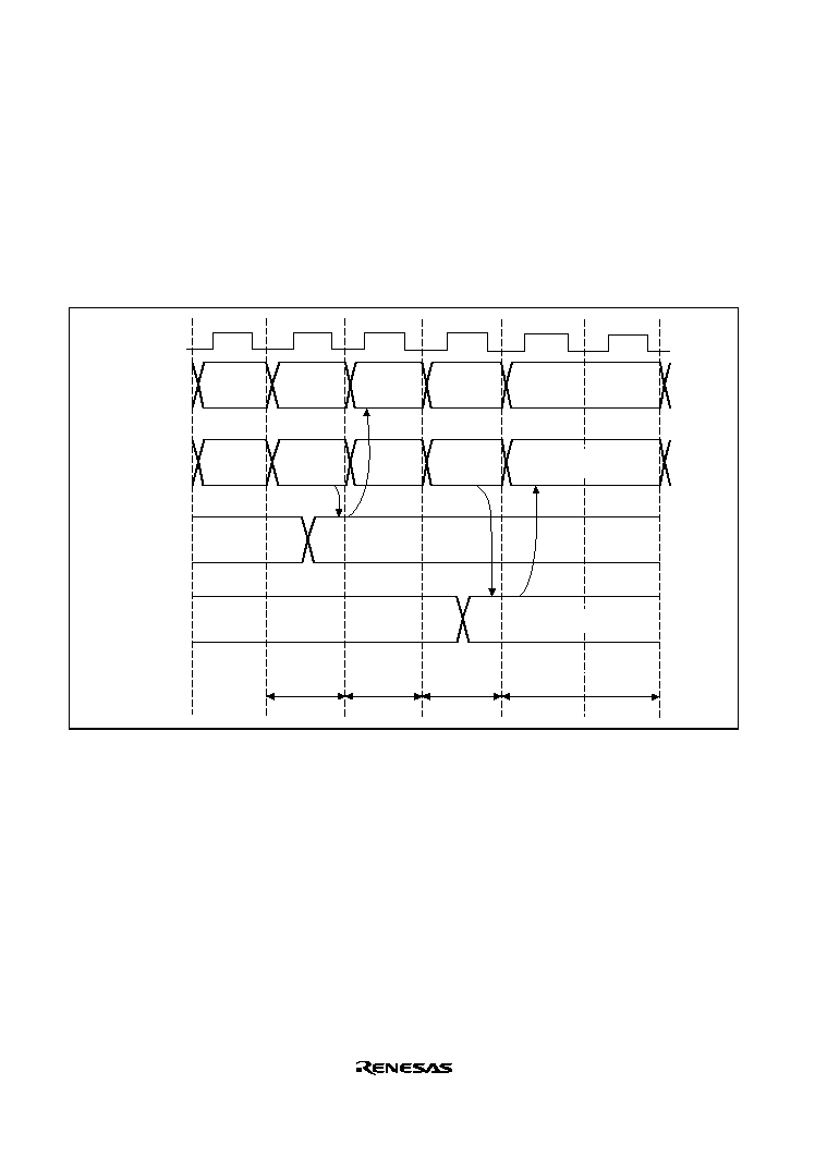
Rev. 2.0, 09/02, page 174 of 732
Figure 10.10 shows an example of timing in indirect address mode when transfer source and
indirect address storage locations are in internal memory, the transfer destination is an on-chip
peripheral module with 2-cycle access space, and transfer data is 8-bit.
Since the indirect address storage destination and the transfer source are in internal memory, these
can be accessed in one cycle. The transfer destination is 2-cycle access space, so two data write
cycles are required. One NOP cycle is required until the data read as the indirect address is output
to the address bus.
Internal
address
bus
Internal
data
bus
DMAC
indirect
address
buffer
DMAC
data
buffer
CK
Transfer
source
address
NOP
NOP
Indirect
address
Transfer
destination
address
Indirect
address
Indirect
address
Transfer
data
Transfer data
Transfer data
Address
read cycle
NOP
cycle
Data
read cycle
Data write cycle (4th)
(1st)
(2nd)
(3rd)
Figure 10.10 Dual Address Mode and Indirect Address Transfer Timing Example
(On-chip Memory Space to On-chip Memory Space)
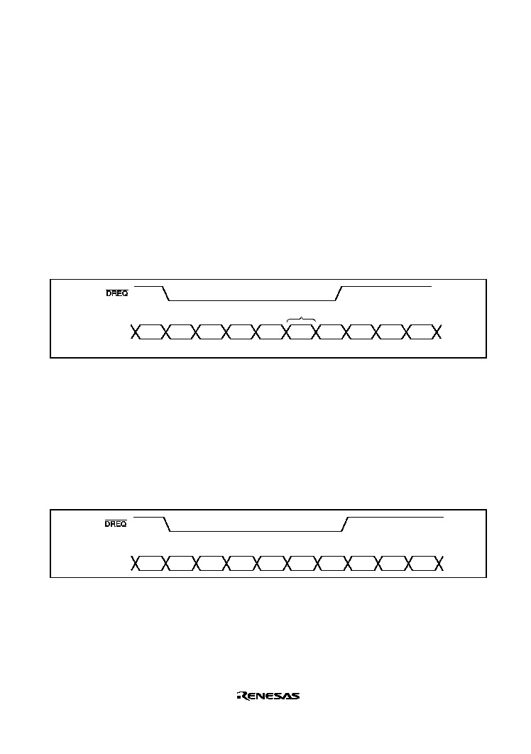
Rev. 2.0, 09/02, page 175 of 732
Bus Modes
Select the appropriate bus mode in the TM bits of CHCR0 to CHCR3. There are two bus modes:
cycle steal and burst.
Cycle-Steal Mode: In the cycle steal mode, the bus mastership is given to another bus master after
each one-transfer-unit (byte, word, or longword) DMAC transfer. When the next transfer request
occurs, the bus mastership are obtained from the other bus master and a transfer is performed for
one transfer unit. When that transfer ends, the bus mastership is passed to the other bus master.
This is repeated until the transfer end conditions are satisfied.
The cycle steal mode can be used with all categories of transfer destination, transfer source and
transfer request. Figure 10.11 shows an example of DMA transfer timing in the cycle steal mode.
Transfer conditions are dual address mode and
DREQ level detection.
CPU
CPU
CPU
DMAC
DMAC
CPU
DMAC
DMAC
CPU
CPU
Bus cycle
Bus control returned to CPU
Read
Write
Write
Read
Figure 10.11 DMA Transfer Example in the Cycle-Steal Mode
Burst Mode: Once the bus mastership is obtained, the transfer is performed continuously until the
transfer end condition is satisfied. In the external request mode with low level detection of the
DREQ pin, however, when the DREQ pin is driven high, the bus passes to the other bus master
after the bus cycle of the DMAC that currently has an acknowledged request ends, even if the
transfer end conditions have not been satisfied.
Figure 10.12 shows an example of DMA transfer timing in the burst mode. Transfer conditions are
single address mode and
DREQ level detection.
CPU
CPU
CPU
DMAC
DMAC
DMAC
DMAC
DMAC
Bus cycle
DMAC
CPU
Figure 10.12 DMA Transfer Example in the Burst Mode

Rev. 2.0, 09/02, page 176 of 732
Relationship between Request Modes and Bus Modes by DMA Transfer Category
Table 10.5 shows the relationship between request modes and bus modes by DMA transfer
category.
Table 10.5 Relationship of Request Modes and Bus Modes by DMA Transfer Category
Address
Mode
Transfer Category
Request
Mode
Bus
Mode
Transfer
Size (Bits)
Usable
Channels
Single
External device with DACK and
external memory
External
B/C
8/16/32
0, 1
External device with DACK and
memory-mapped external device
External
B/C
8/16/32
0, 1
Dual
External memory and external memory
Any
*
1
B/C
8/16/32
0 to 3
*
5
External memory and memory-mapped
external device
Any
*
1
B/C
8/16/32
0 to 3
*
5
Memory-mapped external device and
memory-mapped external device
Any
*
1
B/C
8/16/32
0 to 3
*
5
External memory and on-chip memory
Any
*
1
B/C
8/16/32
0 to 3
*
5
External memory and on-chip
peripheral module
Any
*
2
B/C
*
3
8/16/32
*
4
0 to 3
*
5
Memory-mapped external device and
on-chip memory
Any
*
1
B/C
8/16/32
0 to 3
*
5
Memory-mapped external device and
on-chip peripheral module
Any
*
2
B/C
*
3
8/16/32
*
4
0 to 3
*
5
On-chip memory and on-chip memory
Any
*
1
B/C
8/16/32
0 to 3
*
5
On-chip memory and on-chip
peripheral module
Any
*
2
B/C
*
3
8/16/32
*
4
0 to 3
*
5
On-chip peripheral module and on-
chip peripheral module
Any
*
2
B/C
*
3
8/16/32
*
4
0 to 3
*
5
B: Burst
C: Cycle steal
Notes: 1. External request, auto-request or on-chip peripheral module request enabled. However,
in the case of on-chip peripheral module request, it is not possible to specify the SCI or
A/D converter for the transfer request source.
2. External request, auto-request or on-chip peripheral module request possible. However,
if transfer request source is also the SCI or A/D converter, the transfer source or
transfer destination must be the SCI or A/D converter.
3. When the transfer request source is the SCI, only cycle steal mode is possible.
4. Access size permitted by register of on-chip peripheral module that is the transfer
source or transfer destination.
5. When the transfer request is an external request, channels 0 and 1 only can be used.
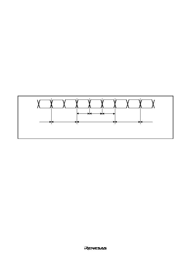
Rev. 2.0, 09/02, page 177 of 732
Bus Mode and Channel Priority Order
When a given channel is transferring in burst mode, and a transfer request is issued to channel 0,
which has a higher priority ranking, transfer on channel 0 begins immediately. If the priority level
setting is fixed mode (CH0
>
CH1), channel 1 transfer is continued after transfer on channel 0 are
completely ended, whether the channel 0 setting is cycle steal mode or burst mode.
When the priority level setting is for round robin mode, transfer on channel 1 begins after transfer
of one transfer unit on channel 0, whether channel 0 is set to cycle steal mode or burst mode.
Thereafter, bus mastership alternates in the order: channel 1
>
channel 0
>
channel 1
>
channel 0.
Whether the priority level setting is for fixed mode or round robin mode, since channel 1 is set to
burst mode, the bus mastership is not given to the CPU. An example of round robin mode is
shown in figure 10.13.
CPU
DMAC
CH1
DMAC
CH1
DMAC
CH0
DMAC
CH1
DMAC
CH0
DMAC
CH1
DMAC
CH1
CPU
CH0
CH1
CH0
DMAC CH0 and CH1
round-robin mode
DMAC CH1
burst mode
CPU
CPU
Priority: Round-robin mode
CH0: Cycle-steal mode
CH1: Burst mode
DMAC CH1
burst mode
Figure 10.13 Bus Handling when Multiple Channels Are Operating
10.4.5
Number of Bus Cycle States and
DREQ
DREQ
DREQ
DREQ Pin Sample Timing
Number of States in Bus Cycle: The number of states in the bus cycle when the DMAC is the
bus master is controlled by the bus state controller (BSC) just as it is when the CPU is the bus
master. For details, see section 9, Bus State Controller (BSC).
DREQ
DREQ
DREQ
DREQ Pin Sampling Timing and DRAK Signal: In external request mode, the DREQ pin is
sampled by either falling edge or low-level detection. When a
DREQ input is detected, a DMAC
bus cycle is issued and DMA transfer effected, at the earliest, after three states. However, in burst
mode when single address operation is specified, a dummy cycle is inserted for the first bus cycle.
In this case, the actual data transfer starts from the second bus cycle. Data is transferred
continuously from the second bus cycle. The dummy cycle is not counted in the number of
transfer cycles, so there is no need to recognize the dummy cycle when setting the TCR.
DREQ sampling from the second time begins from the start of the transfer one bus cycle prior to
the DMAC transfer generated by the previous sampling.
DRAK is output once for the first
DREQ sampling, irrespective of transfer mode or DREQ
detection method. In burst mode, using edge detection,
DREQ is sampled for the first cycle only,

Rev. 2.0, 09/02, page 178 of 732
so DRAK is also output for the first cycle only. Therefore, the
DREQ signal negate timing can be
ascertained, and this facilitates handshake operations of transfer requests with the DMAC.
Cycle Steal Mode Operations: In cycle steal mode,
DREQ sampling timing is the same
irrespective of dual or single address mode, or whether edge or low-level
DREQ detection is used.
For example, DMAC transfer begins (figure 10.14), at the earliest, three cycles from the first
sampling timing. The second sampling begins at the start of the transfer one bus cycle prior to the
start of the DMAC transfer initiated by the first sampling (i.e., from the start of the CPU(3)
transfer). At this point, if DREQ detection has not occurred, sampling is executed every cycle
thereafter.
As in figure 10.15, whatever cycle the CPU transfer cycle is, the next sampling begins from the
start of the transfer one bus cycle before the DMAC transfer begins.
Figure 10.14 shows an example of output during DACK read and figure 10.15 an example of
output during DACK write.
Figures 10.16 and 10.17 show cycle steal mode and single address mode. In this case, transfer
begins at earliest three cycles after the first
DREQ sampling. The second sampling begins from the
start of the transfer one bus cycle before the start of the first DMAC transfer. In single address
mode, the DACK signal is output during the DMAC transfer period.
Burst Mode, Dual Address, and Level Detection: Figures 10.18 and 10.19 show the
DREQ
sampling timing in burst mode with dual address and level detection.
DREQ sampling timing in
this mode is virtually the same as that of cycle steal mode.
For example, DMAC transfer begins (figure 10.18), at the earliest, three cycles after the timing of
the first sampling. The second sampling also begins from the start of the transfer one bus cycle
before the start of the first DMAC transfer. In burst mode, as long as transfer requests are issued,
DMAC transfer continues. Therefore, the "transfer one bus cycle before the start of the DMAC
transfer" may be a DMAC transfer.
In burst mode, the DACK output period is the same as that of cycle steal mode.
Burst Mode, Single Address, and Level Detection:
DREQ sampling timing in burst mode with
single address and level detection is shown in figures 10.20 and 10.21.
In burst mode with single address and level detection, a dummy cycle is inserted as one bus cycle,
at the earliest, three cycles after timing of the first sampling. Data during this period is undefined,
and the DACK signal is not output. Nor is the number of DMAC transfers counted. The actual
DMAC transfer begins after one dummy bus cycle output.

Rev. 2.0, 09/02, page 179 of 732
The dummy cycle is not counted either at the start of the second sampling (transfer one bus cycle
before the start of the first DMAC transfer). Therefore, the second sampling is not conducted from
the bus cycle starting the dummy cycle, but from the start of the CPU(3) bus cycle.
Thereafter, as long the
DREQ is continuously sampled, no dummy cycle is inserted. DREQ
sampling timing during this period begins from the start of the transfer one bus cycle before the
start of DMAC transfer, in the same way as with cycle steal mode.
As with the fourth sampling in figure 10.20, once DMAC transfer is interrupted, a dummy cycle is
again inserted at the start as soon as DMAC transfer is resumed.
The DACK output period in burst mode is the same as in cycle steal mode.
Burst Mode, Dual Address, and Edge Detection: In burst mode with dual address and edge
detection,
DREQ sampling is conducted only on the first cycle.
In figure 10.22, DMAC transfer begins, at the earliest, three cycles after the timing of the first
sampling. Thereafter, DMAC transfer continues until the end of the data transfer count set in the
DMATCR.
DREQ sampling is not conducted during this period. Therefore, DRAK is output on
the first cycle only.
When DMAC transfer is resumed after being halted by an NMI or address error, be sure to reinput
an edge request. The remaining transfer restarts after the first DRAK output.
The DACK output period in burst mode is the same as in cycle steal mode.
Burst Mode, Single Address, and Edge Detection: In burst mode with single address and edge
detection,
DREQ sampling is conducted only on the first cycle. In figure 10.23, a dummy cycle is
inserted, at the earliest, three cycles after the timing for the first sampling. During this period, data
is undefined, and DACK is not output. Nor is the number of DMAC transfers counted. Thereafter,
DMAC transfer continues until the data transfer count set in the DMATCR has ended.
DREQ
sampling is not conducted during this period. Therefore, DRAK is output on the first cycle only.
When DMAC transfer is resumed after being halted by an NMI or address error, be sure to reinput
an edge request. DRAK is output once, and the remaining transfer restarts after output of one
dummy cycle.
The DACK output period in burst mode is the same as in cycle steal mode.
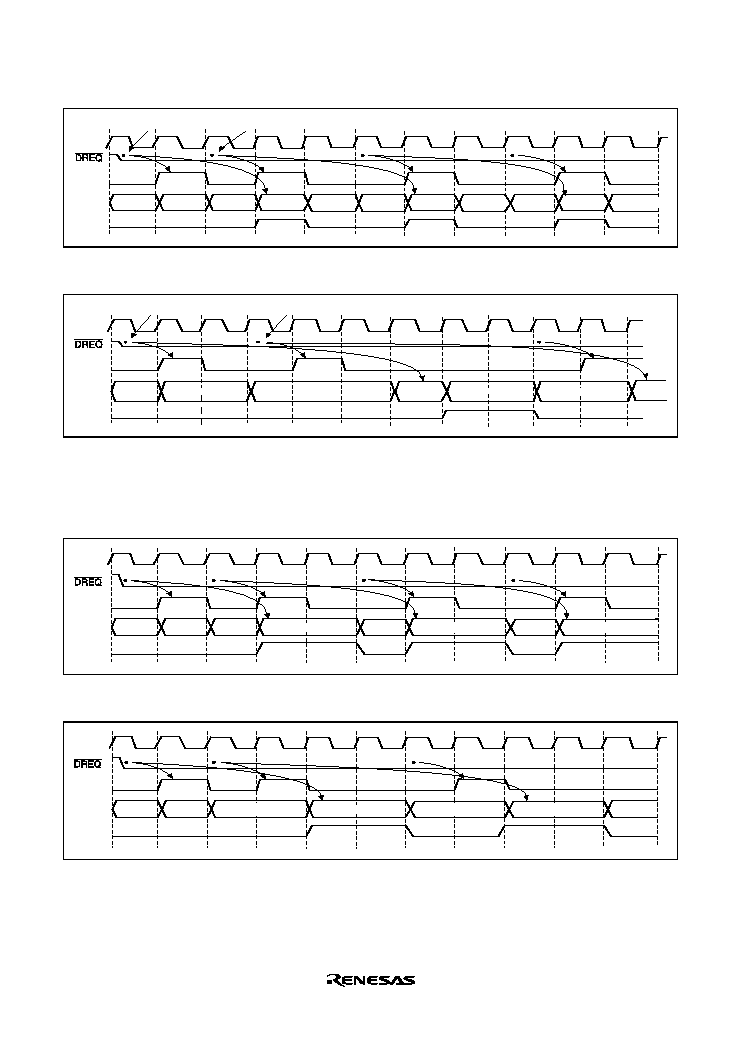
Rev. 2.0, 09/02, page 180 of 732
CK
DRAK
Bus
cycle
DACK
CPU(3)
CPU(4)
CPU(5)
CPU(2)
CPU(1)
1st sampling
2nd sampling
DMAC(R)
DMAC(R)
DMAC(W)
DMAC(W)
DMAC(W)
DMAC(R)
Figure 10.14 Cycle Steal, Dual Address and Level Detection (Fastest Operation)
CK
DRAK
Bus
cycle
DACK
CPU
CPU
CPU
CPU
DMAC(R)
DMAC
(R)
DMAC(W)
1st sampling
2nd sampling
Figure 10.15 Cycle Steal, Dual Address and Level Detection (Normal Operation)
Note:
With cycle-steal and dual address operation, sampling timing is the same regardless of
whether
DREQ detection is by level or by edge.
CK
DRAK
Bus
cycle
DACK
CPU
CPU
CPU
CPU
CPU
DMAC
DMAC
DMAC
Figure 10.16 Cycle Steal, Single Address and Level Detection (Fastest Operation)
CK
DRAK
Bus
cycle
DACK
CPU
CPU
DMAC
CPU
DMAC
CPU
CPU
Figure 10.17 Cycle Steal, Single Address and Level Detection (Normal Operation)
Note:
With cycle steal and single address operation, sampling timing is the same regardless of
whether
DREQ detection is by level or by edge.
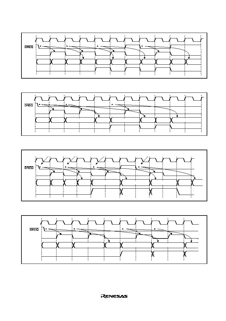
Rev. 2.0, 09/02, page 181 of 732
CK
DRAK
Bus
cycle
DACK
CPU
CPU
CPU
CPU
DMAC(R) DMAC(W)
DMAC(R)
DMAC(R)
DMAC(W)
DMAC(R)
DMAC(W)
Figure 10.18 Burst Mode, Dual Address and Level Detection (Fastest Operation)
CK
DRAK
Bus
cycle
DACK
CPU
CPU
DMAC(R)
DMAC(R)
DMAC(R)
CPU
DMAC(W)
DMAC(W)
Figure 10.19 Burst Mode, Dual Address and Level Detection (Normal Operation)
CK
DRAK
Bus
cycle
DACK
CPU(4)
CPU(1)
CPU(2)
CPU(3) Dummy
DMAC
Dummy
2nd sampling
1st sampling
3rd sampling
4th sampling
DMAC
DMAC
Figure 10.20 Burst Mode, Single Address and Level Detection (Fastest Operation)
CK
DRAK
Bus
cycle
DACK
CPU
CPU
Dummy
DMAC
CPU
DMAC
DMAC
Figure 10.21 Burst Mode, Single Address and Level Detection (Normal Operation)
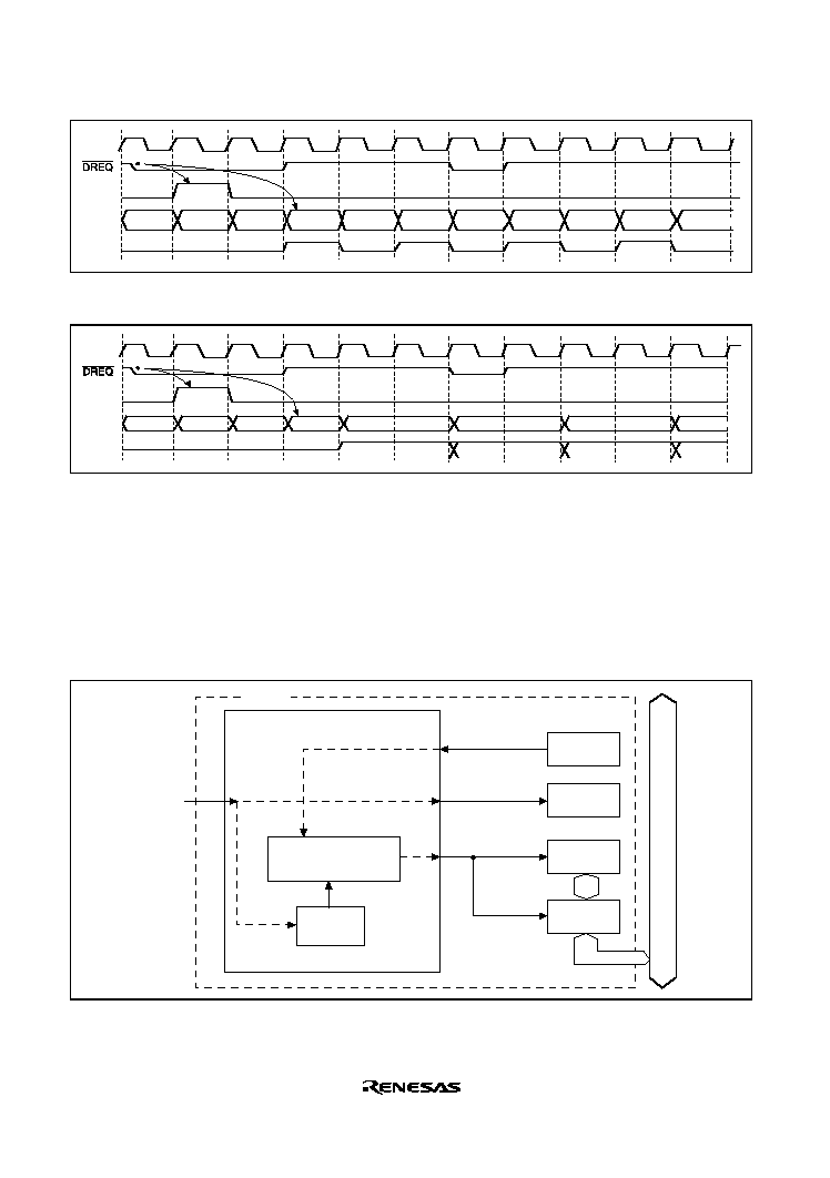
Rev. 2.0, 09/02, page 182 of 732
CK
DRAK
Bus
cycle
DACK
CPU
CPU
CPU
DMAC(R)
DMAC(R)
DMAC(R)
DMAC(R)
DMAC(W)
DMAC(W)
DMAC(W)
DMAC(W)
Figure 10.22 Burst Mode, Dual Address and Edge Detection
CK
DRAK
Bus
cycle
DACK
CPU
DMAC
DMAC
DMAC
DMAC
CPU
CPU
Dummy
Figure 10.23 Burst Mode, Single Address and Edge Detection
10.4.6
Source Address Reload Function
Channel 2 has a source address reload function. This returns to the first value set in the source
address register (SAR_2) every four transfers by setting the RO bit of CHCR_2 to 1. Figure 10.24
illustrates this operation. Figure 10.25 is a timing chart for reload ON mode, with burst mode,
autorequest, 16-bit transfer data size, SAR_2 increment, and DAR_2 fixed mode.
SAR_2
(initial value)
DMAC
Transfer
request
DMAC control block
Reload control
4th count
CHCR_2
DMATCR_2
SAR_2
RO bit = 1
Count signal
Reload
signal
Reload signal
Address b
u
s
Figure 10.24 Source Address Reload Function
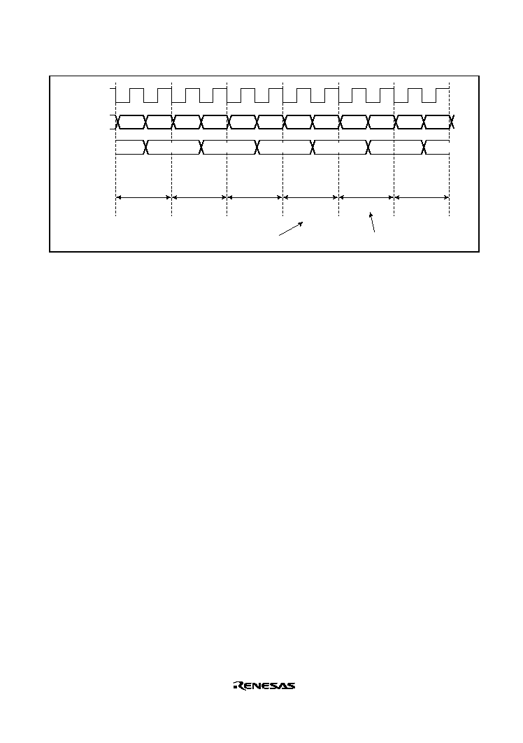
Rev. 2.0, 09/02, page 183 of 732
CK
Internal
address bus
Internal
data bus
SAR2
DAR2
DAR2
DAR2
DAR2
SAR2+2
SAR2+4
SAR2+6
SAR2
DAR2
SAR2 data
SAR2+2 data
SAR2+4 data
SAR2+6 data
SAR2 data
1st channel 2
transfer
2nd channel 2
transfer
3rd channel 2
transfer
4th channel 2
transfer
5th channel 2
transfer
SAR2 output
DAR2 output
SAR2+2 output
DAR2 output
SAR2+4 output
DAR2 output
SAR2+6 output
DAR2 output
SAR2 output
DAR2 output
After SAR2+6 output, SAR2 is reloaded
Bus mastership is returned one time in four
Figure 10.25 Source Address Reload Function Timing Chart
The reload function can be executed whether the transfer data size is 8, 16, or 32 bits.
DMATCR_2, which specifies the number of transfers, is decremented by 1 at the end of every
single-transfer-unit transfer, regardless of whether the reload function is on or off. Therefore,
when using the reload function in the on state, a multiple of 4 must be specified in DMATCR_2.
Operation will not be guaranteed if any other value is set. Also, the counter which counts the
occurrence of four transfers for address reloading is reset by clearing of the DME bit in DMAOR
or the DE bit in CHCR_2, setting of the transfer end flag (the TE bit in CHCR_2), NMI input, and
setting of the AE flag (address error generation in DMAC transfer), as well as by a reset and in
software standby mode, but SAR_2, DAR_2, DMATCR_2, and other registers are not reset.
Consequently, when one of these sources occurs, there is a mixture of initialized counters and
uninitialized registers in the DMAC, and incorrect operation may result if a restart is executed in
this state. Therefore, when one of the above sources, other than TE setting, occurs during use of
the address reload function, SAR_2, DAR_2, and DMATCR_2 settings must be carried out before
re-execution.

Rev. 2.0, 09/02, page 184 of 732
10.4.7
DMA Transfer Ending Conditions
The DMA transfer ending conditions vary for individual channels ending and for all channels
ending together.
Individual Channel Ending Conditions: There are two ending conditions. A transfer ends when
the value of the channel's DMA transfer count register (DMATCR) is 0, or when the DE bit of the
channel's CHCR is cleared to 0.
∑
When DMATCR is 0: When the DMATCR value becomes 0 and the corresponding channel's
DMA transfer ends, the transfer end flag bit (TE) is set in the CHCR. If the IE (interrupt
enable) bit has been set, a DMAC interrupt (DEI) is requested of the CPU.
∑
When DE of CHCR is 0: Software can halt a DMA transfer by clearing the DE bit in the
channel's CHCR. The TE bit is not set when this happens.
Conditions for Ending All Channels Simultaneously: Transfers on all channels end when the
NMIF (NMI flag) bit or AE (address error flag) bit is set to 1 in the DMAOR, or when the DME
bit in the DMAOR is cleared to 0.
∑
When the NMIF or AE bit is set to 1 in DMAOR: When an NMI interrupt or DMAC address
error occurs, the NMIF or AE bit is set to 1 in the DMAOR and all channels stop their
transfers. The DMAC obtains the bus mastership, and if these flags are set to 1 during
execution of a transfer, DMAC halts operation when the transfer processing currently being
executed ends, and transfers the bus mastership to the other bus master. Consequently, even if
the NMIF or AE bits are set to 1 during a transfer, the DMA source address register (SAR),
designation address register (DAR), and transfer count register (TCR) are all updated. The TE
bit is not set. To resume the transfers after NMI interrupt or address error processing, clear the
appropriate flag bit to 0. To avoid restarting a transfer on a particular channel, clear its DE bit
to 0.
Transfer is halted when the processing of a one unit transfer is complete. In a dual address
mode direct address transfer, even if an address error occurs or the NMI flag is set during read
processing, the transfer will not be halted until after completion of the following write
processing. In such a case, SAR, DAR, and TCR values are updated. In the same manner, the
transfer is not halted in dual address mode indirect address transfers until after the final write
processing has ended.
∑
When DME is cleared to 0 in DMAOR: Clearing the DME bit to 0 in the DMAOR aborts the
transfers on all channels. The TE bit is not set.

Rev. 2.0, 09/02, page 185 of 732
10.4.8
DMAC Access from CPU
The space addressed by the DMAC is 3-cycle space. Therefore, when the CPU becomes the bus
master and accesses the DMAC, a minimum of three system clock (
) cycles are required for one
bus cycle. Also, since the DMAC is located in word space, while a word-size access to the DMAC
is completed in one bus cycle, a longword-size access is automatically divided into two word
accesses, requiring two bus cycles (six basic clock cycles). These two bus cycles are executed
consecutively; a different bus cycle is never inserted between the two word accesses. This applies
to both write accesses and read accesses.
10.5
Examples of Use
10.5.1
Example of DMA Transfer between On-Chip SCI and External Memory
In this example, on-chip serial communication interface channel 0 (SCI0) received data is
transferred to external memory using the DMAC channel 3.
Table 10.6 indicates the transfer conditions and the setting values of each of the registers.
Table 10.6 Transfer Conditions and Register Set Values for Transfer between On-chip SCI
and External Memory
Transfer Conditions
Register
Value
Transfer source: RDR0 of on-chip SCI0
SAR_3
H'FFFF81A5
Transfer destination: external memory
DAR_3
H'00400000
Transfer count: 64 times
DMATCR_3
H'00000040
Transfer source address: fixed
CHCR_3
H'00004D05
Transfer destination address: incremented
Transfer request source: SCI0 (RDR0)
Bus mode: cycle steal
Transfer unit: byte
Interrupt request generation at end of transfer
Channel priority ranking: 0
>
1
>
2
>
3
DMAOR
H'0001

Rev. 2.0, 09/02, page 186 of 732
10.5.2
Example of DMA Transfer between External RAM and External Device with
DACK
In this example, an external request, single address mode transfer with external memory as the
transfer source and an external device with DACK as the transfer destination is executed using
DMAC channel 1.
Table 10.7 indicates the transfer conditions and the setting values of each of the registers.
Table 10.7 Transfer Conditions and Register Set Values for Transfer between External
RAM and External Device with DACK
Transfer Conditions
Register
Value
Transfer source: external RAM
SAR_1
H'00400000
Transfer destination: external device with DACK
DAR_1
(access by DACK)
Transfer count: 32 times
DMATCR_1
H'00000020
Transfer source address: decremented
CHCR_1
H'00002269
Transfer destination address: (setting ineffective)
Transfer request source: external pin (
DREQ1
) edge
detection
Bus mode: burst
Transfer unit: word
No interrupt request generation at end of transfer
Channel priority ranking: 2
>
0
>
1
>
3
DMAOR
H'0201
10.5.3
Example of DMA Transfer between A/D Converter and On-chip Memory (Address
Reload On)
In this example, the on-chip A/D converter channel 0 is the transfer source and on-chip memory is
the transfer destination, and the address reload function is on.
Table 10.8 indicates the transfer conditions and the setting values of each of the registers.

Rev. 2.0, 09/02, page 187 of 732
Table 10.8 Transfer Conditions and Register Set Values for Transfer between A/D
Converter (A/D1) and On-chip Memory
Transfer Conditions
Register
Value
Transfer source: on-chip A/D converter (A/D1)
SAR_2
H'FFFF8428
Transfer destination: on-chip memory
DAR_2
H'FFFFF000
Transfer count: 128 times (reload count 32 times)
DMATCR_2
H'00000080
Transfer source address: incremented
CHCR_2
H'00085B25
Transfer destination address: incremented
Transfer request source: A/D converter (A/D 1)
Bus mode: burst
Transfer unit: byte
Interrupt request generation at end of transfer
Channel priority ranking: 0
>
2
>
3
>
1
DMAOR
H'0101
When address reload is on, the SAR value returns to its initially established value every four
transfers. In the above example, when a transfer request is input from the A/D converter (A/D1),
the byte size data is first read from the H'FFFF8482 register of the A/D converter (AD1) and that
data is written to the on-chip memory address H'FFFFF000. Because a byte size transfer was
performed, the SAR and DAR values at this point are H'FFFF8429 and H'FFFFF001, respectively.
Also, because this is a burst transfer, the bus mastership remain secured, so continuous data
transfer is possible.
When four transfers are completed, if the address reload is off, execution continues with the fifth
and sixth transfers and the SAR value continues to increment from H'FFFF842B to H'FFFF842C
to H'FFFF842D and so on. However, when the address reload is on, the DMAC transfer is halted
upon completion of the fourth one and the bus mastership request signal to the CPU is cleared. At
this time, the value stored in SAR is not H'FFFF842B to H'FFFF842C, but H'FFFF842B to
H'FFFF8428, a return to the initially established address. The DAR value always continues to be
incremented regardless of whether the address reload is on or off.
The DMAC internal status, due to the above operation after completion of the fourth transfer, is
indicated in table 10.9 for both address reload on and off.

Rev. 2.0, 09/02, page 188 of 732
Table 10.9 DMAC Internal Status
Item
Address Reload On
Address Reload Off
SAR
H'FFFF8428
H'FFFF842C
DAR
H'FFFFF004
H'FFFFF004
DMATCR
H'0000007C
H'0000007C
Bus mastership
Released
Maintained
DMAC operation
Halted
Processing continues
Interrupts
Not issued
Not issued
Transfer request source flag clear
Executed
Not executed
Notes: 1. Interrupts are executed until the DMATCR value becomes 0, and if the IE bit of the
CHCR is set to 1, are issued regardless of whether the address reload is on or off.
2. If transfer request source flag clears are executed until the DMATCR value becomes 0,
they are executed regardless of whether the address reload is on or off.
3. Designate burst mode when using the address reload function. There are cases where
abnormal operation will result if it is executed in cycle steal mode.
4. Designate a multiple of four for the DMATCR value when using the address reload
function. There are cases where abnormal operation will result if anything else is
designated.
To execute transfers after the fifth one when the address reload is on, make the transfer request
source issue another transfer request signal.
10.5.4
Example of DMA Transfer between External Memory and SCI1 Transmit Side
(Indirect Address On)
In this example, DMAC channel 3 is used, an indirect address designated external memory is the
transfer source and the SCI1 transmit side is the transfer destination.
Table 10.10 indicates the transfer conditions and the setting values of each of the registers.

Rev. 2.0, 09/02, page 189 of 732
Table 10.10 Transfer Conditions and Register Set Values for Transfer between External
Memory and SCI1 Transmit Side
Transfer Conditions
Register
Value
Transfer source: external memory
SAR_3
H'00400000
Value stored in address H'00400000
--
H'00450000
Value stored in address H'00450000
--
H'55
Transfer destination: on-chip SCI1 (TDR1)
DAR_3
H'FFFF81B3
Transfer count: 10 times
DMATCR_3
H'0000000A
Transfer source address: incremented
CHCR_3
H'00011E01
Transfer destination address: fixed
Transfer request source: SCI1 (TDR1)
Bus mode: cycle steal
Transfer unit: byte
Interrupt request not generated at end of transfer
Channel priority ranking: 0
>
1
>
2
>
3
DMAOR
H'0001
When indirect address mode is on, the data stored in the address established in SAR is not used as
the transfer source data. In the case of indirect addressing, the value stored in the SAR address is
read, then that value is used as the address and the data read from that address is used as the
transfer source data, then that data is stored in the address designated by the DAR.
In the table 10.10 example, when a transfer request from the TDR_1 of SCI_1 is generated, a read
of the address located at H'00400000, which is the value set in SAR_3, is performed first. The data
H'00450000 is stored at this H'00400000 address, and the DMAC first reads this H'00450000
value. It then uses this read value of H'00450000 as an address and reads the value of H'55 that is
stored in the H'00450000 address. It then writes the value H'55 to the address H'FFFF81B3
designated by DAR_3 to complete one indirect address transfer.
With indirect addressing, the first executed data read from the address established in SAR_3
always results in a longword size transfer regardless of the TS0, TS1 bit designations for transfer
data size. However, the transfer source address fixed and increment or decrement designations are
as according to the SM0, SM1 bits. Consequently, despite the fact that the transfer data size
designation is byte in this example, the SAR_3 value at the end of one transfer is H'00400004. The
write operation is exactly the same as an ordinary dual address transfer write operation.

Rev. 2.0, 09/02, page 190 of 732
10.6
Cautions on Use
1. The DMA operation register (DMAOR) can be accessed only in word (16-bit) units. The other
registers can be accessed in word (16-bit) or longword (32-bit) units.
2. When rewriting the RS0 to RS3 bits of CHCR0 to CHCR3, first clear the DE bit to 0 (set the
DE bit to 0 before doing rewrites with CHCR).
3. When an NMI interrupt is input, the NMIF bit of the DMAOR is set even when the DMAC is
not operating.
4. Set the DME bit of the DMAOR to 0 and make certain that any DMAC received transfer
request processing has been completed before entering standby mode.
5. Do not access the DMAC, DTC, BSC, or UBC on-chip peripheral modules from the DMAC.
6. When activating the DMAC, do the CHCR or DMAOR setting as the final step. There are
instances where abnormal operation will result if any other registers are established last.
7. After the DMATCR count becomes 0 and the DMA transfer ends normally, always write a 0 to
the DMATCR, even when executing the maximum number of transfers on the same channel.
There are instances where abnormal operation will result if this is not done.
8. Designate burst mode as the transfer mode when using the address reload function. There are
instances where abnormal operation will result in cycle steal mode.
9. Designate a multiple of four for the DMATCR value when using the address reload function.
There are instances where abnormal operation will result if anything else is designated.
10. When detecting external requests by falling edge, maintain the external request pin at high
level when performing the DMAC establishment.
11. When operating in single address mode, establish an external address as the address. There are
instances where abnormal operation will result if an internal address is established.
12. Do not access DMAC register empty addresses (H'FFFF86B2 to H'FFFF86BF). Operation
cannot be guaranteed when empty addresses are accessed.

TIMMTU1A_010020020700
Rev. 2.0, 09/02, page 191 of 732
Section 11 Multi-Function Timer Pulse Unit (MTU)
This LSI has an on-chip multi-function timer pulse unit (MTU) that comprises five 16-bit timer
channels.
The block diagram is shown in figure 11.1.
11.1
Features
∑
Maximum 16-pulse input/output
∑
Selection of 8 counter input clocks for each channel
∑
The following operations can be set for each channel:
Waveform output at compare match
Input capture function
Counter clear operation
Multiple timer counters (TCNT) can be written to simultaneously
Simultaneous clearing by compare match and input capture is possible
Register simultaneous input/output is possible by synchronous counter operation
A maximum 12-phase PWM output is possible in combination with synchronous operation
∑
Buffer operation settable for channels 0, 3, and 4
∑
Phase counting mode settable independently for each of channels 1 and 2
∑
Cascade connection operation
∑
Fast access via internal 16-bit bus
∑
23 interrupt sources
∑
Automatic transfer of register data
∑
A/D converter conversion start trigger can be generated
∑
Module standby mode can be settable
∑
A total of six-phase waveform output, which includes complementary PWM output, and
positive and negative phases of reset PWM output by interlocking operation of channels 3 and
4, is possible.
∑
AC synchronous motor (brushless DC motor) drive mode using complementary PWM output
and reset PWM output is settable by interlocking operation of channels 0, 3, and 4, and the
selection of two types of waveform outputs (chopping and level) is possible.
Rev. 2.0, 09/02, page 192 of 732
Table 11.1 MTU Functions
Item
Channel 0
Channel 1
Channel 2
Channel 3
Channel 4
Count clock
P
/1
P
/4
P
/16
P
/64
TCLKA
TCLKB
TCLKC
TCLKD
P
/1
P
/4
P
/16
P
/64
P
/256
TCLKA
TCLKB
P
/1
P
/4
P
/16
P
/64
P
/1024
TCLKA
TCLKB
TCLKC
P
/1
P
/4
P
/16
P
/64
P
/256
P
/1024
TCLKA
TCLKB
P
/1
P
/4
P
/16
P
/64
P
/256
P
/1024
TCLKA
TCLKB
General registers
TGRA_0
TGRB_0
TGRA_1
TGRB_1
TGRA_2
TGRB_2
TGRA_3
TGRB_3
TGRA_4
TGRB_4
General registers/
buffer registers
TGRC_0
TGRD_0
--
--
TGRC_3
TGRD_3
TGRC_4
TGRD_4
I/O pins
TIOC0A
TIOC0B
TIOC0C
TIOC0D
TIOC1A
TIOC1B
TIOC2A
TIOC2B
TIOC3A
TIOC3B
TIOC3C
TIOC3D
TIOC4A
TIOC4B
TIOC4C
TIOC4D
Counter clear
function
TGR compare
match or input
capture
TGR compare
match or input
capture
TGR
compare
match or
input capture
TGR compare
match or input
capture
TGR
compare
match or
input capture
0
output
1
output
Compare
match
output
Toggle
output
Input capture
function
Synchronous
operation
PWM mode 1
PWM mode 2
--
--
Complementary
PWM mode
--
--
--
Reset PMW mode
--
--
--
AC synchronous
motor drive mode
--
--
Phase counting
mode
--
--
--

Rev. 2.0, 09/02, page 193 of 732
Item
Channel 0
Channel 1
Channel 2
Channel 3
Channel 4
Buffer operation
--
--
DMAC activation
TGRA_0
compare match
or input capture
TGRA_1
compare
match or
input capture
TGRA_2
compare
match or
input
capture
TGRA_3
compare
match or
input capture
TGRA_4
compare
match or
input
capture
DTC activation
TGR compare
match or input
capture
TGR
compare
match or
input capture
TGR
compare
match or
input
capture
TGR
compare
match or
input capture
TGR
compare
match or
input
capture and
TCNT
overflow or
underflow
A/D converter start
trigger
TGRA_0
compare match
or input capture
TGRA_1
compare
match or
input capture
TGRA_2
compare
match or
input
capture
TGRA_3
compare
match or
input capture
TGRA_4
compare
match or
input
capture
Interrupt sources
5 sources
∑
Compare
match or input
capture 0A
∑
Compare
match or input
capture 0B
∑
Compare
match or input
capture 0C
∑
Compare
match or input
capture 0D
∑
Overflow
4 sources
∑
Compare
match or
input
capture 1A
∑
Compare
match or
input
capture 1B
∑
Overflow
∑
Underflow
4 sources
∑
Compare
match or
input
capture 2A
∑
Compare
match or
input
capture 2B
∑
Overflow
∑
Underflow
5 sources
∑
Compare
match or
input
capture 3A
∑
Compare
match or
input
capture 3B
∑
Compare
match or
input
capture 3C
∑
Compare
match or
input
capture 3D
∑
Overflow
5 sources
∑
Compare
match or
input
capture 4A
∑
Compare
match or
input
capture 4B
∑
Compare
match or
input
capture 4C
∑
Compare
match or
input
capture 4D
∑
Overflow or
underflow
Legend:
: Possible
-- : Not possible
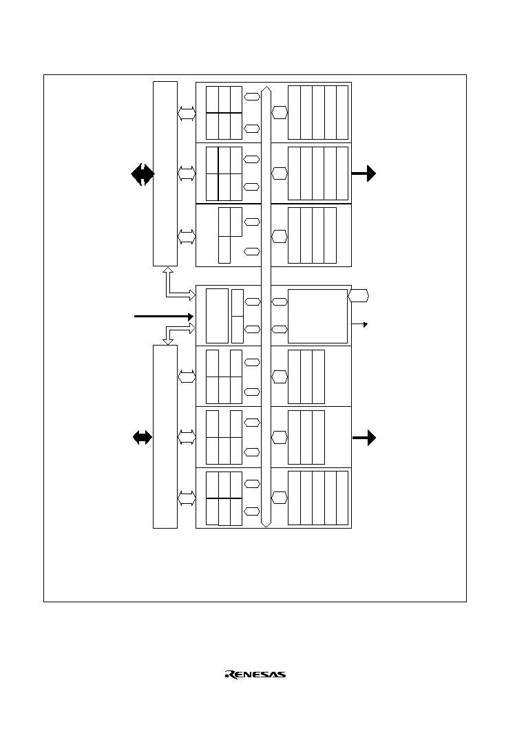
Rev. 2.0, 09/02, page 194 of 732
Internal data bus
A/D converter conversion
start signal
TCNT
TGRA
TGRB
TGRC
TGRD
TCR
TIORH
TIER
TMDR
TIORL
TSR
Channel 3
TCNT
TGRA
TGRB
TGRC
TGRD
TMDR
TIORL
TSR
TCR
TIORH
TIER
Channel 4
TCNTS
TCDR
TCBR
TDDR
TOER
TOCR
TGCR
BUS I/F
Common
TCNT
TGRA
TGRB
TMDR
TSR
TCR
TIOR
TIER
TSYR
TSTR
Channel 2
TCNT
TGRA
TGRB
TMDR
TSR
TCR
TIOR
TIER
Channel 1
TCNT
TGRA
TGRB
TGRC
TGRD
TMDR
TIORL
TSR
TCR
TIORH
TIER
Channel 0
Control logic
Module data bus
Control logic for channel 0 to 2
Control logic for channels 3 and 4
Legend:
TSTR:
TSYR:
TCR:
TMDR:
TIOR (H, L):
Timer start register
Timer synchro register
Timer control register
Timer mode register
Timer I/O control registers (H, L)
TIER:
TSR:
TCNT:
TGR (A, B, C, D):
Timer interrupt enable register
Timer status register
Timer counter
Timer general registers (A, B, C, D)
Interrupt request signals
Channel 3:
Channel 4:
TGIA_3
TGIB_3
TGIC_3
TGID_3
TCIV_3
TGIA_4
TGIB_4
TGIC_4
TGID_4
TCIV_4
Interrupt request signals
Channel 0:
Channel 1:
Channel 2:
TGIA_0
TGIB_0
TGIC_0
TGID_0
TCIV_0
TGIA_1
TGIB_1
TCIV_1
TCIU_1
TGIA_2
TGIB_2
TCIV_2
TCIU_2
TIOC0A
TIOC0B
TIOC0C
TIOC0D
TIOC1A
TIOC1B
TIOC2A
TIOC2B
Input/output pins
Channel 0:
Channel 1:
Channel 2:
P
/1
P
/4
P
/16
P
/64
P
/256
P
/1024
TCLKA
TCLKB
TCLKC
TCLKD
Clock input
Internal clock:
External clock:
TIOC3A
TIOC3B
TIOC3C
TIOC3D
TIOC4A
TIOC4B
TIOC4C
TIOC4D
Input/output pins
Channel 3:
Channel 4:
Figure 11.1 Block Diagram of MTU

Rev. 2.0, 09/02, page 195 of 732
11.2
Input/Output Pins
Table 11.2 MTU Pins
Channel
Symbol
I/O
Function
Common
TCLKA
Input
External clock A input pin
(Channel 1 phase counting mode A phase input)
TCLKB
Input
External clock B input pin
(Channel 1 phase counting mode B phase input)
TCLKC
Input
External clock C input pin
(Channel 2 phase counting mode A phase input)
TCLKD
Input
External clock D input pin
(Channel 2 phase counting mode B phase input)
0
TIOC0A
I/O
TGRA_0 input capture input/output compare output/PWM output pin
TIOC0B
I/O
TGRB_0 input capture input/output compare output/PWM output pin
TIOC0C
I/O
TGRC_0 input capture input/output compare output/PWM output pin
TIOC0D
I/O
TGRD_0 input capture input/output compare output/PWM output pin
1
TIOC1A
I/O
TGRA_1 input capture input/output compare output/PWM output pin
TIOC1B
I/O
TGRB_1 input capture input/output compare output/PWM output pin
2
TIOC2A
I/O
TGRA_2 input capture input/output compare output/PWM output pin
TIOC2B
I/O
TGRB_2 input capture input/output compare output/PWM output pin
3
TIOC3A
I/O
TGRA_3 input capture input/output compare output/PWM output pin
TIOC3B
I/O
TGRB_3 input capture input/output compare output/PWM output pin
TIOC3C
I/O
TGRC_3 input capture input/output compare output/PWM output pin
TIOC3D
I/O
TGRD_3 input capture input/output compare output/PWM output pin
4
TIOC4A
I/O
TGRA_4 input capture input/output compare output/PWM output pin
TIOC4B
I/O
TGRB_4 input capture input/output compare output/PWM output pin
TIOC4C
I/O
TGRC_4 input capture input/output compare output/PWM output pin
TIOC4D
I/O
TGRD_4 input capture input/output compare output/PWM output pin

Rev. 2.0, 09/02, page 196 of 732
11.3
Register Descriptions
The MTU has the following registers. For details on register addresses and register states during
each process, refer to section 25, List of Registers. To distinguish registers in each channel, an
underscore and the channel number are added as a suffix to the register name; TCR for channel 0
is expressed as TCR_0.
∑
Timer control register_0 (TCR_0)
∑
Timer mode register_0 (TMDR_0)
∑
Timer I/O control register H_0 (TIORH_0)
∑
Timer I/O control register L_0 (TIORL_0)
∑
Timer interrupt enable register_0 (TIER_0)
∑
Timer status register_0 (TSR_0)
∑
Timer counter_0 (TCNT_0)
∑
Timer general register A_0 (TGRA_0)
∑
Timer general register B_0 (TGRB_0)
∑
Timer general register C_0 (TGRC_0)
∑
Timer general register D_0 (TGRD_0)
∑
Timer control register_1 (TCR_1)
∑
Timer mode register_1 (TMDR_1)
∑
Timer I/O control register _1 (TIOR_1)
∑
Timer interrupt enable register_1 (TIER_1)
∑
Timer status register_1 (TSR_1)
∑
Timer counter_1 (TCNT_1)
∑
Timer general register A_1 (TGRA_1)
∑
Timer general register B_1 (TGRB_1)
∑
Timer control register_2 (TCR_2)
∑
Timer mode register_2 (TMDR_2)
∑
Timer I/O control register_2 (TIOR_2)
∑
Timer interrupt enable register_2 (TIER_2)
∑
Timer status register_2 (TSR_2)
∑
Timer counter_2 (TCNT_2)
∑
Timer general register A_2 (TGRA_2)
∑
Timer general register B_2 (TGRB_2)
∑
Timer control register_3 (TCR_3)
∑
Timer mode register_3 (TMDR_3)
∑
Timer I/O control register H_3 (TIORH_3)
∑
Timer I/O control register L_3 (TIORL_3)

Rev. 2.0, 09/02, page 197 of 732
∑
Timer interrupt enable register_3 (TIER_3)
∑
Timer status register_3 (TSR_3)
∑
Timer counter_3 (TCNT_3)
∑
Timer general register A_3 (TGRA_3)
∑
Timer general register B_3 (TGRB_3)
∑
Timer general register C_3 (TGRC_3)
∑
Timer general register D_3 (TGRD_3)
∑
Timer control register_4 (TCR_4)
∑
Timer mode register_4 (TMDR_4)
∑
Timer I/O control register H_4 (TIORH_4)
∑
Timer I/O control register L_4 (TIORL_4)
∑
Timer interrupt enable register_4 (TIER_4)
∑
Timer status register_4 (TSR_4)
∑
Timer counter_4 (TCNT_4)
∑
Timer general register A_4 (TGRA_4)
∑
Timer general register B_4 (TGRB_4)
∑
Timer general register C_4 (TGRC_4)
∑
Timer general register D_4 (TGRD_4)
Common Registers
∑
Timer start register (TSTR)
∑
Timer synchronous register (TSYR)
Common Registers for timers 3 and 4
∑
Timer output master enable register (TOER)
∑
Timer output control enable register (TOCR)
∑
Timer gate control register (TGCR)
∑
Timer cycle data register (TCDR)
∑
Timer dead time data register (TDDR)
∑
Timer subcounter (TCNTS)
∑
Timer cycle buffer register (TCBR)

Rev. 2.0, 09/02, page 198 of 732
11.3.1
Timer Control Register (TCR)
The TCR registers are 8-bit readable/writable registers that control the TCNT operation for each
channel. The MTU has a total of five TCR registers, one for each channel (channel 0 to 4). TCR
register settings should be conducted only when TCNT operation is stopped.
Bit
Bit Name
Initial value
R/W
Description
7
6
5
CCLR2
CCLR1
CCLR0
0
0
0
R/W
R/W
R/W
Counter Clear 0 to 2
These bits select the TCNT counter clearing source.
See tables 11.3 and 11.4 for details.
4
3
CKEG1
CKEG0
0
0
R/W
R/W
Clock Edge 0 and 1
These bits select the input clock edge. When the
input clock is counted using both edges, the input
clock period is halved (e.g. P
/4 both edges = P
/2
rising edge). If phase counting mode is used on
channels 1 and 2, this setting is ignored and the
phase counting mode setting has priority. Internal
clock edge selection is valid when the input clock is
P
/4 or slower. When P
/1, or the overflow/underflow
of another channel is selected for the input clock,
although values can be written, counter operation
compiles with the initial value.
00: Count at rising edge
01: Count at falling edge
1X: Count at both edges
Legend
X: Don't care
2
1
0
TPSC2
TPSC1
TPSC0
0
0
0
R/W
R/W
R/W
Time Prescaler 0 to 2
These bits select the TCNT counter clock. The clock
source can be selected independently for each
channel. See tables 11.5 to 11.8 for details.

Rev. 2.0, 09/02, page 199 of 732
Table 11.3 CCLR0 to CCLR2 (channels 0, 3, and 4)
Channel
Bit 7
CCLR2
Bit 6
CCLR1
Bit 5
CCLR0
Description
0, 3, 4
0
0
0
TCNT clearing disabled
1
TCNT cleared by TGRA compare match/input
capture
1
0
TCNT cleared by TGRB compare match/input
capture
1
TCNT cleared by counter clearing for another
channel performing synchronous clearing/
synchronous operation
*
1
1
0
0
TCNT clearing disabled
1
TCNT cleared by TGRC compare match/input
capture
*
2
1
0
TCNT cleared by TGRD compare match/input
capture
*
2
1
TCNT cleared by counter clearing for another
channel performing synchronous clearing/
synchronous operation
*
1
Notes: 1. Synchronous operation is set by setting the SYNC bit in TSYR to 1.
2. When TGRC or TGRD is used as a buffer register, TCNT is not cleared because the
buffer register setting has priority, and compare match/input capture does not occur.
Table 11.4 CCLR0 to CCLR2 (channels 1 and 2)
Channel
Bit 7
Reserved
*
2
Bit 6
CCLR1
Bit 5
CCLR0
Description
1, 2
0
0
0
TCNT clearing disabled
1
TCNT cleared by TGRA compare match/input
capture
1
0
TCNT cleared by TGRB compare match/input
capture
1
TCNT cleared by counter clearing for another
channel performing synchronous clearing/
synchronous operation
*
1
Notes: 1. Synchronous operation is selected by setting the SYNC bit in TSYR to 1.
2. Bit 7 is reserved in channels 1 and 2. It is always read as 0 and cannot be modified.

Rev. 2.0, 09/02, page 200 of 732
Table 11.5 TPSC0 to TPSC2 (channel 0)
Channel
Bit 2
TPSC2
Bit 1
TPSC1
Bit 0
TPSC0
Description
0
0
0
0
Internal clock: counts on P
/1
1
Internal clock: counts on P
/4
1
0
Internal clock: counts on P
/16
1
Internal clock: counts on P
/64
1
0
0
External clock: counts on TCLKA pin input
1
External clock: counts on TCLKB pin input
1
0
External clock: counts on TCLKC pin input
1
External clock: counts on TCLKD pin input
Table 11.6 TPSC0 to TPSC2 (channel 1)
Channel
Bit 2
TPSC2
Bit 1
TPSC1
Bit 0
TPSC0
Description
1
0
0
0
Internal clock: counts on P
/1
1
Internal clock: counts on P
/4
1
0
Internal clock: counts on P
/16
1
Internal clock: counts on P
/64
1
0
0
External clock: counts on TCLKA pin input
1
External clock: counts on TCLKB pin input
1
0
Internal clock: counts on P
/256
1
Counts on TCNT_2 overflow/underflow
Note:
This setting is ignored when channel 1 is in phase counting mode.

Rev. 2.0, 09/02, page 201 of 732
Table 11.7 TPSC0 to TPSC2 (channel 2)
Channel
Bit 2
TPSC2
Bit 1
TPSC1
Bit 0
TPSC0
Description
2
0
0
0
Internal clock: counts on P
/1
1
Internal clock: counts on P
/4
1
0
Internal clock: counts on P
/16
1
Internal clock: counts on P
/64
1
0
0
External clock: counts on TCLKA pin input
1
External clock: counts on TCLKB pin input
1
0
External clock: counts on TCLKC pin input
1
Internal clock: counts on P
/1024
Note:
This setting is ignored when channel 2 is in phase counting mode.
Table 11.8 TPSC0 to TPSC2 (channels 3 and 4)
Channel
Bit 2
TPSC2
Bit 1
TPSC1
Bit 0
TPSC0
Description
3, 4
0
0
0
Internal clock: counts on P
/1
1
Internal clock: counts on P
/4
1
0
Internal clock: counts on P
/16
1
Internal clock: counts on P
/64
1
0
0
Internal clock: counts on P
/256
1
Internal clock: counts on P
/1024
1
0
External clock: counts on TCLKA pin input
1
External clock: counts on TCLKB pin input

Rev. 2.0, 09/02, page 202 of 732
11.3.2
Timer Mode Register (TMDR)
The TMDR registers are 8-bit readable/writable registers that are used to set the operating mode of
each channel. The MTU has five TMDR registers, one for each channel. TMDR register settings
should be changed only when TCNT operation is stopped.
Bit
Bit Name
Initial value
R/W
Description
7
6
--
--
1
1
--
--
Reserved
These bits are always read as 1 and should be
written with 1.
5
BFB
0
R/W
Buffer Operation B
Specifies whether TGRB is to operate in the normal
way, or TGRB and TGRD are to be used together for
buffer operation. When TGRD is used as a buffer
register, TGRD input capture/output compare is not
generated.
In channels 1 and 2, which have no TGRD, bit 5 is
reserved. It is always read as 0 and cannot be
modified.
0: TGRB and TGRD operate normally
1: TGRB and TGRD used together for buffer
operation
4
BFA
0
R/W
Buffer Operation A
Specifies whether TGRA is to operate in the normal
way, or TGRA and TGRC are to be used together for
buffer operation. When TGRC is used as a buffer
register, TGRC input capture/output compare is not
generated.
In channels 1 and 2, which have no TGRC, bit 4 is
reserved. It is always read as 0 and cannot be
modified.
0: TGRA and TGRC operate normally
1: TGRA and TGRC used together for buffer
operation
3
2
1
0
MD3
MD2
MD1
MD0
0
0
0
0
R/W
R/W
R/W
R/W
Modes 0 to 3
These bits are used to set the timer operating mode.
See table 11.9 for details.

Rev. 2.0, 09/02, page 203 of 732
Table 11.9 MD0 to MD3
Bit 3
MD3
Bit 2
MD2
Bit 1
MD1
Bit 0
MD0
Description
0
0
0
0
Normal operation
1
Setting prohibited
1
0
PWM mode 1
1
PWM mode 2
*
1
1
0
0
Phase counting mode 1
*
2
1
Phase counting mode 2
*
2
1
0
Phase counting mode 3
*
2
1
Phase counting mode 4
*
2
1
0
0
0
Reset synchronous PWM mode
*
3
1
Setting prohibited
1
X
Setting prohibited
1
0
0
Setting prohibited
1
Complementary PWM mode 1 (transmit at peak)
*
3
1
0
Complementary PWM mode 2 (transmit at valley)
*
3
1
Complementary PWM mode 2 (transmit at peak and valley)
*
3
Legend:
X: Don't care
Notes: 1. PWM mode 2 can not be set for channels 3, 4.
2. Phase counting mode can not be set for channels 0, 3, 4.
3. Reset synchronous PWM mode, complementary PWM mode can only be set for
channel 3. When channel 3 is set to reset synchronous PWM mode or complementary
PWM mode, the channel 4 settings become ineffective and automatically conform to the
channel 3 settings. However, do not set channel 4 to reset synchronous PWM mode or
complementary PWM mode. Reset synchronous PWM mode and complementary PWM
mode can not be set for channels 0, 1, 2.
11.3.3
Timer I/O Control Register (TIOR)
The TIOR registers are 8-bit readable/writable registers that control the TGR registers. The MTU
has eight TIOR registers, two each for channels 0, 3, and 4, and one each for channels 1 and 2.
Care is required as TIOR is affected by the TMDR setting. The initial output specified by TIOR is
valid when the counter is stopped (the CST bit in TSTR is cleared to 0). Note also that, in PWM
mode 2, the output at the point at which the counter is cleared to 0 is specified.
When TGRC or TGRD is designated for buffer operation, this setting is invalid and the register
operates as a buffer register.

Rev. 2.0, 09/02, page 204 of 732
TIORH_0, TIOR_1, TIOR_2, TIORH_3, TIORH_4
Bit
Bit Name
Initial value
R/W
Description
7
6
5
4
IOB3
IOB2
IOB1
IOB0
0
0
0
0
R/W
R/W
R/W
R/W
I/O Control B0 to B3
Specify the function of TGRB.
See the following tables.
TIORH_0: Table 11.10
TIOR_1:
Table 11.12
TIOR_2:
Table 11.13
TIORH_3: Table 11.14
TIORH_4: Table 11.16
3
2
1
0
IOA3
IOA2
IOA1
IOA0
0
0
0
0
R/W
R/W
R/W
R/W
I/O Control A0 to A3
Specify the function of TGRA.
See the following tables.
TIORH_0: Table 11.18
TIOR_1:
Table 11.20
TIOR_2:
Table 11.21
TIORH_3: Table 11.22
TIORH_4: Table 11.24
TIORL_0, TIORL_3, TIORL_4
Bit
Bit Name
Initial value
R/W
Description
7
6
5
4
IOD3
IOD2
IOD1
IOD0
0
0
0
0
R/W
R/W
R/W
R/W
I/O Control D0 to D3
Specify the function of TGRD.
See the following tables.
TIORL_0: Table 11.11
TIORL_3: Table 11.15
TIORL_4: Table 11.17
3
2
1
0
IOC3
IOC2
IOC1
IOC0
0
0
0
0
R/W
R/W
R/W
R/W
I/O Control C0 to C3
Specify the function of TGRC.
See the following tables.
TIORL_0: Table 11.19
TIORL_3: Table 11.23
TIORL_4: Table 11.25

Rev. 2.0, 09/02, page 205 of 732
Table 11.10 TIORH_0 (channel 0)
Description
Bit 7
IOB3
Bit 6
IOB2
Bit 5
IOB1
Bit 4
IOB0
TGRB_0
Function
TIOC0B Pin Function
0
Output retained
*
0
1
Initial output is 0
0 output at compare match
0
Initial output is 0
1 output at compare match
0
1
1
Initial output is 0
Toggle output at compare match
0
0
Output retained
1
Initial output is 1
0 output at compare match
0
Initial output is 1
1 output at compare match
0
1
1
1
Output
compare
register
Initial output is 1
Toggle output at compare match
0
Input capture at rising edge
0
1
Input capture at falling edge
0
1
X
Input capture at both edges
1
1
X
X
Input
capture
register
Capture input source is channel 1/count clock
Input capture at TCNT_1 count- up/count-down
Legend:
X: Don't care
Note:
*
After power-on reset, 0 is output until TIOR is set.

Rev. 2.0, 09/02, page 206 of 732
Table 11.11 TIORL_0 (channel 0)
Description
Bit 7
IOD3
Bit 6
IOD2
Bit 5
IOD1
Bit 4
IOD0
TGRD_0
Function
TIOC0D Pin Function
0
0
0
0
Output retained
*
1
1
Initial output is 0
0 output at compare match
1
0
Output
compare
register
*
2
Initial output is 0
1 output at compare match
1
Initial output is 0
Toggle output at compare match
1
0
0
Output retained
1
Initial output is 1
0 output at compare match
1
0
Initial output is 1
1 output at compare match
1
Initial output is 1
Toggle output at compare match
1
0
0
0
Input capture at rising edge
1
Input capture at falling edge
1
X
Input capture at both edges
1
X
X
Input
capture
register
*
2
Capture input source is channel 1/count clock
Input capture at TCNT_1 count-up/count-down
Legend:
X: Don't care
Notes: 1. After power-on reset, 0 is output until TIOR is set.
2. When the BFB bit in TMDR_0 is set to 1 and TGRD_0 is used as a buffer register, this
setting is invalid and input capture/output compare is not generated.

Rev. 2.0, 09/02, page 207 of 732
Table 11.12 TIOR_1 (channel 1)
Description
Bit 7
IOB3
Bit 6
IOB2
Bit 5
IOB1
Bit 4
IOB0
TGRB_1
Function
TIOC1B Pin Function
0
0
0
0
Output retained
*
1
Output
compare
register
Initial output is 0
0 output at compare match
1
0
Initial output is 0
1 output at compare match
1
Initial output is 0
Toggle output at compare match
1
0
0
Output retained
1
Initial output is 1
0 output at compare match
1
0
Initial output is 1
1 output at compare match
1
Initial output is 1
Toggle output at compare match
1
0
0
0
Input capture at rising edge
1
Input capture at falling edge
1
X
Input capture at both edges
1
X
X
Input
capture
register
Input capture at generation of TGRC_0 compare
match/input capture
Legend:
X: Don't care
Note:
*
After power-on reset, 0 is output until TIOR is set.

Rev. 2.0, 09/02, page 208 of 732
Table 11.13 TIOR_2 (channel 2)
Description
Bit 7
IOB3
Bit 6
IOB2
Bit 5
IOB1
Bit 4
IOB0
TGRB_2
Function
TIOC2B Pin Function
0
0
0
0
Output retained
*
1
Output
compare
register
Initial output is 0
0 output at compare match
1
0
Initial output is 0
1 output at compare match
1
Initial output is 0
Toggle output at compare match
1
0
0
Output retained
1
Initial output is 1
0 output at compare match
1
0
Initial output is 1
1 output at compare match
1
Initial output is 1
Toggle output at compare match
1
X
0
0
Input capture at rising edge
1
Input capture at falling edge
1
X
Input
capture
register
Input capture at both edges
Legend:
X: Don't care
Note:
*
After power-on reset, 0 is output until TIOR is set.

Rev. 2.0, 09/02, page 209 of 732
Table 11.14 TIORH_3 (channel 3)
Description
Bit 7
IOB3
Bit 6
IOB2
Bit 5
IOB1
Bit 4
IOB0
TGRB_3
Function
TIOC3B Pin Function
0
0
0
0
Output retained
*
1
Output
compare
register
Initial output is 0
0 output at compare match
1
0
Initial output is 0
1 output at compare match
1
Initial output is 0
Toggle output at compare match
1
0
0
Output retained
1
Initial output is 1
0 output at compare match
1
0
Initial output is 1
1 output at compare match
1
Initial output is 1
Toggle output at compare match
1
X
0
0
Input capture at rising edge
1
Input capture at falling edge
1
X
Input
capture
register
Input capture at both edges
Legend:
X: Don't care
Note:
*
After power-on reset, 0 is output until TIOR is set.

Rev. 2.0, 09/02, page 210 of 732
Table 11.15 TIORL_3 (channel 3)
Description
Bit 7
IOD3
Bit 6
IOD2
Bit 5
IOD1
Bit 4
IOD0
TGRD_3
Function
TIOC3D Pin Function
0
0
0
0
Output retained
*
1
1
Output
compare
register
*
2
Initial output is 0
0 output at compare match
1
0
Initial output is 0
1 output at compare match
1
Initial output is 0
Toggle output at compare match
1
0
0
Output retained
1
Initial output is 1
0 output at compare match
1
0
Initial output is 1
1 output at compare match
1
Initial output is 1
Toggle output at compare match
1
X
0
0
Input capture at rising edge
1
Input capture at falling edge
1
X
Input
capture
register
*
2
Input capture at both edges
Legend:
X: Don't care
Notes: 1. After power-on reset, 0 is output until TIOR is set.
2. When the BFB bit in TMDR_3 is set to 1 and TGRD_3 is used as a buffer register, this
setting is invalid and input capture/output compare is not generated.

Rev. 2.0, 09/02, page 211 of 732
Table 11.16 TIORH_4 (channel 4)
Description
Bit 7
IOB3
Bit 6
IOB2
Bit 5
IOB1
Bit 4
IOB0
TGRB_4
Function
TIOC4B Pin Function
0
0
0
0
Output retained
*
1
Output
compare
register
Initial output is 0
0 output at compare match
1
0
Initial output is 0
1 output at compare match
1
Initial output is 0
Toggle output at compare match
1
0
0
Output retained
1
Initial output is 1
0 output at compare match
1
0
Initial output is 1
1 output at compare match
1
Initial output is 1
Toggle output at compare match
1
X
0
0
Input capture at rising edge
1
Input capture at falling edge
1
X
Input
capture
register
Input capture at both edges
Legend:
X: Don't care
Note:
*
After power-on reset, 0 is output until TIOR is set.

Rev. 2.0, 09/02, page 212 of 732
Table 11.17 TIORL_4 (channel 4)
Description
Bit 7
IOD3
Bit 6
IOD2
Bit 5
IOD1
Bit 4
IOD0
TGRD_4
Function
TIOC4D Pin Function
0
0
0
0
Output retained
*
1
1
Output
compare
register
*
2
Initial output is 0
0 output at compare match
1
0
Initial output is 0
1 output at compare match
1
Initial output is 0
Toggle output at compare match
1
0
0
Output retained
1
Initial output is 1
0 output at compare match
1
0
Initial output is 1
1 output at compare match
1
Initial output is 1
Toggle output at compare match
1
X
0
0
Input capture at rising edge
1
Input capture at falling edge
1
X
Input
capture
register
*
2
Input capture at both edges
Legend:
X: Don't care
Notes: 1. After power-on reset, 0 is output until TIOR is set.
2. When the BFB bit in TMDR_4 is set to 1 and TGRD_4 is used as a buffer register, this
setting is invalid and input capture/output compare is not generated.

Rev. 2.0, 09/02, page 213 of 732
Table 11.18 TIORH_0 (channel 0)
Description
Bit 3
IOA3
Bit 2
IOA2
Bit 1
IOA1
Bit 0
IOA0
TGRA_0
Function
TIOC0A Pin Function
0
0
0
0
Output retained
*
1
Output
compare
register
Initial output is 0
0 output at compare match
1
0
Initial output is 0
1 output at compare match
1
Initial output is 0
Toggle output at compare match
1
0
0
Output retained
1
Initial output is 1
0 output at compare match
1
0
Initial output is 1
1 output at compare match
1
Initial output is 1
Toggle output at compare match
1
0
0
0
Input capture at rising edge
1
Input capture at falling edge
1
X
Input capture at both edges
1
X
X
Input
capture
register
Capture input source is channel 1/count clock
Input capture at TCNT_1 count-up/count-down
Legend:
X: Don't care
Note:
*
After power-on reset, 0 is output until TIOR is set.

Rev. 2.0, 09/02, page 214 of 732
Table 11.19 TIORL_0 (channel 0)
Description
Bit 3
IOC3
Bit 2
IOC2
Bit 1
IOC1
Bit 0
IOC0
TGRC_0
Function
TIOC0C Pin Function
0
0
0
0
Output retained
*
1
1
Output
compare
register
*
2
Initial output is 0
0 output at compare match
1
0
Initial output is 0
1 output at compare match
1
Initial output is 0
Toggle output at compare match
1
0
0
Output retained
1
Initial output is 1
0 output at compare match
1
0
Initial output is 1
1 output at compare match
1
Initial output is 1
Toggle output at compare match
1
0
0
0
Input capture at rising edge
1
Input capture at falling edge
1
X
Input capture at both edges
1
X
X
Input
capture
register
*
2
Capture input source is channel 1/count clock
Input capture at TCNT_1 count-up/count-down
Legend:
X: Don't care
Notes: 1. After power-on reset, 0 is output until TIOR is set.
2. When the BFA bit in TMDR_0 is set to 1 and TGRC_0 is used as a buffer register, this
setting is invalid and input capture/output compare is not generated.

Rev. 2.0, 09/02, page 215 of 732
Table 11.20 TIOR_1 (channel 1)
Description
Bit 3
IOA3
Bit 2
IOA2
Bit 1
IOA1
Bit 0
IOA0
TGRA_1
Function
TIOC1A Pin Function
0
0
0
0
Output retained
*
1
Output
compare
register
Initial output is 0
0 output at compare match
1
0
Initial output is 0
1 output at compare match
1
Initial output is 0
Toggle output at compare match
1
0
0
Output retained
1
Initial output is 1
0 output at compare match
1
0
Initial output is 1
1 output at compare match
1
Initial output is 1
Toggle output at compare match
1
0
0
0
Input capture at rising edge
1
Input capture at falling edge
1
X
Input capture at both edges
1
X
X
Input
capture
register
Input capture at generation of channel 0/TGRA_0
compare match/input capture
Legend:
X: Don't care
Note:
*
After power-on reset, 0 is output until TIOR is set.

Rev. 2.0, 09/02, page 216 of 732
Table 11.21 TIOR_2 (channel 2)
Description
Bit 3
IOA3
Bit 2
IOA2
Bit 1
IOA1
Bit 0
IOA0
TGRA_2
Function
TIOC2A Pin Function
0
0
0
0
Output retained
*
1
Output
compare
register
Initial output is 0
0 output at compare match
1
0
Initial output is 0
1 output at compare match
1
Initial output is 0
Toggle output at compare match
1
0
0
Output retained
1
Initial output is 1
0 output at compare match
1
0
Initial output is 1
1 output at compare match
1
Initial output is 1
Toggle output at compare match
1
X
0
0
Input capture at rising edge
1
Input capture at falling edge
1
X
Input
capture
register
Input capture at both edges
Legend:
X: Don't care
Note:
*
After power-on reset, 0 is output until TIOR is set.

Rev. 2.0, 09/02, page 217 of 732
Table 11.22 TIORH_3 (channel 3)
Description
Bit 3
IOA3
Bit 2
IOA2
Bit 1
IOA1
Bit 0
IOA0
TGRA_3
Function
TIOC3A Pin Function
0
0
0
0
Output retained
*
1
Output
compare
register
Initial output is 0
0 output at compare match
1
0
Initial output is 0
1 output at compare match
1
Initial output is 0
Toggle output at compare match
1
0
0
Output retained
1
Initial output is 1
0 output at compare match
1
0
Initial output is 1
1 output at compare match
1
Initial output is 1
Toggle output at compare match
1
X
0
0
Input capture at rising edge
1
Input capture at falling edge
1
X
Input
capture
register
Input capture at both edges
Legend:
X: Don't care
Note:
*
After power-on reset, 0 is output until TIOR is set.

Rev. 2.0, 09/02, page 218 of 732
Table 11.23 TIORL_3 (channel 3)
Description
Bit 3
IOC3
Bit 2
IOC2
Bit 1
IOC1
Bit 0
IOC0
TGRC_3
Function
TIOC3C Pin Function
0
0
0
0
Output retained
*
1
1
Output
compare
register
*
2
Initial output is 0
0 output at compare match
1
0
Initial output is 0
1 output at compare match
1
Initial output is 0
Toggle output at compare match
1
0
0
Output retained
1
Initial output is 1
0 output at compare match
1
0
Initial output is 1
1 output at compare match
1
Initial output is 1
Toggle output at compare match
1
X
0
0
Input capture at rising edge
1
Input capture at falling edge
1
X
Input
capture
register
*
2
Input capture at both edges
Legend:
X: Don't care
Notes: 1. After power-on reset, 0 is output until TIOR is set.
2. When the BFA bit in TMDR_3 is set to 1 and TGRC_3 is used as a buffer register, this
setting is invalid and input capture/output compare is not generated.

Rev. 2.0, 09/02, page 219 of 732
Table 11.24 TIORH_4 (channel 4)
Description
Bit 3
IOA3
Bit 2
IOA2
Bit 1
IOA1
Bit 0
IOA0
TGRA_4
Function
TIOC4A Pin Function
0
0
0
0
Output retained
*
1
Output
compare
register
Initial output is 0
0 output at compare match
1
0
Initial output is 0
1 output at compare match
1
Initial output is 0
Toggle output at compare match
1
0
0
Output retained
1
Initial output is 1
0 output at compare match
1
0
Initial output is 1
1 output at compare match
1
Initial output is 1
Toggle output at compare match
1
X
0
0
Input capture at rising edge
1
Input capture at falling edge
1
X
Input
capture
register
Input capture at both edges
Legend:
X: Don't care
Note:
*
After power-on reset, 0 is output until TIOR is set.

Rev. 2.0, 09/02, page 220 of 732
Table 11.25 TIORL_4 (channel 4)
Description
Bit 3
IOC3
Bit 2
IOC2
Bit 1
IOC1
Bit 0
IOC0
TGRC_4
Function
TIOC4C Pin Function
0
0
0
0
Output retained
*
1
1
Output
compare
register
*
2
Initial output is 0
0 output at compare match
1
0
Initial output is 0
1 output at compare match
1
Initial output is 0
Toggle output at compare match
1
0
0
Output retained
1
Initial output is 1
0 output at compare match
1
0
Initial output is 1
1 output at compare match
1
Initial output is 1
Toggle output at compare match
1
X
0
0
Input capture at rising edge
1
Input capture at falling edge
1
X
Input
capture
register
*
2
Input capture at both edges
Legend:
X: Don't care
Notes: 1. After power-on reset, 0 is output until TIOR is set.
2. When the BFA bit in TMDR_4 is set to 1 and TGRC_4 is used as a buffer register, this
setting is invalid and input capture/output compare is not generated.

Rev. 2.0, 09/02, page 221 of 732
11.3.4
Timer Interrupt Enable Register (TIER)
The TIER registers are 8-bit readable/writable registers that control enabling or disabling of
interrupt requests for each channel. The MTU has five TIER registers, one for each channel.
Bit
Bit Name
Initial value
R/W
Description
7
TTGE
0
R/W
A/D Conversion Start Request Enable
Enables or disables generation of A/D conversion
start requests by TGRA input capture/compare
match.
0: A/D conversion start request generation disabled
1: A/D conversion start request generation enabled
6
--
1
R
Reserved
This bit is always read as 1 and should be written with
1.
5
TCIEU
0
R/W
Underflow Interrupt Enable
Enables or disables interrupt requests (TCIU) by the
TCFU flag when the TCFU flag in TSR is set to 1 in
channels 1 and 2.
In channels 0, 3, and 4, bit 5 is reserved. It is always
read as 0 and should be written with 0.
0: Interrupt requests (TCIU) by TCFU disabled
1: Interrupt requests (TCIU) by TCFU enabled
4
TCIEV
0
R/W
Overflow Interrupt Enable
Enables or disables interrupt requests (TCIV) by the
TCFV flag when the TCFV flag in TSR is set to 1.
0: Interrupt requests (TCIV) by TCFV disabled
1: Interrupt requests (TCIV) by TCFV enabled
3
TGIED
0
R/W
TGR Interrupt Enable D
Enables or disables interrupt requests (TGID) by the
TGFD bit when the TGFD bit in TSR is set to 1 in
channels 0, 3, and 4.
In channels 1 and 2, bit 3 is reserved. It is always
read as 0 and should be written with 0.
0: Interrupt requests (TGID) by TGFD bit disabled
1: Interrupt requests (TGID) by TGFD bit enabled

Rev. 2.0, 09/02, page 222 of 732
Bit
Bit Name
Initial value
R/W
Description
2
TGIEC
0
R/W
TGR Interrupt Enable C
Enables or disables interrupt requests (TGIC) by the
TGFC bit when the TGFC bit in TSR is set to 1 in
channels 0, 3, and 4.
In channels 1 and 2, bit 2 is reserved. It is always
read as 0 and should be written with 0.
0: Interrupt requests (TGIC) by TGFC bit disabled
1: Interrupt requests (TGIC) by TGFC bit enabled
1
TGIEB
0
R/W
TGR Interrupt Enable B
Enables or disables interrupt requests (TGIB) by the
TGFB bit when the TGFB bit in TSR is set to 1.
0: Interrupt requests (TGIB) by TGFB bit disabled
1: Interrupt requests (TGIB) by TGFB bit enabled
0
TGIEA
0
R/W
TGR Interrupt Enable A
Enables or disables interrupt requests (TGIA) by the
TGFA bit when the TGFA bit in TSR is set to 1.
0: Interrupt requests (TGIA) by TGFA bit disabled
1: Interrupt requests (TGIA) by TGFA bit enabled

Rev. 2.0, 09/02, page 223 of 732
11.3.5
Timer Status Register (TSR)
The TSR registers are 8-bit readable/writable registers that indicate the status of each channel. The
MTU has five TSR registers, one for each channel.
Bit
Bit Name Initial value R/W
Description
7
TCFD
1
R
Count Direction Flag
Status flag that shows the direction in which TCNT
counts in channels 1, 2, 3, and 4.
In channel 0, bit 7 is reserved. It is always read as 1 and
should be written with 1.
0: TCNT counts down
1: TCNT counts up
6
--
1
R
Reserved
This bit is always read as 1 and should be written with 1.
5
TCFU
0
R/(W)
*
Underflow Flag
Status flag that indicates that TCNT underflow has
occurred when channels 1 and 2 are set to phase
counting mode. Only 0 can be written, for flag clearing.
In channels 0, 3, and 4, bit 5 is reserved. It is always
read as 0 and should be written with 0.
[Setting condition]
∑
When the TCNT value underflows (changes from
H'0000 to H'FFFF)
[Clearing condition]
∑
When 0 is written to TCFU after reading TCFU = 1
4
TCFV
0
R/(W)
*
Overflow Flag
Status flag that indicates that TCNT overflow has
occurred. Only 0 can be written, for flag clearing.
[Setting condition]
∑
When the TCNT value overflows (changes from
H'FFFF to H'0000 )
In channel 4, when the TCNT_4 value underflows
(changes from H'0001 to H'0000) in complementary
PWM mode, this flag is also set.
[Clearing condition]
∑
When 0 is written to TCFV after reading TCFV = 1
In cannel 4, when DTC is activated by TCIV interrupt
and the DISEL bit of DTMR in DTC is 0, this flag is
also cleared.

Rev. 2.0, 09/02, page 224 of 732
Bit
Bit Name Initial value R/W
Description
3
TGFD
0
R/(W)
*
Input Capture/Output Compare Flag D
Status flag that indicates the occurrence of TGRD input
capture or compare match in channels 0, 3, and 4. Only
0 can be written, for flag clearing. In channels 1 and 2, bit
3 is reserved. It is always read as 0 and should be written
with 0.
[Setting conditions]
∑
When TCNT = TGRD and TGRD is functioning as
output compare register
∑
When TCNT value is transferred to TGRD by input
capture signal and TGRD is functioning as input
capture register
[Clearing conditions]
∑
When DTC is activated by TGID interrupt and the
DISEL bit of DTMR in DTC is 0
∑
When 0 is written to TGFD after reading TGFD = 1
2
TGFC
0
R/(W)
*
Input Capture/Output Compare Flag C
Status flag that indicates the occurrence of TGRC input
capture or compare match in channels 0, 3, and 4. Only
0 can be written, for flag clearing. In channels 1 and 2, bit
2 is reserved. It is always read as 0 and should be written
with 0.
[Setting conditions]
∑
When TCNT = TGRC and TGRC is functioning as
output compare register
∑
When TCNT value is transferred to TGRC by input
capture signal and TGRC is functioning as input
capture register
[Clearing conditions]
∑
When DTC is activated by TGIC interrupt and the
DISEL bit of DTMR in DTC is 0
∑
When 0 is written to TGFC after reading TGFC = 1

Rev. 2.0, 09/02, page 225 of 732
Bit
Bit Name Initial value R/W
Description
1
TGFB
0
R/(W)
*
Input Capture/Output Compare Flag B
Status flag that indicates the occurrence of TGRB input
capture or compare match. Only 0 can be written, for flag
clearing.
[Setting conditions]
∑
When TCNT = TGRB and TGRB is functioning as
output compare register
∑
When TCNT value is transferred to TGRB by input
capture signal and TGRB is functioning as input
capture register
[Clearing conditions]
∑
When DTC is activated by TGIB interrupt and the
DISEL bit of DTMR in DTC is 0
∑
When 0 is written to TGFB after reading TGFB = 1
0
TGFA
0
R/(W)
*
Input Capture/Output Compare Flag A
Status flag that indicates the occurrence of TGRA input
capture or compare match. Only 0 can be written, for flag
clearing.
[Setting conditions]
∑
When TCNT = TGRA and TGRA is functioning as
output compare register
∑
When TCNT value is transferred to TGRA by input
capture signal and TGRA is functioning as input
capture register
[Clearing conditions]
∑
When DTC is activated by TGIA interrupt and the
DISEL bit of DTMR in DTC is 0
∑
When 0 is written to TGFA after reading TGFA = 1
Note:
*
Only 0 can be written to clear the flag.

Rev. 2.0, 09/02, page 226 of 732
11.3.6
Timer Counter (TCNT)
The TCNT registers are 16-bit readable/writable counters. The MTU has five TCNT counters, one
for each channel.
The TCNT counters are initialized to H'0000 by a reset.
The TCNT counters cannot be accessed in 8-bit units; they must always be accessed as a 16-bit
unit.
11.3.7
Timer General Register (TGR)
The TGR registers are dual function 16-bit readable/writable registers, functioning as either output
compare or input capture registers. The MTU has 16 TGR registers, four each for channels 0, 3,
and 4 and two each for channels 1 and 2. TGRC and TGRD for channels 0, 3, and 4 can also be
designated for operation as buffer registers. The TGR registers cannot be accessed in 8-bit units;
they must always be accessed as a 16-bit unit. TGR buffer register combinations are TGRA and
TGRC and TGRB and TGRD.
The initial value of TGR is H
FFFF.

Rev. 2.0, 09/02, page 227 of 732
11.3.8
Timer Start Register (TSTR)
TSTR is an 8-bit readable/writable register that selects operation/stoppage for channels 0 to 4.
When setting the operating mode in TMDR or setting the count clock in TCR, first stop the TCNT
counter.
Bit
Bit Name
Initial value
R/W
Description
7
6
CST4
CST3
0
0
R/W
R/W
Counter Start 4 and 3
These bits select operation or stoppage for TCNT.
If 0 is written to the CST bit during operation with the
TIOC pin designated for output, the counter stops but
the TIOC pin output compare output level is retained.
If TIOR is written to when the CST bit is cleared to 0,
the pin output level will be changed to the set initial
output value.
0: TCNT_4 and TCNT_3 count operation is stopped
1: TCNT_4 and TCNT_3 performs count operation
5
4
3
--
--
--
0
0
0
R
R
R
Reserved
These bits are always read as 0s and should be
written with 0s.
2
1
0
CST2
CST1
CST0
0
0
0
R/W
R/W
R/W
Counter Start 2 to 0
These bits select operation or stoppage for TCNT.
If 0 is written to the CST bit during operation with the
TIOC pin designated for output, the counter stops but
the TIOC pin output compare output level is retained.
If TIOR is written to when the CST bit is cleared to 0,
the pin output level will be changed to the set initial
output value.
0: TCNT_2 to TCNT_0 count operation is stopped
1: TCNT_2 to TCNT_0 performs count operation
11.3.9
Timer Synchronous Register (TSYR)
TSYR is an 8-bit readable/writable register that selects independent operation or synchronous
operation for the channel 0 to 4 TCNT counters. A channel performs synchronous operation when
the corresponding bit in TSYR is set to 1.

Rev. 2.0, 09/02, page 228 of 732
Bit
Bit Name
Initial value
R/W
Description
7
6
SYNC4
SYNC3
0
0
R/W
R/W
Timer Synchronous operation 4 and 3
These bits are used to select whether operation is
independent of or synchronized with other channels.
When synchronous operation is selected, the TCNT
synchronous presetting of multiple channels, and
synchronous clearing by counter clearing on another
channel, are possible.
To set synchronous operation, the SYNC bits for at
least two channels must be set to 1. To set
synchronous clearing, in addition to the SYNC bit ,
the TCNT clearing source must also be set by means
of bits CCLR0 to CCLR2 in TCR.
0: TCNT_4 and TCNT_3 operate independently
(TCNT presetting/clearing is unrelated to other
channels)
1: TCNT_4 and TCNT_3 performs synchronous
operation
TCNT synchronous presetting/synchronous clearing
is possible
5
4
3
--
--
--
0
0
0
R
R
R
Reserved
These bits are always read as 0s and should be
written with 0s.
2
1
0
SYNC2
SYNC1
SYNC0
0
0
0
R/W
R/W
R/W
Timer Synchronous operation 2 to 0
These bits are used to select whether operation is
independent of or synchronized with other channels.
When synchronous operation is selected, the TCNT
synchronous presetting of multiple channels, and
synchronous clearing by counter clearing on another
channel, are possible.
To set synchronous operation, the SYNC bits for at
least two channels must be set to 1. To set
synchronous clearing, in addition to the SYNC bit ,
the TCNT clearing source must also be set by means
of bits CCLR0 to CCLR2 in TCR.
0: TCNT_2 to TCNT_0 operates independently
(TCNT presetting /clearing is unrelated to other
channels)
1: TCNT_2 to TCNT_0 performs synchronous
operation
TCNT synchronous presetting/synchronous clearing
is possible

Rev. 2.0, 09/02, page 229 of 732
11.3.10
Timer Output Master Enable Register (TOER)
TOER is an 8-bit readable/writable register that enables/disables output settings for output pins
TIOC4D, TIOC4C, TIOC3D, TIOC4B, TIOC4A, and TIOC3B. These pins do not output
correctly if the TOER bits have not been set. Set TOER of CH3 and CH4 prior to setting TIOR of
CH3 and CH4.
Bit
Bit Name
Initial value
R/W
Description
7
6
--
--
1
1
R
R
Reserved
These bits are always read as 1s and should be
written with 1s.
5
OE4D
0
R/W
Master Enable TIOC4D
This bit enables/disables the TIOC4D pin MTU
output.
0: MTU output is disabled
1: MTU output is enabled
4
OE4C
0
R/W
Master Enable TIOC4C
This bit enables/disables the TIOC4C pin MTU
output.
0: MTU output is disabled
1: MTU output is enabled
3
OE3D
0
R/W
Master Enable TIOC3D
This bit enables/disables the TIOC3D pin MTU
output.
0: MTU output is disabled
1: MTU output is enabled
2
OE4B
0
R/W
Master Enable TIOC4B
This bit enables/disables the TIOC4B pin MTU
output.
0: MTU output is disabled
1: MTU output is enabled
1
OE4A
0
R/W
Master Enable TIOC4A
This bit enables/disables the TIOC4A pin MTU
output.
0: MTU output is disabled
1: MTU output is enabled
0
OE3B
0
R/W
Master Enable TIOC3B
This bit enables/disables the TIOC3B pin MTU
output.
0: MTU output is disabled
1: MTU output is enabled

Rev. 2.0, 09/02, page 230 of 732
11.3.11
Timer Output Control Register (TOCR)
TOCR is an 8-bit readable/writable register that enables/disables PWM synchronized toggle
output in complementary PWM mode/reset synchronized PWM mode, and controls output level
inversion of PWM output.
Bit
Bit Name
Initial value
R/W
Description
7
--
0
R
Reserved
This bit is always read as 0 and should be written with
0.
6
PSYE
0
R/W
PWM Synchronous Output Enable
This bit selects the enable/disable of toggle output
synchronized with the PWM period.
0: Toggle output is disabled
1: Toggle output is enabled
5
4
3
2
--
--
--
--
0
0
0
0
R
R
R
R
Reserved
These bits are always read as 0s and should be
written with 0s.
1
OLSN
0
R/W
Output Level Select N
This bit selects the reverse phase output level in
reset-synchronized PWM mode/complementary PWM
mode. See table 11.26
0
OLSP
0
R/W
Output Level Select P
This bit selects the positive phase output level in
reset-synchronized PWM mode/complementary PWM
mode. See table 11.26
Table 11.26 Output Level Select Function
Bit 1
Function
Compare Match Output
OLSN
Initial Output
Active Level
Up Count
Down Count
0
High level
Low level
High level
Low level
1
Low level
High level
Low level
High level
Note:
The reverse phase waveform initial output value changes to active level after elapse of the
dead time after count start.
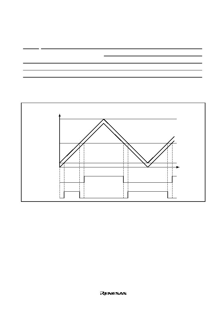
Rev. 2.0, 09/02, page 231 of 732
Table 11.27 Output Level Select Function
Bit 0
Function
Compare Match Output
OLSP
Initial Output
Active Level
Up Count
Down Count
0
High level
Low level
Low level
High level
1
Low level
High level
High level
Low level
Figure 11.2 shows an example of complementary PWM mode output (1 phase) when OLSN = 1,
OLSP = 1.
TCNT_3, and
TCNT_4 values
TGRA_3
TGRA_4
TDDR
H'0000
Time
TCNT_4
TCNT_3
Positive
phase output
Reverse
phase output
Active level
Compare match
output (up count)
Initial
output
Initial
output
Active
level
Compare match
output (down count)
Compare match
output (down count)
Compare match
output (up count)
Active level
Figure 11.2 Complementary PWM Mode Output Level Example
11.3.12
Timer Gate Control Register (TGCR)
TGCR is an 8-bit readable/writable register that controls the waveform output necessary for
brushless DC motor control in reset-synchronized PWM mode/complementary PWM mode.
These register settings are ineffective for anything other than complementary PWM mode/reset-
synchronized PWM mode.

Rev. 2.0, 09/02, page 232 of 732
Bit
Bit Name
Initial value
R/W
Description
7
--
1
R
Reserved
This bit is always read as 1 and should be written with
1.
6
BDC
0
R/W
Brushless DC Motor
This bit selects whether to make the functions of this
register (TGCR) effective or ineffective.
0: Ordinary output
1: Functions of this register are made effective
5
N
0
R/W
Reverse Phase Output (N) Control
This bit selects whether the level output or the reset-
synchronized PWM/complementary PWM output
while the reverse pins (TIOC3D, TIOC4C, and
TIOC4D) are output.
0: Level output
1: Reset synchronized PWM/complementary PWM
output
4
P
0
R/W
Positive Phase Output (P) Control
This bit selects whether the level output or the reset-
synchronized PWM/complementary PWM output
while the positive pin (TIOC3B, TIOC4A, and
TIOC4B) are output.
0: Level output
1: Reset synchronized PWM/complementary PWM
output
3
FB
0
R/W
External Feedback Signal Enable
This bit selects whether the switching of the output of
the positive/reverse phase is carried out automatically
with the MTU/channel 0 TGRA, TGRB, TGRC input
capture signals or by writing 0 or 1 to bits 2 to 0 in
TGCR.
0: Output switching is external input (Input sources
are channel 0 TGRA, TGRB, TGRC input capture
signal)
1: Output switching is carried out by software
(TGCR's UF, VF, WF settings).
2
1
0
WF
VF
UF
0
0
0
R/W
R/W
R/W
Output Phase Switch 2 to 0
These bits set the positive phase/negative phase
output phase on or off state. The setting of these bits
is valid only when the FB bit in this register is set to 1.
In this case, the setting of bits 2 to 0 is a substitute for
external input. See table 11.28.

Rev. 2.0, 09/02, page 233 of 732
Table 11.28 Output level Select Function
Function
Bit 2
Bit 1
Bit 0
TIOC3B
TIOC4A
TIOC4B
TIOC3D
TIOC4C
TIOC4D
WF
VF
UF
U Phase
V Phase
W Phase
U Phase
V Phase
W Phase
0
0
0
OFF
OFF
OFF
OFF
OFF
OFF
1
ON
OFF
OFF
OFF
OFF
ON
1
0
OFF
ON
OFF
ON
OFF
OFF
1
OFF
ON
OFF
OFF
OFF
ON
1
0
0
OFF
OFF
ON
OFF
ON
OFF
1
ON
OFF
OFF
OFF
ON
OFF
1
0
OFF
OFF
ON
ON
OFF
OFF
1
OFF
OFF
OFF
OFF
OFF
OFF
11.3.13
Timer Subcounter (TCNTS)
TCNTS is a 16-bit read-only counter that is used only in complementary PWM mode.
The initial value of TCNTS is H
0000.
Note:
Accessing the TCNTS in 8-bit units is prohibited. Always access in 16-bit units.
11.3.14
Timer Dead Time Data Register (TDDR)
TDDR is a 16-bit register, used only in complementary PWM mode, that specifies the TCNT_3
and TCNT_4 counter offset values. In complementary PWM mode, when the TCNT_3 and
TCNT_4 counters are cleared and then restarted, the TDDR register value is loaded into the
TCNT_3 counter and the count operation starts.
The initial value of TDDR is H
FFFF.
Note:
Accessing the TDDR in 8-bit units is prohibited. Always access in 16-bit units.

Rev. 2.0, 09/02, page 234 of 732
11.3.15
Timer Period Data Register (TCDR)
TCDR is a 16-bit register used only in complementary PWM mode. Set half the PWM carrier
sync value as the TCDR register value. This register is constantly compared with the TCNTS
counter in complementary PWM mode, and when a match occurs, the TCNTS counter switches
direction (decrement to increment).
The initial value of TCDR is H
FFFF.
Note:
Accessing the TCDR in 8-bit units is prohibited. Always access in 16-bit units.
11.3.16
Timer Period Buffer Register (TCBR)
The timer period buffer register (TCBR) is a 16-bit register used only in complementary PWM
mode. It functions as a buffer register for the TCDR register. The TCBR register values are
transferred to the TCDR register with the transfer timing set in the TMDR register.
Note:
Accessing the TCBR in 8-bit units is prohibited. Always access in 16-bit units.
11.3.17
Bus Master Interface
The timer counters (TCNT), general registers (TGR), timer subcounter (TCNTS), timer period
buffer register (TCBR), and timer dead time data register (TDDR), and timer period data register
(TCDR) are 16-bit registers. A 16-bit data bus to the bus master enables 16-bit read/writes. 8-bit
read/write is not possible. Always access in 16-bit units.
All registers other than the above registers are 8-bit registers. These are connected to the CPU by
a 16-bit data bus, so 16-bit read/writes and 8-bit read/writes are both possible.
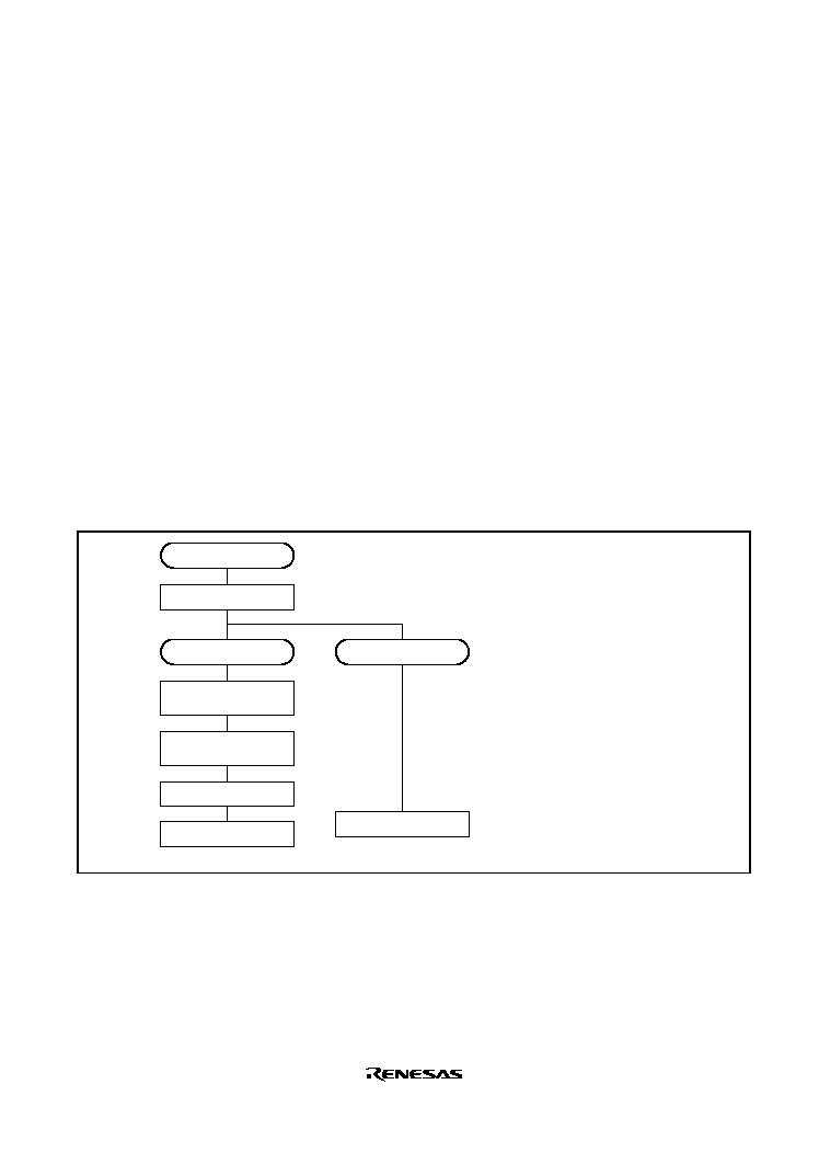
Rev. 2.0, 09/02, page 235 of 732
11.4
Operation
11.4.1
Basic Functions
Each channel has a TCNT and TGR register. TCNT performs up-counting, and is also capable of
free-running operation, synchronous counting, and external event counting.
Each TGR can be used as an input capture register or output compare register.
Always select MTU external pins set function using the pin function controller (PFC).
Counter Operation
When one of bits CST0 to CST4 is set to 1 in TSTR, the TCNT counter for the corresponding
channel begins counting. TCNT can operate as a free-running counter, periodic counter, for
example.
Example of Count Operation Setting Procedure: Figure 11.3 shows an example of the count
operation setting procedure.
Operation selection
Select counter clock
Periodic counter
Select counter clearing
source
Select output compare
register
Set period
Free-running counter
Start count operation
<Free-running counter>
<Periodic counter>
Start count operation
[1]
[2]
[3]
[4]
[5]
[5]
[1] Select the counter clock
with bits TPSC2 to TPSC0
in TCR. At the same time,
select the input clock edge
with bits CKEG1 and
CKEG0 in TCR.
[2] For periodic counter
operation, select the TGR
to be used as the TCNT
clearing source with bits
CCLR2 to CCLR0 in TCR.
[3] Designate the TGR
selected in [2] as an output
compare register by means
of TIOR.
[4] Set the periodic counter
cycle in the TGR selected
in [2].
[5] Set the CST bit in TSTR to
1 to start the counter
operation.
Figure 11.3 Example of Counter Operation Setting Procedure
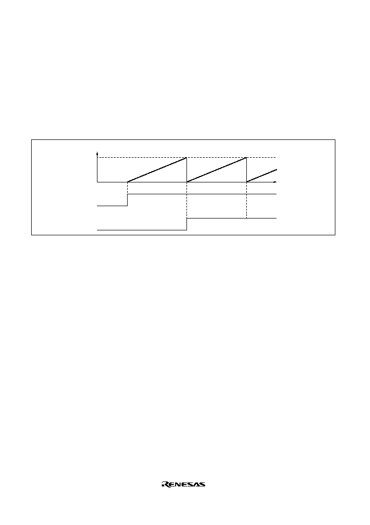
Rev. 2.0, 09/02, page 236 of 732
Free-Running Count Operation and Periodic Count Operation: Immediately after a reset, the
MTU's TCNT counters are all designated as free-running counters. When the relevant bit in TSTR
is set to 1 the corresponding TCNT counter starts up-count operation as a free-running counter.
When TCNT overflows (from H'FFFF to H'0000), the TCFV bit in TSR is set to 1. If the value of
the corresponding TCIEV bit in TIER is 1 at this point, the TPU requests an interrupt. After
overflow, TCNT starts counting up again from H'0000.
Figure 11.4 illustrates free-running counter operation.
TCNT value
H'FFFF
H'0000
CST bit
TCFV
Time
Figure 11.4 Free-Running Counter Operation
When compare match is selected as the TCNT clearing source, the TCNT counter for the relevant
channel performs periodic count operation. The TGR register for setting the period is designated
as an output compare register, and counter clearing by compare match is selected by means of bits
CCLR0 to CCLR2 in TCR. After the settings have been made, TCNT starts up-count operation as
a periodic counter when the corresponding bit in TSTR is set to 1. When the count value matches
the value in TGR, the TGF bit in TSR is set to 1 and TCNT is cleared to H'0000.
If the value of the corresponding TGIE bit in TIER is 1 at this point, the TPU requests an interrupt.
After a compare match, TCNT starts counting up again from H'0000.
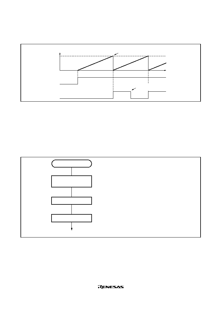
Rev. 2.0, 09/02, page 237 of 732
Figure 11.5 illustrates periodic counter operation.
TCNT value
TGR
H'0000
CST bit
TGF
Time
Counter cleared by TGR
compare match
Flag cleared by software or
DTC/DMAC activation
Figure 11.5 Periodic Counter Operation
Waveform Output by Compare Match
The MTU can perform 0, 1, or toggle output from the corresponding output pin using compare
match.
Example of Setting Procedure for Waveform Output by Compare Match: Figure 11.6 shows
an example of the setting procedure for waveform output by compare match
Output selection
Select waveform output
mode
Set output timing
Start count operation
<Waveform output>
[1]
[2]
[3]
[1] Select initial value 0 output or 1 output,
and compare match output value 0
output, 1 output, or toggle output, by
means of TIOR. The set initial value is
output at the TIOC pin until the first
compare match occurs.
[2] Set the timing for compare match
generation in TGR.
[3] Set the CST bit in TSTR to 1 to start the
count operation.
Figure 11.6 Example of Setting Procedure for Waveform Output by Compare Match
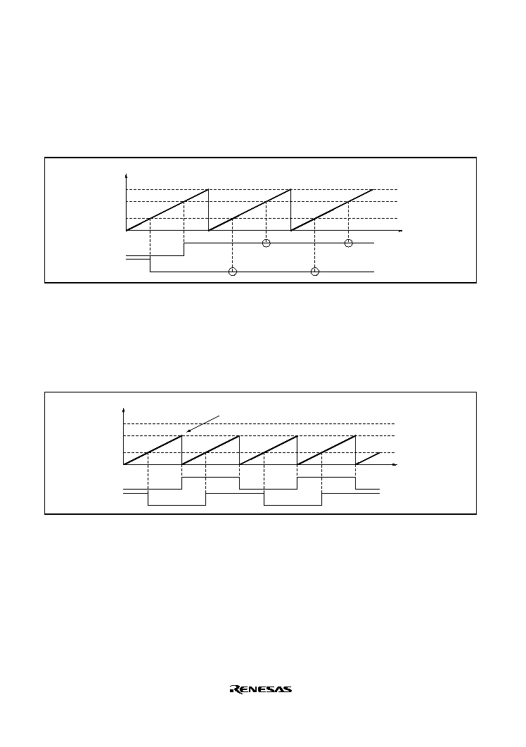
Rev. 2.0, 09/02, page 238 of 732
Examples of Waveform Output Operation: Figure 11.7 shows an example of 0 output/1 output.
In this example TCNT has been designated as a free-running counter, and settings have been made
such that 1 is output by compare match A, and 0 is output by compare match B. When the set level
and the pin level coincide, the pin level does not change.
TCNT value
H'FFFF
H'0000
TIOCA
TIOCB
Time
TGRA
TGRB
No change
No change
No change
No change
1 output
0 output
Figure 11.7 Example of 0 Output/1 Output Operation
Figure 11.8 shows an example of toggle output.
In this example, TCNT has been designated as a periodic counter (with counter clearing on
compare match B), and settings have been made such that the output is toggled by both compare
match A and compare match B.
TCNT value
H'FFFF
H'0000
TIOCB
TIOCA
Time
TGRB
TGRA
Toggle output
Toggle output
Counter cleared by TGRB compare match
Figure 11.8 Example of Toggle Output Operation
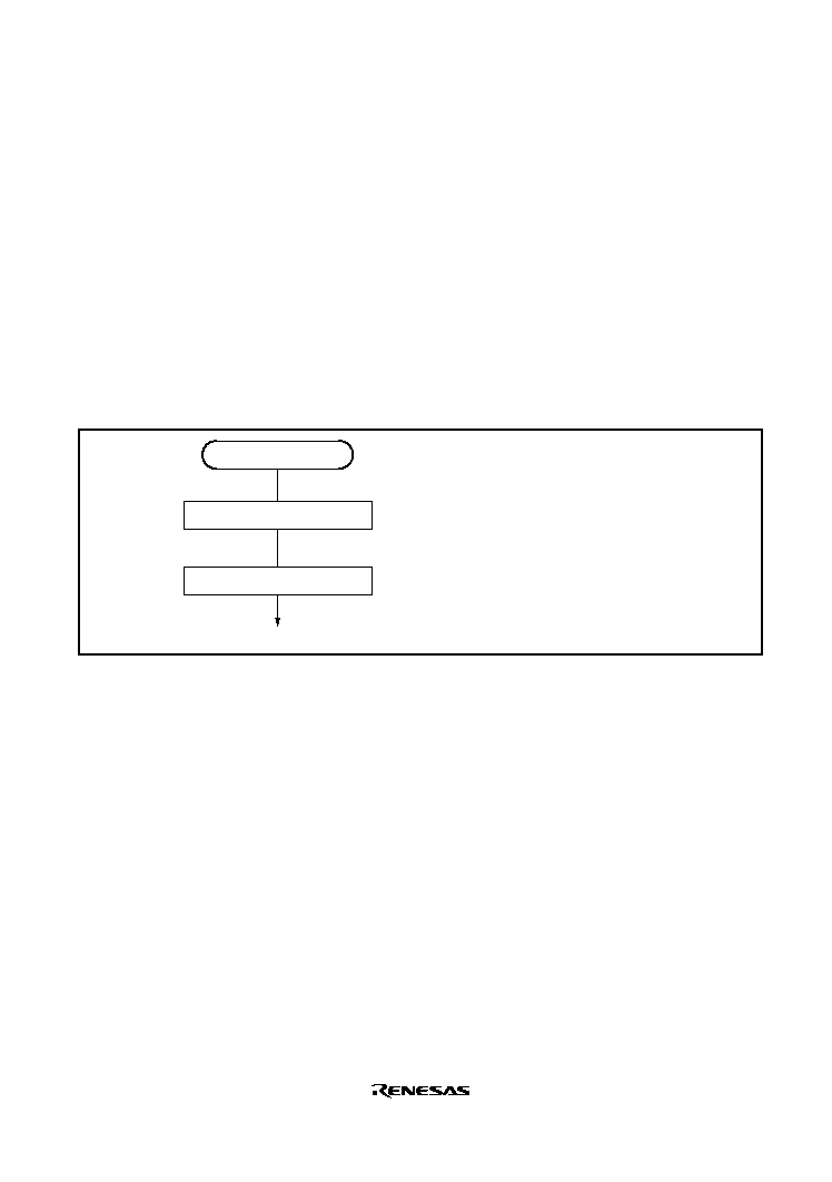
Rev. 2.0, 09/02, page 239 of 732
Input Capture Function
The TCNT value can be transferred to TGR on detection of the TIOC pin input edge.
Rising edge, falling edge, or both edges can be selected as the detected edge. For channels 0 and 1,
it is also possible to specify another channel's counter input clock or compare match signal as the
input capture source.
Note:
When another channel's counter input clock is used as the input capture input for channels
0 and 1, P
/1 should not be selected as the counter input clock used for input capture
input. Input capture will not be generated if P
/1 is selected.
Example of Input Capture Operation Setting Procedure: Figure 11.9 shows an example of the
input capture operation setting procedure.
Input selection
Select input capture input
Start count
<Input capture operation>
[1]
[2]
[1] Designate TGR as an input capture
register by means of TIOR, and select
rising edge, falling edge, or both edges
as the input capture source and input
signal edge.
[2] Set the CST bit in TSTR to 1 to start
the count operation.
Figure 11.9 Example of Input Capture Operation Setting Procedure
Example of Input Capture Operation: Figure 11.10 shows an example of input capture
operation.
In this example both rising and falling edges have been selected as the TIOCA pin input capture
input edge, the falling edge has been selected as the TIOCB pin input capture input edge, and
counter clearing by TGRB input capture has been designated for TCNT.
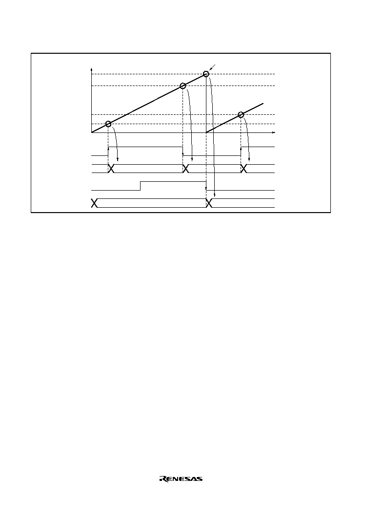
Rev. 2.0, 09/02, page 240 of 732
TCNT value
H'0180
H'0000
TIOCA
TGRA
H'0010
H'0005
Counter cleared by TIOCB
input (falling edge)
H'0160
H'0005
H'0160
H'0010
TGRB
H'0180
TIOCB
Time
Figure 11.10 Example of Input Capture Operation
11.4.2
Synchronous Operation
In synchronous operation, the values in a number of TCNT counters can be rewritten
simultaneously (synchronous presetting). Also, a number of TCNT counters can be cleared
simultaneously by making the appropriate setting in TCR (synchronous clearing).
Synchronous operation enables TGR to be incremented with respect to a single time base.
Channels 0 to 4 can all be designated for synchronous operation.

Rev. 2.0, 09/02, page 241 of 732
Example of Synchronous Operation Setting Procedure: Figure 11.11 shows an example of the
synchronous operation setting procedure.
No
Yes
Set synchronous
operation
<Synchronous presetting>
<Counter clearing>
<Synchronous clearing>
Clearing
source generation
channel?
Select counter
clearing source
Start count
Set synchronous
counter clearing
Start count
[1]
[3]
[5]
[4]
[5]
[2]
Synchronous operation
selection
[1] Set to 1 the SYNC bits in TSYR corresponding to the channels to be designated for synchronous
operation.
[2] When the TCNT counter of any of the channels designated for synchronous operation is written to,
the same value is simultaneously written to the other TCNT counters.
[3] Use bits CCLR2 to CCLR0 in TCR to specify TCNT clearing by input capture/output compare, etc.
[4] Use bits CCLR2 to CCLR0 in TCR to designate synchronous clearing for the counter clearing source.
[5] Set to 1 the CST bits in TSTR for the relevant channels, to start the count operation.
Set TCNT
Synchronous presetting
Synchronous clearing
Figure 11.11 Example of Synchronous Operation Setting Procedure
Example of Synchronous Operation: Figure 11.12 shows an example of synchronous operation.
In this example, synchronous operation and PWM mode 1 have been designated for channels 0 to
2, TGRB_0 compare match has been set as the channel 0 counter clearing source, and
synchronous clearing has been set for the channel 1 and 2 counter clearing source.
Three-phase PWM waveforms are output from pins TIOC0A, TIOC1A, and TIOC2A. At this
time, synchronous presetting, and synchronous clearing by TGRB_0 compare match, are
performed for channel 0 to 2 TCNT counters, and the data set in TGRB_0 is used as the PWM
cycle.
For details of PWM modes, see section 11.4.5, PWM Modes.
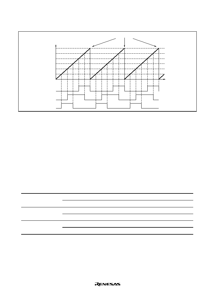
Rev. 2.0, 09/02, page 242 of 732
TCNT0 to TCNT2
values
H'0000
TIOC0A
TIOC1A
TGRB_0
Synchronous clearing by TGRB_0 compare match
TGRA_2
TGRA_1
TGRB_2
TGRA_0
TGRB_1
TIOC2A
Time
Figure 11.12 Example of Synchronous Operation
11.4.3
Buffer Operation
Buffer operation, provided for channels 0, 3, and 4, enables TGRC and TGRD to be used as buffer
registers.
Buffer operation differs depending on whether TGR has been designated as an input capture
register or as a compare match register.
Table 11.29 shows the register combinations used in buffer operation.
Table 11.29 Register Combinations in Buffer Operation
Channel
Timer General Register
Buffer Register
0
TGRA_0
TGRC_0
TGRB_0
TGRD_0
3
TGRA_3
TGRC_3
TGRB_3
TGRD_3
4
TGRA_4
TGRC_4
TGRB_4
TGRD_4
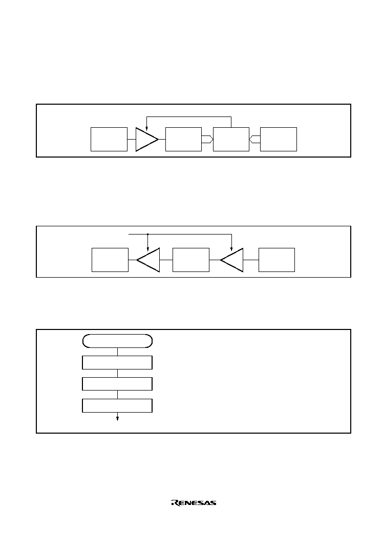
Rev. 2.0, 09/02, page 243 of 732
∑
When TGR is an output compare register
When a compare match occurs, the value in the buffer register for the corresponding channel is
transferred to the timer general register.
This operation is illustrated in figure 11.13.
Buffer
register
Timer general
register
TCNT
Comparator
Compare match signal
Figure 11.13 Compare Match Buffer Operation
∑
When TGR is an input capture register
When input capture occurs, the value in TCNT is transferred to TGR and the value previously
held in the timer general register is transferred to the buffer register.
This operation is illustrated in figure 11.14.
Buffer
register
Timer general
register
TCNT
Input capture
signal
Figure 11.14 Input Capture Buffer Operation
Example of Buffer Operation Setting Procedure: Figure 11.15 shows an example of the buffer
operation setting procedure.
Buffer operation
Select TGR function
Set buffer operation
Start count
<Buffer operation>
[1]
[2]
[3]
[1] Designate TGR as an input capture register or
output compare register by means of TIOR.
[2] Designate TGR for buffer operation with bits
BFA and BFB in TMDR.
[3] Set the CST bit in TSTR to 1 start the count
operation.
Figure 11.15 Example of Buffer Operation Setting Procedure
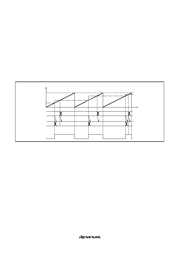
Rev. 2.0, 09/02, page 244 of 732
Examples of Buffer Operation:
∑
When TGR is an output compare register
Figure 11.16 shows an operation example in which PWM mode 1 has been designated for
channel 0, and buffer operation has been designated for TGRA and TGRC. The settings used
in this example are TCNT clearing by compare match B, 1 output at compare match A, and 0
output at compare match B.
As buffer operation has been set, when compare match A occurs the output changes and the
value in buffer register TGRC is simultaneously transferred to timer general register TGRA.
This operation is repeated each time that compare match A occurs.
For details of PWM modes, see section 11.4.5, PWM Modes.
TCNT value
TGRB_0
H'0000
TGRC_0
TGRA_0
H'0200
H'0520
TIOCA
H'0200
H'0450
H'0520
H'0450
TGRA_0
H'0450
H'0200
Transfer
Time
Figure 11.16 Example of Buffer Operation (1)
∑
When TGR is an input capture register
Figure 11.17 shows an operation example in which TGRA has been designated as an input
capture register, and buffer operation has been designated for TGRA and TGRC.
Counter clearing by TGRA input capture has been set for TCNT, and both rising and falling
edges have been selected as the TIOCA pin input capture input edge.
As buffer operation has been set, when the TCNT value is stored in TGRA upon the
occurrence of input capture A, the value previously stored in TGRA is simultaneously
transferred to TGRC.
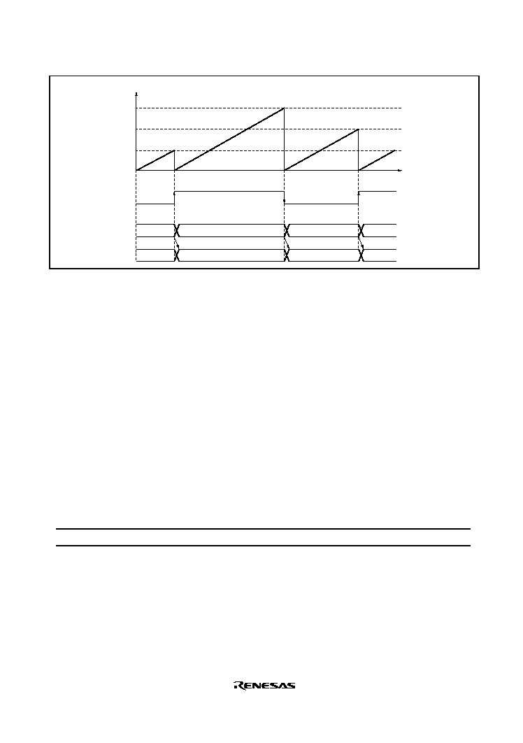
Rev. 2.0, 09/02, page 245 of 732
TCNT value
H'09FB
H'0000
TGRC
Time
H'0532
TIOCA
TGRA
H'0F07
H'0532
H'0F07
H'0532
H'0F07
H'09FB
Figure 11.17 Example of Buffer Operation (2)
11.4.4
Cascaded Operation
In cascaded operation, two 16-bit counters for different channels are used together as a 32-bit
counter.
This function works by counting the channel 1 counter clock upon overflow/underflow of
TCNT_2 as set in bits TPSC0 to TPSC2 in TCR.
Underflow occurs only when the lower 16-bit TCNT is in phase-counting mode.
Table 11.30 shows the register combinations used in cascaded operation.
Note: When phase counting mode is set for channel 1, the counter clock setting is invalid and the
counters operates independently in phase counting mode.
Table 11.30 Cascaded Combinations
Combination
Upper 16 Bits
Lower 16 Bits
Channels 1 and 2
TCNT_1
TCNT_2
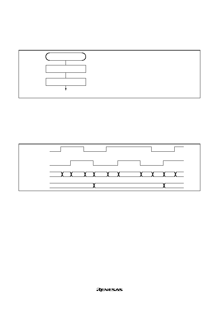
Rev. 2.0, 09/02, page 246 of 732
Example of Cascaded Operation Setting Procedure: Figure 11.18 shows an example of the
setting procedure for cascaded operation.
Cascaded operation
Set cascading
Start count
<Cascaded operation>
[1]
[2]
[1] Set bits TPSC2 to TPSC0 in the channel 1
TCR to B'1111 to select TCNT_2 overflow/
underflow counting.
[2] Set the CST bit in TSTR for the upper and
lower channel to 1 to start the count
operation.
Figure 11.18 Cascaded Operation Setting Procedure
Examples of Cascaded Operation: Figure 11.19 illustrates the operation when TCNT_2
overflow/underflow counting has been set for TCNT_1 and phase counting mode has been
designated for channel 2.
TCNT_1 is incremented by TCNT_2 overflow and decremented by TCNT_2 underflow.
TCLKC
TCNT_2
FFFD
TCNT_1
0001
TCLKD
FFFE
FFFF
0000
0001
0002
0001
0000
FFFF
0000
0000
Figure 11.19 Example of Cascaded Operation

Rev. 2.0, 09/02, page 247 of 732
11.4.5
PWM Modes
In PWM mode, PWM waveforms are output from the output pins. The output level can be selected
as 0, 1, or toggle output in response to a compare match of each TGR.
TGR registers settings can be used to output a PWM waveform in the range of 0% to 100% duty.
Designating TGR compare match as the counter clearing source enables the period to be set in that
register. All channels can be designated for PWM mode independently. Synchronous operation is
also possible.
There are two PWM modes, as described below.
∑
PWM mode 1
PWM output is generated from the TIOCA and TIOCC pins by pairing TGRA with TGRB and
TGRC with TGRD. The output specified by bits IOA0 to IOA3 and IOC0 to IOC3 in TIOR is
output from the TIOCA and TIOCC pins at compare matches A and C, and the output
specified by bits IOB0 to IOB3 and IOD0 to IOD3 in TIOR is output at compare matches B
and D. The initial output value is the value set in TGRA or TGRC. If the set values of paired
TGRs are identical, the output value does not change when a compare match occurs.
In PWM mode 1, a maximum 8-phase PWM output is possible.
∑
PWM mode 2
PWM output is generated using one TGR as the cycle register and the others as duty registers.
The output specified in TIOR is performed by means of compare matches. Upon counter
clearing by a synchronization register compare match, the output value of each pin is the initial
value set in TIOR. If the set values of the cycle and duty registers are identical, the output
value does not change when a compare match occurs.
In PWM mode 2, a maximum 8-phase PWM output is possible in combination use with
synchronous operation.
The correspondence between PWM output pins and registers is shown in table 11.31.

Rev. 2.0, 09/02, page 248 of 732
Table 11.31 PWM Output Registers and Output Pins
Output Pins
Channel
Registers
PWM Mode 1
PWM Mode 2
TGRA_0
TIOC0A
TGRB_0
TIOC0A
TIOC0B
TGRC_0
TIOC0C
0
TGRD_0
TIOC0C
TIOC0D
TGRA_1
TIOC1A
1
TGRB_1
TIOC1A
TIOC1B
TGRA_2
TIOC2A
2
TGRB_2
TIOC2A
TIOC2B
TGRA_3
Cannot be set
TGRB_3
TIOC3A
Cannot be set
TGRC_3
Cannot be set
3
TGRD_3
TIOC3C
Cannot be set
TGRA_4
Cannot be set
TGRB_4
TIOC4A
Cannot be set
TGRC_4
Cannot be set
4
TGRD_4
TIOC4C
Cannot be set
Note:
In PWM mode 2, PWM output is not possible for the TGR register in which the period is set.
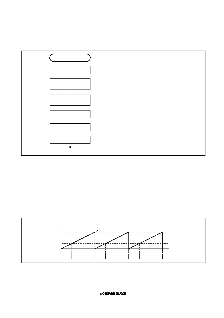
Rev. 2.0, 09/02, page 249 of 732
Example of PWM Mode Setting Procedure: Figure 11.20 shows an example of the PWM mode
setting procedure.
PWM mode
Select counter clock
Select counter clearing
source
Select waveform
output level
Set TGR
Set PWM mode
Start count
<PWM mode>
[1]
[2]
[3]
[4]
[5]
[6]
[1] Select the counter clock with bits TPSC2 to
TPSC0 in TCR. At the same time, select the
input clock edge with bits CKEG1 and
CKEG0 in TCR.
[2] Use bits CCLR2 to CCLR0 in TCR to select
the TGR to be used as the TCNT clearing
source.
[3] Use TIOR to designate the TGR as an output
compare register, and select the initial value
and output value.
[4] Set the cycle in the TGR selected in [2], and
set the duty in the other TGR.
[5] Select the PWM mode with bits MD3 to MD0
in TMDR.
[6] Set the CST bit in TSTR to 1 to start the
count operation.
Figure 11.20 Example of PWM Mode Setting Procedure
Examples of PWM Mode Operation: Figure 11.21 shows an example of PWM mode 1
operation.
In this example, TGRA compare match is set as the TCNT clearing source, 0 is set for the TGRA
initial output value and output value, and 1 is set as the TGRB output value.
In this case, the value set in TGRA is used as the period, and the values set in the TGRB registers
are used as the duty levels.
TCNT value
TGRA
H'0000
TIOCA
Time
TGRB
Counter cleared by
TGRA compare match
Figure 11.21 Example of PWM Mode Operation (1)
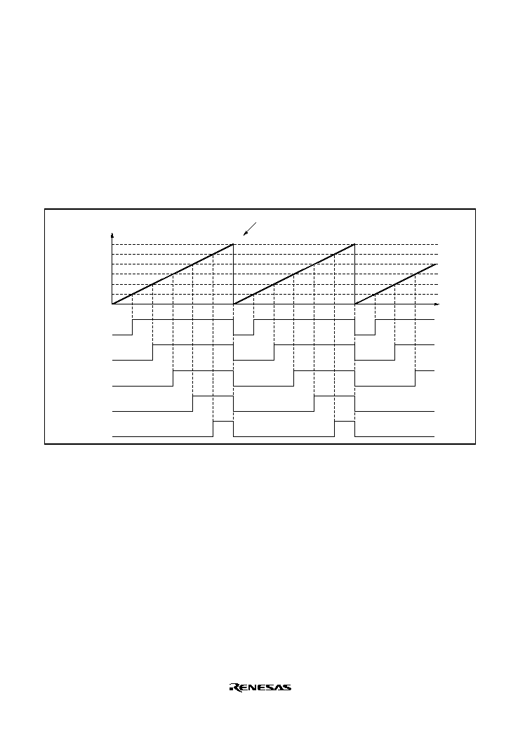
Rev. 2.0, 09/02, page 250 of 732
Figure 11.22 shows an example of PWM mode 2 operation.
In this example, synchronous operation is designated for channels 0 and 1, TGRB_1 compare
match is set as the TCNT clearing source, and 0 is set for the initial output value and 1 for the
output value of the other TGR registers (TGRA_0 to TGRD_0, TGRA_1), outputting a 5-phase
PWM waveform.
In this case, the value set in TGRB_1 is used as the cycle, and the values set in the other TGRs are
used as the duty levels.
TCNT value
TGRB_1
H'0000
TIOC0A
Counter cleared by
TGRB_1 compare match
Time
TGRA_1
TGRD_0
TGRC_0
TGRB_0
TGRA_0
TIOC0B
TIOC0C
TIOC0D
TIOC1A
Figure 11.22 Example of PWM Mode Operation (2)
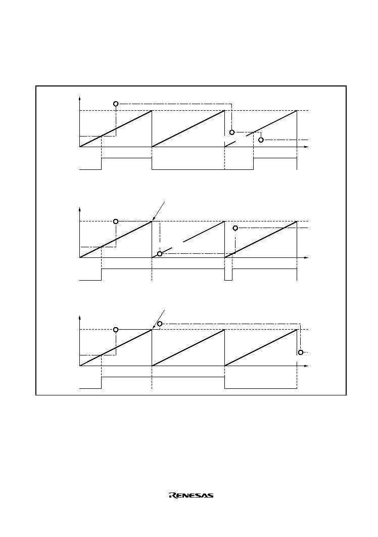
Rev. 2.0, 09/02, page 251 of 732
Figure 11.23 shows examples of PWM waveform output with 0% duty and 100% duty in PWM
mode.
TCNT value
TGRA
H'0000
TIOCA
Time
TGRB
0% duty
TGRB rewritten
TGRB
rewritten
TGRB rewritten
TCNT value
TGRA
H'0000
TIOCA
Time
TGRB
100% duty
TGRB rewritten
TGRB rewritten
TGRB rewritten
Output does not change when cycle register and duty register
compare matches occur simultaneously
TCNT value
TGRA
H'0000
TIOCA
Time
TGRB
100% duty
TGRB rewritten
TGRB rewritten
TGRB rewritten
Output does not change when cycle register and duty
register compare matches occur simultaneously
0% duty
Figure 11.23 Example of PWM Mode Operation (3)
Rev. 2.0, 09/02, page 252 of 732
11.4.6
Phase Counting Mode
In phase counting mode, the phase difference between two external clock inputs is detected and
TCNT is incremented/decremented accordingly. This mode can be set for channels 1 and 2.
When phase counting mode is set, an external clock is selected as the counter input clock and
TCNT operates as an up/down-counter regardless of the setting of bits TPSC0 to TPSC2 and bits
CKEG0 and CKEG1 in TCR. However, the functions of bits CCLR0 and CCLR1 in TCR, and of
TIOR, TIER, and TGR, are valid, and input capture/compare match and interrupt functions can be
used.
This can be used for two-phase encoder pulse input.
If overflow occurs when TCNT is counting up, the TCFV flag in TSR is set; if underflow occurs
when TCNT is counting down, the TCFU flag is set.
The TCFD bit in TSR is the count direction flag. Reading the TCFD flag reveals whether TCNT is
counting up or down.
Table 11.32 shows the correspondence between external clock pins and channels.
Table 11.32 Phase Counting Mode Clock Input Pins
External Clock Pins
Channels
A-Phase
B-Phase
When channel 1 is set to phase counting mode
TCLKA
TCLKB
When channel 2 is set to phase counting mode
TCLKC
TCLKD
Example of Phase Counting Mode Setting Procedure: Figure 11.24 shows an example of the
phase counting mode setting procedure.
Phase counting mode
Select phase counting
mode
Start count
<Phase counting mode>
[1]
[2]
[1] Select phase counting mode with bits
MD3 to MD0 in TMDR.
[2] Set the CST bit in TSTR to 1 to start
the count operation.
Figure 11.24 Example of Phase Counting Mode Setting Procedure
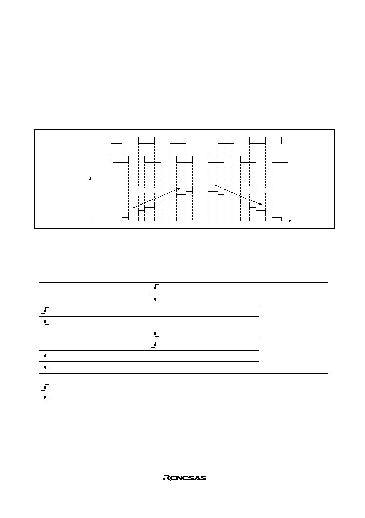
Rev. 2.0, 09/02, page 253 of 732
Examples of Phase Counting Mode Operation: In phase counting mode, TCNT counts up or
down according to the phase difference between two external clocks. There are four modes,
according to the count conditions.
∑
Phase counting mode 1
Figure 11.25 shows an example of phase counting mode 1 operation, and table 11.33
summarizes the TCNT up/down-count conditions.
TCNT value
Time
TCLKA (channel 1)
TCLKC (channel 2)
TCLKB (channel 1)
TCLKD (channel 2)
Up-count
Down-count
Figure 11.25 Example of Phase Counting Mode 1 Operation
Table 11.33 Up/Down-Count Conditions in Phase Counting Mode 1
TCLKA (Channel 1)
TCLKC (Channel 2)
TCLKB (Channel 1)
TCLKD (Channel 2)
Operation
High level
Up-count
Low level
Low level
High level
High level
Down-count
Low level
High level
Low level
Legend:
: Rising edge
: Falling edge
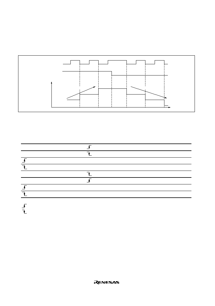
Rev. 2.0, 09/02, page 254 of 732
∑
Phase counting mode 2
Figure 11.26 shows an example of phase counting mode 2 operation, and table 11.34
summarizes the TCNT up/down-count conditions.
Time
Down-count
Up-count
TCNT value
TCLKA (channel 1)
TCLKC (channel 2)
TCLKB (channel 1)
TCLKD (channel 2)
Figure 11.26 Example of Phase Counting Mode 2 Operation
Table 11.34 Up/Down-Count Conditions in Phase Counting Mode 2
TCLKA (Channel 1)
TCLKC (Channel 2)
TCLKB (Channel 1)
TCLKD (Channel 2)
Operation
High level
Don't care
Low level
Don't care
Low level
Don't care
High level
Up-count
High level
Don't care
Low level
Don't care
High level
Don't care
Low level
Down-count
Legend:
: Rising edge
: Falling edge
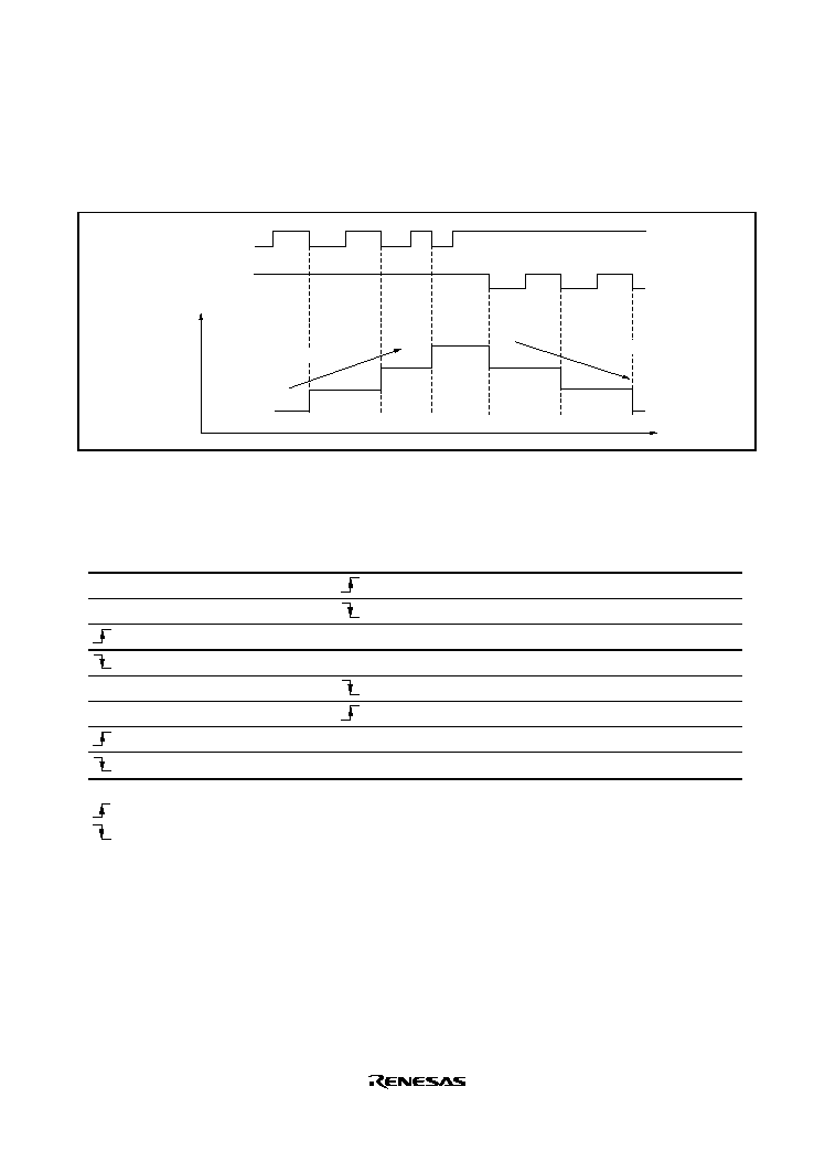
Rev. 2.0, 09/02, page 255 of 732
∑
Phase counting mode 3
Figure 11.27 shows an example of phase counting mode 3 operation, and table 11.35
summarizes the TCNT up/down-count conditions.
Time
Up-count
Down-count
TCNT value
TCLKA (channel 1)
TCLKC (channel 2)
TCLKB (channel 1)
TCLKD (channel 2)
Figure 11.27 Example of Phase Counting Mode 3 Operation
Table 11.35 Up/Down-Count Conditions in Phase Counting Mode 3
TCLKA (Channel 1)
TCLKC (Channel 2)
TCLKB (Channel 1)
TCLKD (Channel 2)
Operation
High level
Don't care
Low level
Don't care
Low level
Don't care
High level
Up-count
High level
Down-count
Low level
Don't care
High level
Don't care
Low level
Don't care
Legend:
: Rising edge
: Falling edge
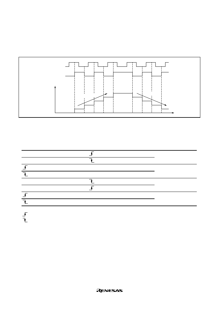
Rev. 2.0, 09/02, page 256 of 732
∑
Phase counting mode 4
Figure 11.28 shows an example of phase counting mode 4 operation, and table 11.36
summarizes the TCNT up/down-count conditions.
Time
Up-count
Down-count
TCNT value
TCLKA (channel 1)
TCLKC (channel 2)
TCLKB (channel 1)
TCLKD (channel 2)
Figure 11.28 Example of Phase Counting Mode 4 Operation
Table 11.36 Up/Down-Count Conditions in Phase Counting Mode 4
TCLKA (Channel 1)
TCLKC (Channel 2)
TCLKB (Channel 1)
TCLKD (Channel 2)
Operation
High level
Up-count
Low level
Low level
Don't care
High level
High level
Down-count
Low level
High level
Don't care
Low level
Legend:
: Rising edge
: Falling edge
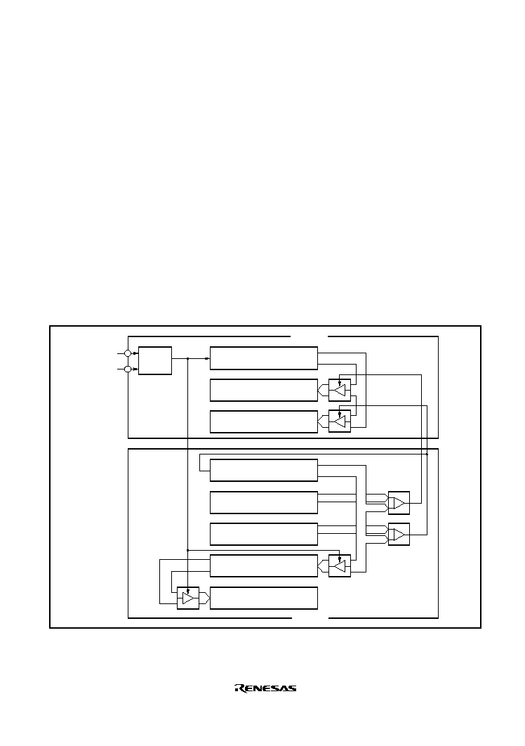
Rev. 2.0, 09/02, page 257 of 732
Phase Counting Mode Application Example: Figure 11.29 shows an example in which channel
1 is in phase counting mode, and channel 1 is coupled with channel 0 to input servo motor 2-phase
encoder pulses in order to detect position or speed.
Channel 1 is set to phase counting mode 1, and the encoder pulse A-phase and B-phase are input
to TCLKA and TCLKB.
Channel 0 operates with TCNT counter clearing by TGRC_0 compare match; TGRA_0 and
TGRC_0 are used for the compare match function and are set with the speed control period and
position control period. TGRB_0 is used for input capture, with TGRB_0 and TGRD_0 operating
in buffer mode. The channel 1 counter input clock is designated as the TGRB_0 input capture
source, and the pulse widths of 2-phase encoder 4-multiplication pulses are detected.
TGRA_1 and TGRB_1 for channel 1 are designated for input capture, and channel 0 TGRA_0 and
TGRC_0 compare matches are selected as the input capture source and store the up/down-counter
values for the control periods.
This procedure enables the accurate detection of position and speed.
TCNT_1
TCNT_0
Channel 1
TGRA_1
(speed period capture)
TGRA_0
(speed control period)
TGRB_1
(position period capture)
TGRC_0
(position control period)
TGRB_0 (pulse width capture)
TGRD_0 (buffer operation)
Channel 0
TCLKA
TCLKB
Edge
detection
circuit
+
-
+
-
Figure 11.29 Phase Counting Mode Application Example

Rev. 2.0, 09/02, page 258 of 732
11.4.7
Reset-Synchronized PWM Mode
In the reset-synchronized PWM mode, three-phase output of positive and negative PWM
waveforms that share a common wave transition point can be obtained by combining channels 3
and 4.
When set for reset-synchronized PWM mode, the TIOC3B, TIOC3D, TIOC4A, TIOC4C,
TIOC4B, and TIOC4D pins function as PWM output pins and TCNT3 functions as an upcounter.
Table 11.37 shows the PWM output pins used. Table 11.38 shows the settings of the registers.
Table 11.37 Output Pins for Reset-Synchronized PWM Mode
Channel
Output Pin
Description
3
TIOC3B
PWM output pin 1
TIOC3D
PWM output pin 1' (negative-phase waveform of PWM output 1)
4
TIOC4A
PWM output pin 2
TIOC4C
PWM output pin 2' (negative-phase waveform of PWM output 2)
TIOC4B
PWM output pin 3
TIOC4D
PWM output pin 3' (negative-phase waveform of PWM output 3)
Table 11.38 Register Settings for Reset-Synchronized PWM Mode
Register
Description of Setting
TCNT_3
Initial setting of H'0000
TCNT_4
Initial setting of H'0000
TGRA_3
Set count cycle for TCNT_3
TGRB_3
Sets the turning point for PWM waveform output by the TIOC3B and TIOC3D pins
TGRA_4
Sets the turning point for PWM waveform output by the TIOC4A and TIOC4C pins
TGRB_4
Sets the turning point for PWM waveform output by the TIOC4B and TIOC4D pins
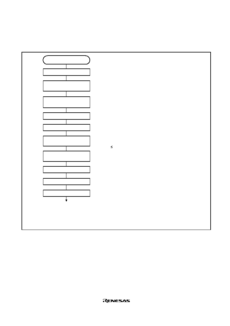
Rev. 2.0, 09/02, page 259 of 732
Procedure for Selecting the Reset-Synchronized PWM Mode: Figure 11.30 shows an example
of procedure for selecting the reset synchronized PWM mode.
Stop counting
Select counter clock and
counter clear source
Set TGR
Reset-synchronized
PWM mode
Brushless DC motor
control setting
Set TCNT
Enable waveform output
Set reset-synchronized
PWM mode
PWM cycle output enabling,
PWM output level setting
Start count operation
Reset-synchronized PWM mode
[1] Clear the CST3 and CST4 bits in the TSTR
to 0 to halt the counting of TCNT. The
reset-synchronized PWM mode must be set
up while TCNT_3 and TCNT_4 are halted.
[2] Set bits TPSC2-TPSC0 and CKEG1 and
CKEG0 in the TCR_3 to select the counter
clock and clock edge for channel 3. Set bits
CCLR2-CCLR0 in the TCR_3 to select TGRA
compare-match as a counter clear source.
[3] When performing brushless DC motor control,
set bit BDC in the timer gate control register
(TGCR) and set the feedback signal input source
and output chopping or gate signal direct output.
[4] Reset TCNT_3 and TCNT_4 to H'0000.
[5] TGRA_3 is the period register. Set the waveform
period value in TGRA_3. Set the transition timing
of the PWM output waveforms in TGRB_3,
TGRA_4, and TGRB_4. Set times within the
compare-match range of TCNT_3.
X TGRA_3 (X: set value).
[6] Select enabling/disabling of toggle output
synchronized with the PMW cycle using bit PSYE
in the timer output control register (TOCR), and set
the PWM output level with bits OLSP and OLSN.
[7] Set bits MD3-MD0 in TMDR_3 to B'1000 to select
the reset-synchronized PWM mode. Do not set to TMDR_4.
[8] Set the enabling/disabling of the PWM waveform output
pin in TOER.
[9] Set the port control register and the port I/O register.
[10] Set the CST3 bit in the TSTR to 1 to start the count
operation.
[1]
[2]
[3]
[4]
[5]
[6]
[7]
[8]
PFC setting
[9]
[10]
Note: The output waveform starts to toggle operation at the point of
TCNT_3 = TGRA_3 = X by setting X = TGRA, i.e., cycle = duty.
Figure 11.30 Procedure for Selecting the Reset-Synchronized PWM Mode
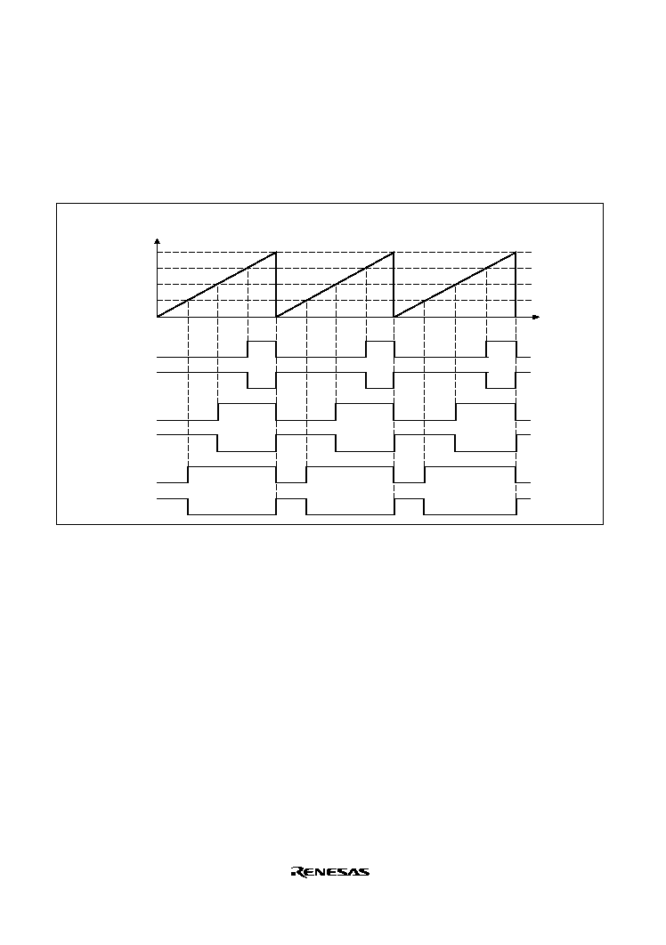
Rev. 2.0, 09/02, page 260 of 732
Reset-Synchronized PWM Mode Operation: Figure 11.31 shows an example of operation in the
reset-synchronized PWM mode. TCNT_3 and TCNT_4 operate as upcounters. The counter is
cleared when a TCNT_3 and TGRA_3 compare-match occurs, and then begins incrementing from
H'0000. The PWM output pin output toggles with each occurrence of a TGRB_3, TGRA_4,
TGRB_4 compare-match, and upon counter clears.
TGRA_3
TGRB_3
TGRB_4
H'0000
TGRA_4
TIOC3B
TIOC3D
TIOC4A
TIOC4C
TIOC4B
TIOC4D
Time
TCNT_3 and TCNT_4
values
Figure 11.31 Reset-Synchronized PWM Mode Operation Example
(When the TOCR's OLSN = 1 and OLSP = 1)

Rev. 2.0, 09/02, page 261 of 732
11.4.8
Complementary PWM Mode
In the complementary PWM mode, three-phase output of non-overlapping positive and negative
PWM waveforms can be obtained by combining channels 3 and 4.
In complementary PWM mode, TIOC3B, TIOC3D, TIOC4A, TIOC4B, TIOC4C, and TIOC4D
pins function as PWM output pins, the TIOC3A pin can be set for toggle output synchronized with
the PWM period. TCNT_3 and TCNT_4 function as up/down counters.
Table 11.39 shows the PWM output pins used. Table 11.40 shows the settings of the registers
used.
A function to directly cut off the PWM output by using an external signal is supported as a port
function.
Table 11.39 Output Pins for Complementary PWM Mode
Channel
Output Pin
Description
3
TIOC3A
Toggle output synchronized with PWM period (or I/O port)
TIOC3B
PWM output pin 1
TIOC3C
I/O port
*
TIOC3D
PWM output pin 1
(non-overlapping negative-phase waveform of PWM output 1)
4
TIOC4A
PWM output pin 2
TIOC4B
PWM output pin 3
TIOC4C
PWM output pin 2
(non-overlapping negative-phase waveform of PWM output 2)
TIOC4D
PWM output pin 3
(non-overlapping negative-phase waveform of PWM output 3)
Note:
*
Avoid setting the TIOC3C pin as a timer I/O pin in the complementary PWM mode.

Rev. 2.0, 09/02, page 262 of 732
Table 11.40 Register Settings for Complementary PWM Mode
Channel
Counter/Register
Description
Read/Write from CPU
3
TCNT_3
Start of up-count from value set
in dead time register
Maskable by BSC/BCR1
setting
*
TGRA_3
Set TCNT_3 upper limit value
(1/2 carrier cycle + dead time)
Maskable by BSC/BCR1
setting
*
TGRB_3
PWM output 1 compare register
Maskable by BSC/BCR1
setting
*
TGRC_3
TGRA_3 buffer register
Always readable/writable
TGRD_3
PWM output 1/TGRB_3 buffer
register
Always readable/writable
4
TCNT_4
Up-count start, initialized to
H'0000
Maskable by BSC/BCR1
setting
*
TGRA_4
PWM output 2 compare register
Maskable by BSC/BCR1
setting
*
TGRB_4
PWM output 3 compare register
Maskable by BSC/BCR1
setting
*
TGRC_4
PWM output 2/TGRA_4 buffer
register
Always readable/writable
TGRD_4
PWM output 3/TGRB_4 buffer
register
Always readable/writable
Timer dead time data register
(TDDR)
Set TCNT_4 and TCNT_3 offset
value (dead time value)
Maskable by BSC/BCR1
setting
*
Timer cycle data register
(TCDR)
Set TCNT_4 upper limit value
(1/2 carrier cycle)
Maskable by BSC/BCR1
setting
*
Timer cycle buffer register
(TCBR)
TCDR buffer register
Always readable/writable
Subcounter (TCNTS)
Subcounter for dead time
generation
Read-only
Temporary register 1 (TEMP1)
PWM output 1/TGRB_3
temporary register
Not readable/writable
Temporary register 2 (TEMP2)
PWM output 2/TGRA_4
temporary register
Not readable/writable
Temporary register 3 (TEMP3)
PWM output 3/TGRB_4
temporary register
Not readable/writable
Note:
*
Access can be enabled or disabled according to the setting of bit 13 (MTURWE) in
BSC/BCR1 (bus controller/bus control register 1).
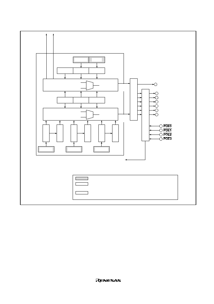
Rev. 2.0, 09/02, page 263 of 732
;
@
;
@
;
@
;
@
;
@
;
@
;
@
;
@
;
@
;
@
;
@
;
;;
@@
;;
@@
;;
@@
;;
@@
;;
@@
;;
@@
;;
@@
;;
@@
;;
@@
;;
@@
;;
@@
;;
;;
@@
;;
@@
;;
@@
;;
@@
;;
@@
;;
@@
;;
@@
;;
@@
;;
@@
;;
@@
;;
@@
;;
;;
;;
@@
@@
;;
;;
@@
@@
;;
;;
@@
@@
;;
;;
@@
@@
;;
;;
@@
@@
;;
;;
@@
@@
;;
;;
@@
@@
;;
;;
@@
@@
;;
;;
@@
@@
;;
;;
@@
@@
;;
;;
@@
@@
;;
;;
;;
;;
@@
@@
;;
;;
@@
@@
;;
;;
@@
@@
;;
;;
@@
@@
;;
;;
@@
@@
;;
;;
@@
@@
;;
;;
@@
@@
;;
;;
@@
@@
;;
;;
@@
@@
;;
;;
@@
@@
;;
;;
@@
@@
;;
;;
;
;
@
@
;
;
@
@
;
;
@
@
;
;
@
@
;
;
@
@
;
;
@
@
;
;
@
@
;
;
@
@
;
;
@
@
;
;
@
@
;
;
@
@
;
;
;;
;;
@@
@@
;;
;;
@@
@@
;;
;;
@@
@@
;;
;;
@@
@@
;;
;;
@@
@@
;;
;;
@@
@@
;;
;;
@@
@@
;;
;;
@@
@@
;;
;;
@@
@@
;;
;;
@@
@@
;;
;;
@@
@@
;;
;;
;;
;;
@@
@@
;;
;;
@@
@@
;;
;;
@@
@@
;;
;;
@@
@@
;;
;;
@@
@@
;;
;;
@@
@@
;;
;;
@@
@@
;;
;;
@@
@@
;;
;;
@@
@@
;;
;;
@@
@@
;;
;;
@@
@@
;;
;;
;
@
;
@
;
@
;
@
;
@
;
@
;
@
;
@
;
@
;
@
;
@
;
TGRC_3
TDDR
TCNT_3
TGRD_3
TGRD_4
TGRC_4
TGRB_3
Temp 1
TGRA_4
Temp 2
TGRB_4
Temp 3
TCNTS
TCNT_4
TGRA_3
TCDR
TCBR
Comparator
Comparator
Match
signal
Match
signal
Output controller
Output protection circuit
PWM cycle
output
PWM output 1
PWM output 2
PWM output 3
PWM output 4
PWM output 5
PWM output 6
External cutoff
input
External cutoff
interrupt
: Registers that can always be read or written from the CPU
: Registers that cannot be read or written from the CPU
(except for TCNTS, which can only be read)
: Registers that can be read or written from the CPU
(but for which access disabling can be set by the bus controller)
TGRA_3 compare-
match interrupt
TCNT_4 underflow
interrupt
Figure 11.32 Block Diagram of Channels 3 and 4 in Complementary PWM Mode

Rev. 2.0, 09/02, page 264 of 732
Example of Complementary PWM Mode Setting Procedure: An example of the
complementary PWM mode setting procedure is shown in figure 11.33.
Complementary PWM mode
Stop count operation
Counter clock, counter clear
source selection
Brushless DC motor control
setting
TCNT setting
Inter-channel synchronization
setting
TGR setting
Dead time, carrier cycle
setting
PWM cycle output enabling,
PWM output level setting
Complementary PWM mode
setting
Enable waveform output
Start count operation
<Complementary PWM mode>
[1] Clear bits CST3 and CST4 in the timer start register
(TSTR) to 0, and halt timer counter (TCNT) operation.
Perform complementary PWM mode setting when
TCNT_3 and TCNT_4 are stopped.
[2] Set the same counter clock and clock edge for channels
3 and 4 with bits TPSC2-TPSC0 and bits CKEG1 and
CKEG0 in the timer control register (TCR). Use bits
CCLR2-CCLR0 to set synchronous clearing only when
restarting by a synchronous clear from another channel
during complementary PWM mode operation.
[3] When performing brushless DC motor control, set bit BDC
in the timer gate control register (TGCR) and set the
feedback signal input source and output chopping or gate
signal direct output.
[4] Set the dead time in TCNT_3. Set TCNT_4 to H'0000.
[5] Set only when restarting by a synchronous clear from
another channel during complementary PWM mode
operation. In this case, synchronize the channel generating
the synchronous clear with channels 3 and 4 using the timer
synchro register (TSYR).
[6] Set the output PWM duty in the duty registers (TGRB_3,
TGRA_4, TGRB_4) and buffer registers (TGRD_3, TGRC_4,
TGRD_4). Set the same initial value in each corresponding
TGR.
[7] Set the dead time in the dead time register (TDDR), 1/2 the
carrier cycle in the carrier cycle data register (TCDR) and
carrier cycle buffer register (TCBR), and 1/2 the carrier cycle
plus the dead time in TGRA_3 and TGRC_3.
[8] Select enabling/disabling of toggle output synchronized with
the PWM cycle using bit PSYE in the timer output control
register (TOCR), and set the PWM output level with bits OLSP
and OLSN.
[9] Select complementary PWM mode in timer mode register 3
(TMDR_3). Do not set in TMDR_4.
[10] Set enabling/disabling of PWM waveform output pin output in
the timer output master enable register (TOER).
[11] Set the port control register and the port I/O register.
[12] Set bits CST3 and CST4 in TSTR to 1 simultaneously to start
the count operation.
[1]
[2]
[3]
[4]
[5]
[6]
[7]
[8]
[9]
[10]
PFC setting
[11]
[12]
Figure 11.33 Example of Complementary PWM Mode Setting Procedure

Rev. 2.0, 09/02, page 265 of 732
Outline of Complementary PWM Mode Operation
In complementary PWM mode, 6-phase PWM output is possible. Figure 11.34 illustrates counter
operation in complementary PWM mode, and figure 11.35 shows an example of complementary
PWM mode operation.
Counter Operation: In complementary PWM mode, three counters--TCNT_3, TCNT_4, and
TCNTS--perform up/down-count operations.
TCNT_3 is automatically initialized to the value set in TDDR when complementary PWM mode
is selected and the CST bit in TSTR is 0.
When the CST bit is set to 1, TCNT_3 counts up to the value set in TGRA_3, then switches to
down-counting when it matches TGRA_3,. When the TCNT3 value matches TDDR, the counter
switches to up-counting, and the operation is repeated in this way.
TCNT_4 is initialized to H'0000.
When the CST bit is set to 1, TCNT4 counts up in synchronization with TCNT_3, and switches to
down-counting when it matches TCDR . On reaching H'0000, TCNT4 switches to up-counting,
and the operation is repeated in this way.
TCNTS is a read-only counter. It need not be initialized.
When TCNT_3 matches TCDR during TCNT_3 and TCNT_4 up/down-counting, down-counting
is started, and when TCNTS matches TCDR, the operation switches to up-counting. When
TCNTS matches TGRA_3, it is cleared to H'0000.
When TCNT_4 matches TDDR during TCNT_3 and TCNT_4 down-counting, up-counting is
started, and when TCNTS matches TDDR, the operation switches to down-counting. When
TCNTS reaches H'0000, it is set with the value in TGRA_3.
TCNTS is compared with the compare register and temporary register in which the PWM duty is
set during the count operation only.
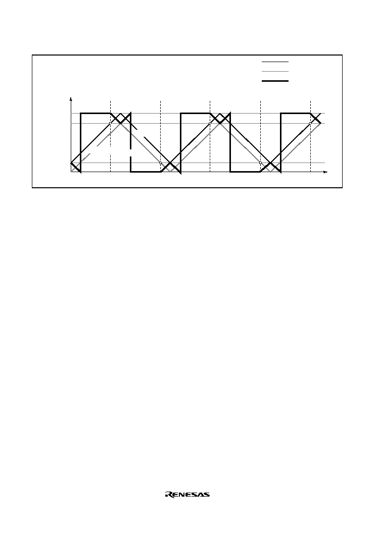
Rev. 2.0, 09/02, page 266 of 732
Counter value
TGRA_3
TCDR
TDDR
H'0000
TCNT_4
TCNTS
TCNT_3
TCNT_3
TCNT_4
TCNTS
Time
Figure 11.34 Complementary PWM Mode Counter Operation
Register Operation: In complementary PWM mode, nine registers are used, comprising compare
registers, buffer registers, and temporary registers. Figure 11.35 shows an example of
complementary PWM mode operation.
The registers which are constantly compared with the counters to perform PWM output are
TGRB_3, TGRA_4, and TGRB_4. When these registers match the counter, the value set in bits
OLSN and OLSP in the timer output control register (TOCR) is output.
The buffer registers for these compare registers are TGRD_3, TGRC_4, and TGRD_4.
Between a buffer register and compare register there is a temporary register. The temporary
registers cannot be accessed by the CPU.
Data in a compare register is changed by writing the new data to the corresponding buffer register.
The buffer registers can be read or written at any time.
The data written to a buffer register is constantly transferred to the temporary register in the Ta
interval. Data is not transferred to the temporary register in the Tb interval. Data written to a
buffer register in this interval is transferred to the temporary register at the end of the Tb interval.
The value transferred to a temporary register is transferred to the compare register when TCNTS
for which the Tb interval ends matches TGRA_3 when counting up, or H'0000 when counting
down. The timing for transfer from the temporary register to the compare register can be selected
with bits MD3 to MD0 in the timer mode register (TMDR). Figure 11.35 shows an example in
which the mode is selected in which the change is made in the trough.
In the tb interval (tb1 in figure 11.35) in which data transfer to the temporary register is not
performed, the temporary register has the same function as the compare register, and is compared
with the counter. In this interval, therefore, there are two compare match registers for one-phase
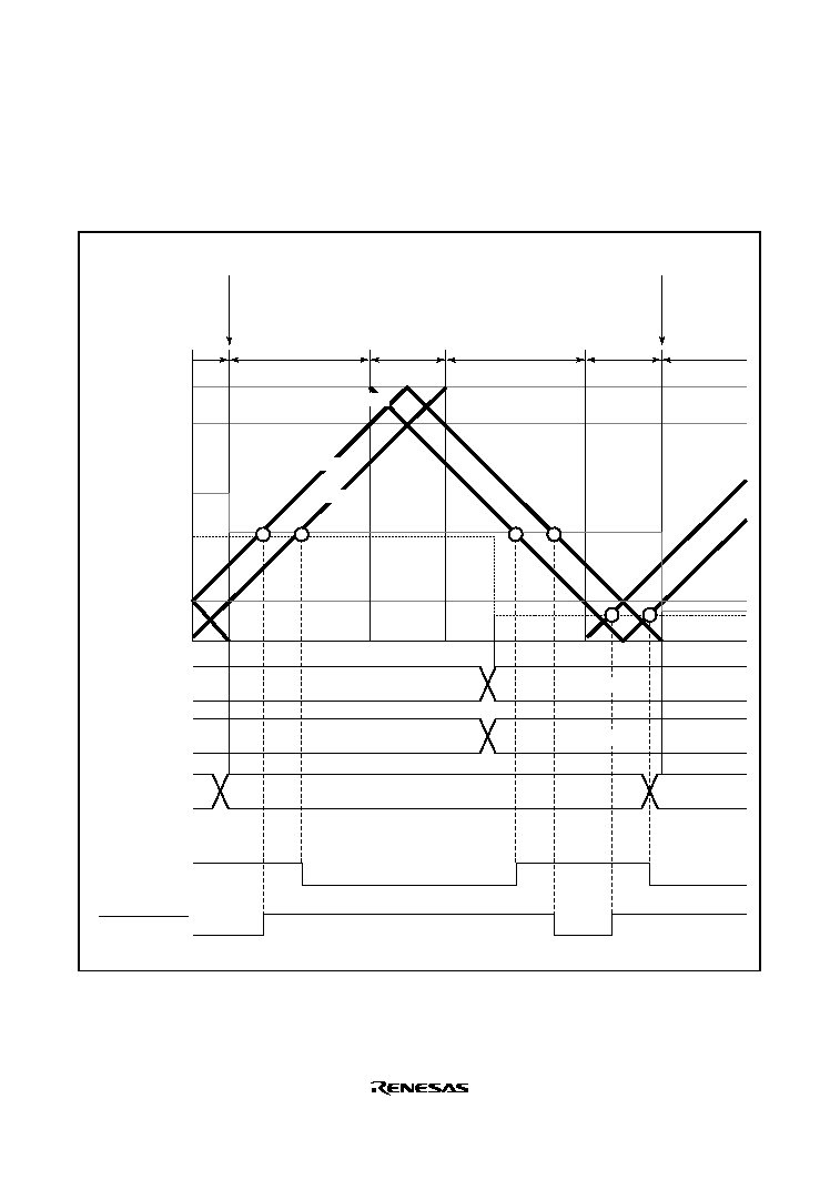
Rev. 2.0, 09/02, page 267 of 732
output, with the compare register containing the pre-change data, and the temporary register
containing the new data. In this interval, the three counters--TCNT_3, TCNT_4, and TCNTS--
and two registers--compare register and temporary register--are compared, and PWM output
controlled accordingly.
TGRA_3
TCDR
TGRA_4
TGRC_4
TDDR
H'0000
Buffer register
TGRC_4
Temporary register
TEMP2
Compare register
TGRA_4
Output waveform
Output waveform
Tb2
Ta
Tb1
Ta
Tb2
Ta
TCNT_3
TCNT_4
TCNTS
(Output waveform is active-low)
H'6400
H'0080
H'6400
H'6400
H'0080
H'0080
Transfer from temporary
register to compare register
Transfer from temporary
register to compare register
Figure 11.35 Example of Complementary PWM Mode Operation

Rev. 2.0, 09/02, page 268 of 732
Initialization: In complementary PWM mode, there are six registers that must be initialized.
Before setting complementary PWM mode with bits MD3 to MD0 in the timer mode register
(TMDR), the following initial register values must be set.
TGRC_3 operates as the buffer register for TGRA_3, and should be set with 1/2 the PWM carrier
cycle + dead time Td. The timer cycle buffer register (TCBR) operates as the buffer register for
the timer cycle data register (TCDR), and should be set with 1/2 the PWM carrier cycle. Set dead
time Td in the timer dead time data register (TDDR).
Set the respective initial PWM duty values in buffer registers TGRD_3, TGRC_4, and TGRD_4.
The values set in the five buffer registers excluding TDDR are transferred simultaneously to the
corresponding compare registers when complementary PWM mode is set.
Set TCNT_4 to H'0000 before setting complementary PWM mode.
Table 11.41 Registers and Counters Requiring Initialization
Register/Counter
Set Value
TGRC_3
1/2 PWM carrier cycle + dead time Td
TDDR
Dead time Td
TCBR
1/2 PWM carrier cycle
TGRD_3, TGRC_4, TGRD_4
Initial PWM duty value for each phase
TCNT_4
H'0000
Note:
The TGRC_3 set value must be the sum of 1/2 the PWM carrier cycle set in TCBR and
dead time Td set in TDDR.
PWM Output Level Setting: In complementary PWM mode, the PWM pulse output level is set
with bits OLSN and OLSP in the timer output control register (TOCR).
The output level can be set for each of the three positive phases and three negative phases of 6-
phase output.
Complementary PWM mode should be cleared before setting or changing output levels.
Dead Time Setting: In complementary PWM mode, PWM pulses are output with a non-
overlapping relationship between the positive and negative phases. This non-overlap time is called
the dead time.
The non-overlap time is set in the timer dead time data register (TDDR). The value set in TDDR is
used as the TCNT_3 counter start value, and creates non-overlap between TCNT_3 and TCNT_4.
Complementary PWM mode should be cleared before changing the contents of TDDR.
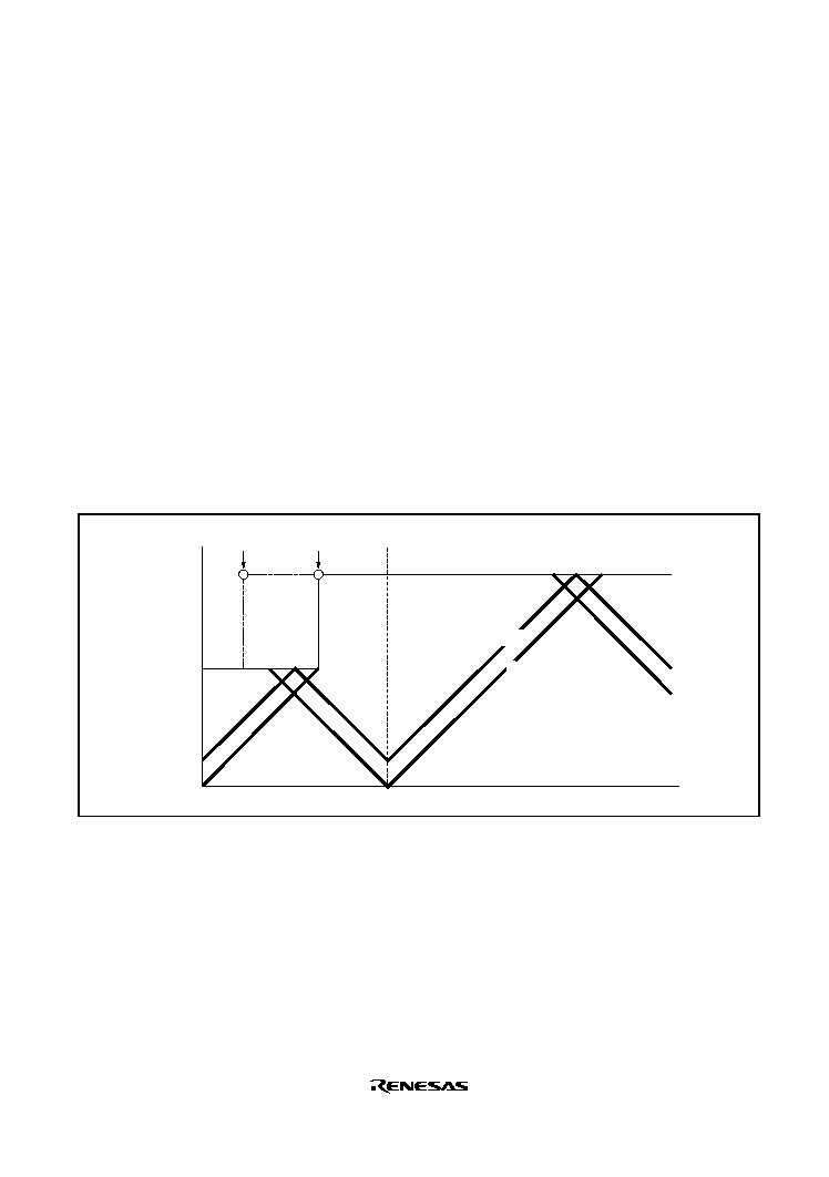
Rev. 2.0, 09/02, page 269 of 732
PWM Cycle Setting: In complementary PWM mode, the PWM pulse cycle is set in two
registers--TGRA_3, in which the TCNT_3 upper limit value is set, and TCDR, in which the
TCNT_4 upper limit value is set. The settings should be made so as to achieve the following
relationship between these two registers:
TGRA_3 set value = TCDR set value + TDDR set value
The TGRA_3 and TCDR settings are made by setting the values in buffer registers TGRC_3 and
TCBR. The values set in TGRC_3 and TCBR are transferred simultaneously to TGRA_3 and
TCDR in accordance with the transfer timing selected with bits MD3 to MD0 in the timer mode
register (TMDR).
The updated PWM cycle is reflected from the next cycle when the data update is performed at the
crest, and from the current cycle when performed in the trough. Figure 11.36 illustrates the
operation when the PWM cycle is updated at the crest.
See the following section, Register Data Updating, for the method of updating the data in each
buffer register.
Counter value
TGRC_3
update
TGRA_3
update
TGRA_3
TCNT_3
TCNT_4
Time
Figure 11.36 Example of PWM Cycle Updating

Rev. 2.0, 09/02, page 270 of 732
Register Data Updating: In complementary PWM mode, the buffer register is used to update the
data in a compare register. The update data can be written to the buffer register at any time. There
are five PWM duty and carrier cycle registers that have buffer registers and can be updated during
operation.
There is a temporary register between each of these registers and its buffer register. When
subcounter TCNTS is not counting, if buffer register data is updated, the temporary register value
is also rewritten. Transfer is not performed from buffer registers to temporary registers when
TCNTS is counting; in this case, the value written to a buffer register is transferred after TCNTS
halts.
The temporary register value is transferred to the compare register at the data update timing set
with bits MD3 to MD0 in the timer mode register (TMDR). Figure 11.37 shows an example of
data updating in complementary PWM mode. This example shows the mode in which data
updating is performed at both the counter crest and trough.
When rewriting buffer register data, a write to TGRD_4 must be performed at the end of the
update. Data transfer from the buffer registers to the temporary registers is performed
simultaneously for all five registers after the write to TGRD_4.
A write to TGRD_4 must be performed after writing data to the registers to be updated, even when
not updating all five registers, or when updating the TGRD_4 data. In this case, the data written to
TGRD_4 should be the same as the data prior to the write operation.
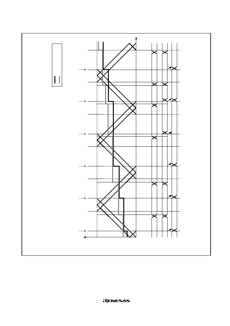
Rev. 2.0, 09/02, page 271 of 732
Data update timing: counter crest and trough
Transfer from
temporary register
to compare register
Transfer from
temporary register
to compare register
Transfer from
temporary register
to compare register
Transfer from
temporary register
to compare register
Transfer from
temporary register
to compare register
Transfer from
temporary register
to compare register
Counter value
TGRA_3
TGRC_4
TGRA_4
H'0000
BR
data1
data2
data3
data4
data5
data6
data1
data1
data2
data3
data4
data6
data2
data3
data4
data5
data6
Temp_R
GR
Time
: Compare register
: Buffer register
Figure 11.37 Example of Data Update in Complementary PWM Mode
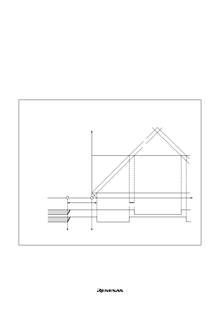
Rev. 2.0, 09/02, page 272 of 732
Initial Output in Complementary PWM Mode: In complementary PWM mode, the initial
output is determined by the setting of bits OLSN and OLSP in the timer output control register
(TOCR).
This initial output is the PWM pulse non-active level, and is output from when complementary
PWM mode is set with the timer mode register (TMDR) until TCNT_4 exceeds the value set in
the dead time register (TDDR). Figure 11.38 shows an example of the initial output in
complementary PWM mode.
An example of the waveform when the initial PWM duty value is smaller than the TDDR value is
shown in figure 11.39.
Timer output control register settings
OLSN bit: 0 (initial output: high; active level: low)
OLSP bit: 0 (initial output: high; active level: low)
TCNT3, 4 value
TGR4_A
TDDR
TCNT_3
TCNT_4
Initial output
Dead time
Time
Active level
Active level
TCNT3, 4 count start
(TSTR setting)
Complementary
PWM mode
(TMDR setting)
Positive phase
output
Negative phase
output
Figure 11.38 Example of Initial Output in Complementary PWM Mode (1)

Rev. 2.0, 09/02, page 273 of 732
Timer output control register settings
OLSN bit: 0 (initial output: high; active level: low)
OLSP bit: 0 (initial output: high; active level: low)
TCNT_3, 4 value
TGRA_4
TDDR
TCNT_3
TCNT_4
Initial output
Time
Active level
TCNT_3, 4 count start
(TSTR setting)
Complementary
PWM mode
(TMDR setting)
Positive phase
output
Negative phase
output
Figure 11.39 Example of Initial Output in Complementary PWM Mode (2)
Complementary PWM Mode PWM Output Generation Method: In complementary PWM
mode, 3-phase output is performed of PWM waveforms with a non-overlap time between the
positive and negative phases. This non-overlap time is called the dead time.
A PWM waveform is generated by output of the output level selected in the timer output control
register in the event of a compare-match between a counter and data register. While TCNTS is
counting, data register and temporary register values are simultaneously compared to create
consecutive PWM pulses from 0 to 100%. The relative timing of on and off compare-match
occurrence may vary, but the compare-match that turns off each phase takes precedence to secure
the dead time and ensure that the positive phase and negative phase on times do not overlap.
Figures 11.40 to 11.42 show examples of waveform generation in complementary PWM mode.
The positive phase/negative phase off timing is generated by a compare-match with the solid-line
counter, and the on timing by a compare-match with the dotted-line counter operating with a delay
of the dead time behind the solid-line counter. In the T1 period, compare-match a that turns off the
negative phase has the highest priority, and compare-matches occurring prior to a are ignored. In
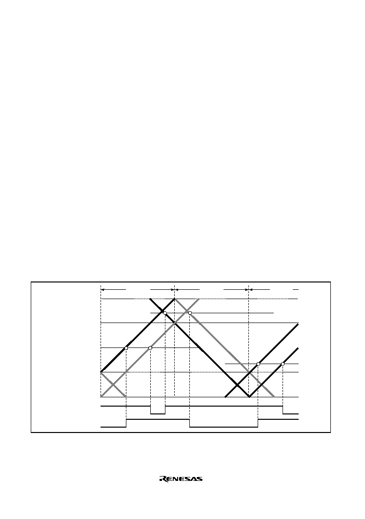
Rev. 2.0, 09/02, page 274 of 732
the T2 period, compare-match c that turns off the positive phase has the highest priority, and
compare-matches occurring prior to c are ignored.
In normal cases, compare-matches occur in the order a
b
c
d (or c
d
a'
b'), as
shown in figure 11.40.
If compare-matches deviate from the a
b
c
d order, since the time for which the negative
phase is off is less than twice the dead time, the figure shows the positive phase is not being turned
on. If compare-matches deviate from the c
d
a'
b' order, since the time for which the
positive phase is off is less than twice the dead time, the figure shows the negative phase is not
being turned on.
If compare-match c occurs first following compare-match a, as shown in figure 11.41, compare-
match b is ignored, and the negative phase is turned off by compare-match d. This is because
turning off of the positive phase has priority due to the occurrence of compare-match c (positive
phase off timing) before compare-match b (positive phase on timing) (consequently, the waveform
does not change since the positive phase goes from off to off).
Similarly, in the example in figure 11.42, compare-match a' with the new data in the temporary
register occurs before compare-match c, but other compare-matches occurring up to c, which turns
off the positive phase, are ignored. As a result, the positive phase is not turned on.
Thus, in complementary PWM mode, compare-matches at turn-off timings take precedence, and
turn-on timing compare-matches that occur before a turn-off timing compare-match are ignored.
T2 period
T1 period
T1 period
a
b
c
a'
b'
d
TGR3A_3
TCDR
TDDR
H'0000
Positive phase
Negative phase
Figure 11.40 Example of Complementary PWM Mode Waveform Output (1)
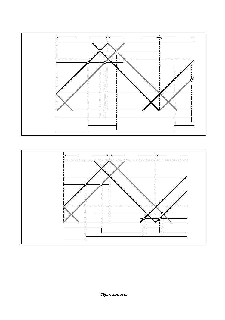
Rev. 2.0, 09/02, page 275 of 732
T2 period
T1 period
T1 period
TGRA_3
TCDR
TDDR
H'0000
Positive phase
Negative phase
c
d
a
a
b
b
Figure 11.41 Example of Complementary PWM Mode Waveform Output (2)
a
b
c
a'
b'
d
T1 period
T2 period
T1 period
TGRA_3
TCDR
TDDR
H'0000
Positive phase
Negative phase
Figure 11.42 Example of Complementary PWM Mode Waveform Output (3)
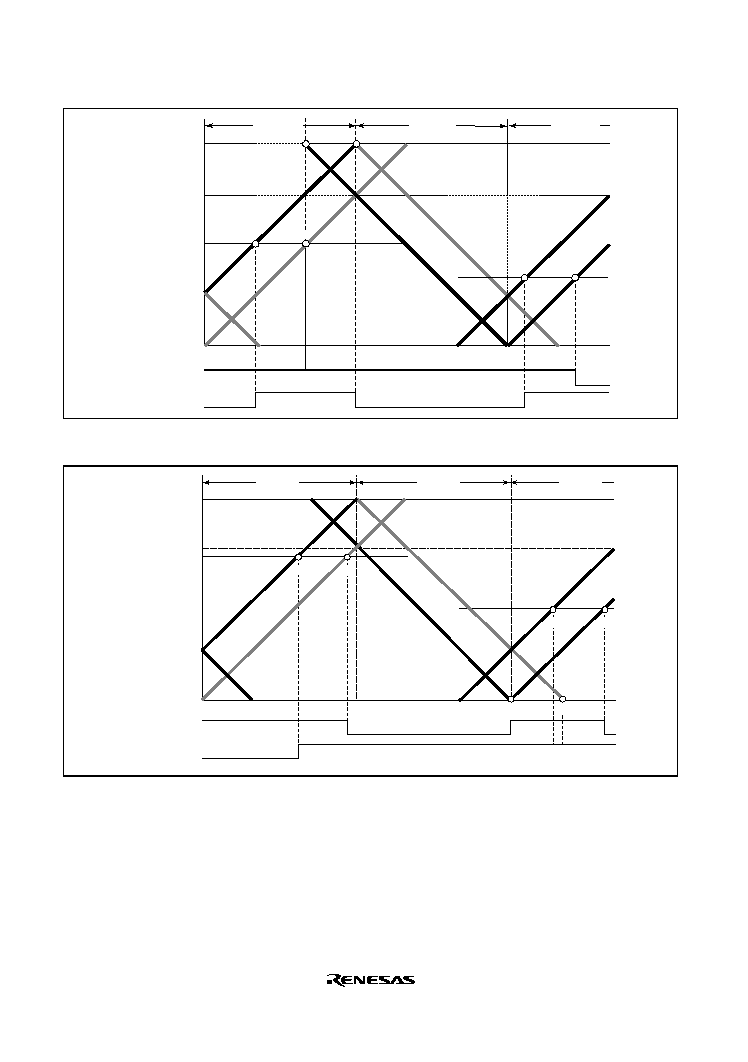
Rev. 2.0, 09/02, page 276 of 732
a
b
c
d
a'
b'
T2 period
T1 period
T1 period
TGRA_3
TCDR
TDDR
H'0000
Positive phase
Negative phase
Figure 11.43 Example of Complementary PWM Mode 0% and 100% Waveform Output (1)
T2 period
T1 period
T1 period
TGRA_3
TCDR
TDDR
H'0000
Positive phase
Negative phase
a
c
d
a
b
b
Figure 11.44 Example of Complementary PWM Mode 0% and 100% Waveform Output (2)
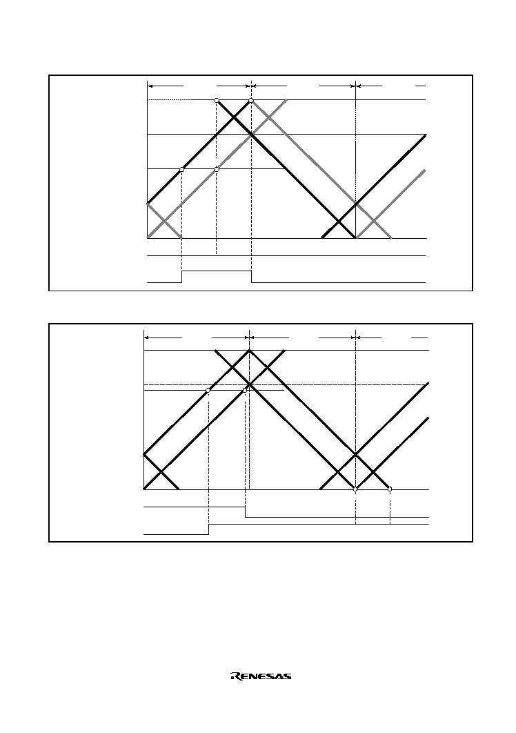
Rev. 2.0, 09/02, page 277 of 732
T2 period
T1 period
T1 period
a
b
c
d
TGRA_3
TCDR
TDDR
H'0000
Positive phase
Negative phase
Figure 11.45 Example of Complementary PWM Mode 0% and 100% Waveform Output (3)
TGRA_3
TCDR
TDDR
H'0000
Positive phase
Negative phase
T2 period
T1 period
T1 period
a
b
c b'
d a'
Figure 11.46 Example of Complementary PWM Mode 0% and 100% Waveform Output (4)

Rev. 2.0, 09/02, page 278 of 732
c
a d
b
T2 period
T1 period
T1 period
TGRA_3
TCDR
TDDR
H'0000
Positive phase
Negative phase
Figure 11.47 Example of Complementary PWM Mode 0% and 100% Waveform Output (5)
Complementary PWM Mode 0% and 100% Duty Output: In complementary PWM mode, 0%
and 100% duty cycles can be output as required. Figures 11.43 to 11.47 show output examples.
100% duty output is performed when the data register value is set to H'0000. The waveform in this
case has a positive phase with a 100% on-state. 0% duty output is performed when the data
register value is set to the same value as TGRA_3. The waveform in this case has a positive phase
with a 100% off-state.
On and off compare-matches occur simultaneously, but if a turn-on compare-match and turn-off
compare-match for the same phase occur simultaneously, both compare-matches are ignored and
the waveform does not change.
Toggle Output Synchronized with PWM Cycle: In complementary PWM mode, toggle output
can be performed in synchronization with the PWM carrier cycle by setting the PSYE bit to 1 in
the timer output control register (TOCR). An example of a toggle output waveform is shown in
figure 11.48.
This output is toggled by a compare-match between TCNT_3 and TGRA_3 and a compare-match
between TCNT4 and H'0000.
The output pin for this toggle output is the TIOC3A pin. The initial output is 1.
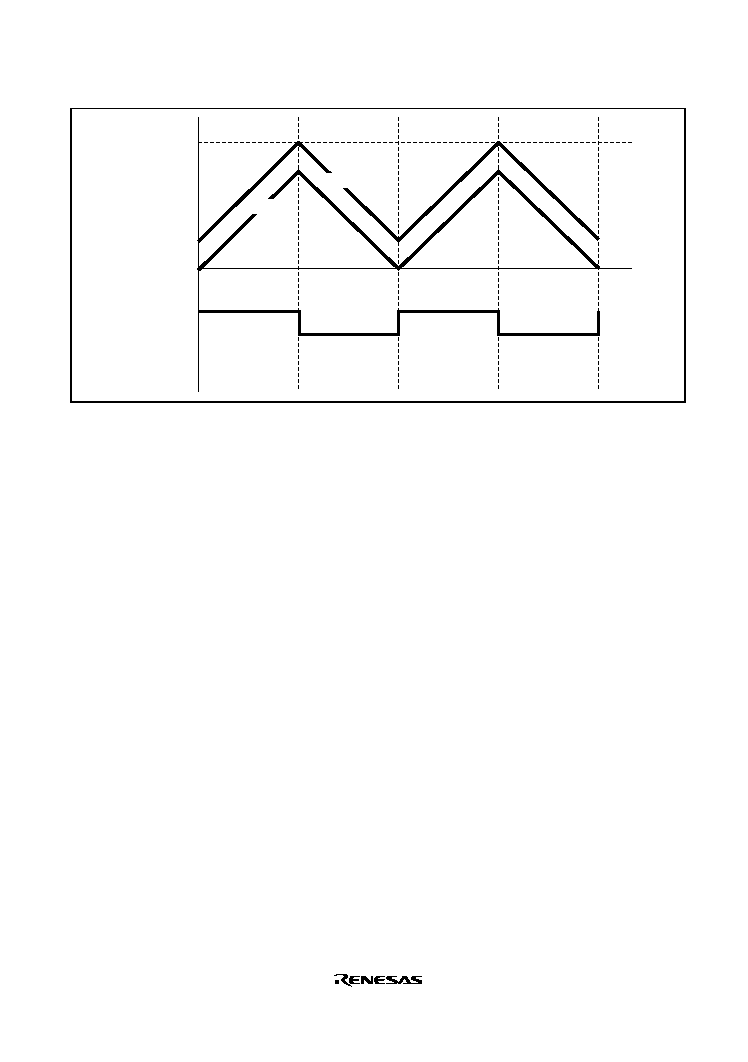
Rev. 2.0, 09/02, page 279 of 732
TGRA_3
H'0000
Toggle output
TIOC3A pin
TCNT_4
TCNT_3
Figure 11.48 Example of Toggle Output Waveform Synchronized with PWM Output
Counter Clearing by another Channel: In complementary PWM mode, by setting a mode for
synchronization with another channel by means of the timer synchronous register (TSYR), and
selecting synchronous clearing with bits CCLR2 to CCLR0 in the timer control register (TCR), it
is possible to have TCNT_3, TCNT_4, and TCNTS cleared by another channel.
Figure 11.49 illustrates the operation.
Use of this function enables counter clearing and restarting to be performed by means of an
external signal.
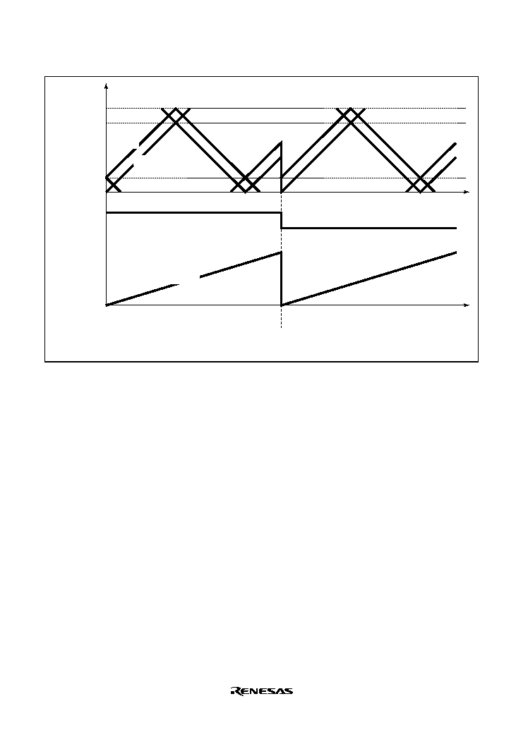
Rev. 2.0, 09/02, page 280 of 732
TGRA_3
TCDR
TDDR
H'0000
Channel 1
Input capture A
TCNT_1
TCNT_3
TCNT_4
TCNTS
Synchronous counter clearing by channel 1 input capture A
Figure 11.49 Counter Clearing Synchronized with Another Channel
Example of AC Synchronous Motor (Brushless DC Motor) Drive Waveform Output: In
complementary PWM mode, a brushless DC motor can easily be controlled using the timer gate
control register (TGCR). Figures 11.50 to 11.53 show examples of brushless DC motor drive
waveforms created using TGCR.
When output phase switching for a 3-phase brushless DC motor is performed by means of external
signals detected with a Hall element, etc., clear the FB bit in TGCR to 0. In this case, the external
signals indicating the polarity position are input to channel 0 timer input pins TIOC0A, TIOC0B,
and TIOC0C (set with PFC). When an edge is detected at pin TIOC0A, TIOC0B, or TIOC0C, the
output on/off state is switched automatically.
When the FB bit is 1, the output on/off state is switched when the UF, VF, or WF bit in TGCR is
cleared to 0 or set to 1.
The drive waveforms are output from the complementary PWM mode 6-phase output pins. With
this 6-phase output, in the case of on output, it is possible to use complementary PWM mode
output and perform chopping output by setting the N bit or P bit to 1. When the N bit or P bit is 0,
level output is selected.
The 6-phase output active level (on output level) can be set with the OLSN and OLSP bits in the
timer output control register (TOCR) regardless of the setting of the N and P bits.
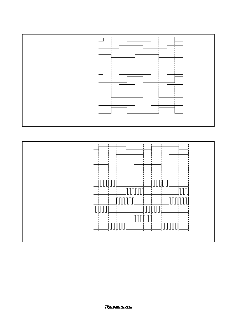
Rev. 2.0, 09/02, page 281 of 732
External input
TIOC0A pin
TIOC0B pin
TIOC0C pin
TIOC3B pin
TIOC3D pin
TIOC4A pin
TIOC4C pin
TIOC4B pin
TIOC4D pin
6-phase output
When BDC = 1, N = 0, P = 0, FB = 0, output active level = high
Figure 11.50 Example of Output Phase Switching by External Input (1)
External input
TIOC0A pin
TIOC0B pin
TIOC0C pin
TIOC3B pin
TIOC3D pin
TIOC4A pin
TIOC4C pin
TIOC4B pin
TIOC4D pin
6-phase output
When BDC = 1, N = 1, P = 1, FB = 0, output active level = high
Figure 11.51 Example of Output Phase Switching by External Input (2)
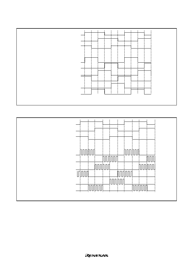
Rev. 2.0, 09/02, page 282 of 732
TGCR
UF bit
VF bit
WF bit
TIOC3B pin
TIOC3D pin
TIOC4A pin
TIOC4C pin
TIOC4B pin
TIOC4D pin
6-phase output
When BDC = 1, N = 0, P = 0, FB = 1, output active level = high
Figure 11.52 Example of Output Phase Switching by Means of UF, VF, WF Bit Settings (1)
TGCR
UF bit
VF bit
WF bit
TIOC3B pin
TIOC3D pin
TIOC4A pin
TIOC4C pin
TIOC4B pin
TIOC4D pin
6-phase output
When BDC = 1, N = 1, P = 1, FB = 1, output active level = high
Figure 11.53 Example of Output Phase Switching by Means of UF, VF, WF Bit Settings (2)

Rev. 2.0, 09/02, page 283 of 732
A/D Conversion Start Request Setting: In complementary PWM mode, an A/D conversion start
request can be issued using a TGRA_3 compare-match or a compare-match on a channel other
than channels 3 and 4.
When start requests using a TGRA_3 compare-match are set, A/D conversion can be started at the
center of the PWM pulse.
A/D conversion start requests can be set by setting the TTGE bit to 1 in the timer interrupt enable
register (TIER).
Complementary PWM Mode Output Protection Function
Complementary PWM mode output has the following protection functions.
∑
Register and counter miswrite prevention function
With the exception of the buffer registers, which can be rewritten at any time, access by the CPU
can be enabled or disabled for the mode registers, control registers, compare registers, and
counters used in complementary PWM mode by means of the MTURWE bit in the bus
controller's bus control register 1 (BCR1). The applicable registers are some (21 in total) of the
registers in channels 3 and 4 shown in the following:
TCR_3 and TCR_4, TMDR_3 and TMDR_4, TIORH_3 and TIORH_4, TIORL_3 and
TIORL_4, TIER_3 and TIER_4, TCNT_3 and TCNT_4, TGRA_3 and TGRA_4, TGRB_3
and TGRB_4, TOER, TOCR, TGCR, TCDR, and TDDR.
This function enables miswriting due to CPU runaway to be prevented by disabling CPU access to
the mode registers, control registers, and counters.
When the applicable registers are read in the
access-disabled state, undefined values are returned. Writing to these registers is ignored.
∑
Halting of PWM output by external signal
The 6-phase PWM output pins can be set automatically to the high-impedance state by
inputting specified external signals. There are four external signal input pins.
See section 11.9, Port Output Enable (POE), for details.
∑
Halting of PWM output when oscillator is stopped
If it is detected that the clock input to this LSI has stopped, the 6-phase PWM output pins
automatically go to the high-impedance state. The pin states are not guaranteed when the clock
is restarted.
See section 4.2, Function for Detecting the Oscillator Halt.

Rev. 2.0, 09/02, page 284 of 732
11.5
Interrupt Sources
11.5.1
Interrupt Sources and Priorities
There are three kinds of MTU interrupt source; TGR input capture/compare match, TCNT
overflow, and TCNT underflow. Each interrupt source has its own status flag and enable/disabled
bit, allowing the generation of interrupt request signals to be enabled or disabled individually.
When an interrupt request is generated, the corresponding status flag in TSR is set to 1. If the
corresponding enable/disable bit in TIER is set to 1 at this time, an interrupt is requested. The
interrupt request is cleared by clearing the status flag to 0.
Relative channel priorities can be changed by the interrupt controller, however the priority order
within a channel is fixed. For details, see section 6, Interrupt Controller.
Table 11.42 lists the MTU interrupt sources.

Rev. 2.0, 09/02, page 285 of 732
Table 11.42 MTU Interrupts
Channel
Name
Interrupt Source
Interrupt
Flag
DMAC
Activation
DTC
Activation
Priority
0
TGIA_0
TGRA_0 input capture/compare match TGFA_0
Possible
Possible
High
TGIB_0
TGRB_0 input capture/compare match TGFB_0
Not possible Possible
TGIC_0 TGRC_0 input capture/compare match TGFC_0
Not possible Possible
TGID_0 TGRD_0 input capture/compare match TGFD_0
Not possible Possible
TCIV_0
TCNT_0 overflow
TCFV_0
Not possible Not possible
1
TGIA_1
TGRA_1 input capture/compare match TGFA_1
Possible
Possible
TGIB_1
TGRB_1 input capture/compare match TGFB_1
Not possible Possible
TCIV_1
TCNT_1 overflow
TCFV_1
Not possible Not possible
TCIU_1
TCNT_1 underflow
TCFU_1
Not possible Not possible
2
TGIA_2
TGRA_2 input capture/compare match TGFA_2
Possible
Possible
TGIB_2
TGRB_2 input capture/compare match TGFB_2
Not possible Possible
TCIV_2
TCNT_2 overflow
TCFV_2
Not possible Not possible
TCIU_2
TCNT_2 underflow
TCFU_2
Not possible Not possible
3
TGIA_3
TGRA_3 input capture/compare match TGFA_3
Possible
Possible
TGIB_3
TGRB_3 input capture/compare match TGFB_3
Not possible Possible
TGIC_3 TGRC_3 input capture/compare match TGFC_3
Not possible Possible
TGID_3 TGRD_3 input capture/compare match TGFD_3
Not possible Possible
TCIV_3
TCNT_3 overflow
TCFV_3
Not possible Not possible
4
TGIA_4
TGRA_4 input capture/compare match TGFA_4
Possible
Possible
TGIB_4
TGRB_4 input capture/compare match TGFB_4
Not possible Possible
TGIC_4 TGRC_4 input capture/compare match TGFC_4
Not possible Possible
TGID_4 TGRD_4 input capture/compare match TGFD_4
Not possible Possible
TCIV_4
TCNT_4 overflow/underflow
TCFV_4
Not possible Possible
Low
Note:
This table shows the initial state immediately after a reset. The relative channel priorities
can be changed by the interrupt controller.

Rev. 2.0, 09/02, page 286 of 732
Input Capture/Compare Match Interrupt: An interrupt is requested if the TGIE bit in TIER is
set to 1 when the TGF flag in TSR is set to 1 by the occurrence of a TGR input capture/compare
match on a particular channel. The interrupt request is cleared by clearing the TGF flag to 0. The
MTU has 16 input capture/compare match interrupts, four each for channels 0, 3, and 4, and two
each for channels 1 and 2.
Overflow Interrupt: An interrupt is requested if the TCIEV bit in TIER is set to 1 when the
TCFV flag in TSR is set to 1 by the occurrence of TCNT overflow on a channel. The interrupt
request is cleared by clearing the TCFV flag to 0. The MTU has five overflow interrupts, one for
each channel.
Underflow Interrupt: An interrupt is requested if the TCIEU bit in TIER is set to 1 when the
TCFU flag in TSR is set to 1 by the occurrence of TCNT underflow on a channel. The interrupt
request is cleared by clearing the TCFU flag to 0. The MTU has two underflow interrupts, one
each for channels 1 and 2.
11.5.2
DTC/DMAC Activation
DTC Activation: The DTC can be activated by the TGR input capture/compare match interrupt in
each channel. For details, see section 8, Data Transfer Controller (DTC).
A total of 17 MTU input capture/compare match interrupts can be used as DTC activation sources,
four each for channels 0 and 3, and two each for channels 1 and 2, and five for channel 4.
DMAC Activation: The DMAC can be activated by the TGRA input capture/compare match
interrupt in each channel. For details, see section 10, Direct Memory Access Controller (DMAC).
A total of five MTU input capture/compare match interrupts can be used as DMAC activation
sources, one for each channel.
11.5.3
A/D Converter Activation
The A/D converter can be activated by the TGRA input capture/compare match in each channel.
If the TTGE bit in TIER is set to 1 when the TGFA flag in TSR is set to 1 by the occurrence of a
TGRA input capture/compare match on a particular channel, a request to start A/D conversion is
sent to the A/D converter. If the MTU conversion start trigger has been selected on the A/D
converter at this time, A/D conversion starts.
In the MTU, a total of five TGRA input capture/compare match interrupts can be used as A/D
converter conversion start sources, one for each channel.
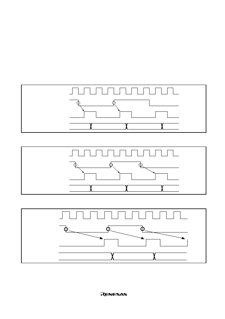
Rev. 2.0, 09/02, page 287 of 732
11.6
Operation Timing
11.6.1
Input/Output Timing
TCNT Count Timing: Figure 11.54 shows TCNT count timing in internal clock operation, and
figure 11.55 shows TCNT count timing in external clock operation (normal mode), and figure
11.56 shows TCNT count timing in external clock operation (phase counting mode).
TCNT
TCNT input
clock
Internal clock
P
N-1
N
N+1
N+2
Falling edge
Rising edge
Figure 11.54 Count Timing in Internal Clock Operation
TCNT
TCNT input
clock
External clock
P
N-1
N
N+1
N+2
Falling edge
Rising edge
Falling edge
Figure 11.55 Count Timing in External Clock Operation
P
External
clock
TCNT input
clock
TCNT
Falling edge
Falling edge
Rising edge
N-1
N
N+1
Figure 11.56 Count Timing in External Clock Operation (Phase Counting Mode)
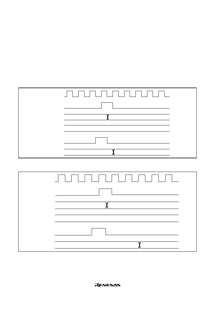
Rev. 2.0, 09/02, page 288 of 732
Output Compare Output Timing: A compare match signal is generated in the final state in
which TCNT and TGR match (the point at which the count value matched by TCNT is updated).
When a compare match signal is generated, the output value set in TIOR is output at the output
compare output pin (TIOC pin). After a match between TCNT and TGR, the compare match
signal is not generated until the TCNT input clock is generated.
Figure 11.57 shows output compare output timing (normal mode and PWM mode) and figure
11.58 shows output compare output timing (complementary PWM mode and reset synchronous
PWM mode).
TGR
TCNT
TCNT input
clock
N
N
N+1
Compare
match signal
TIOC pin
P
Figure 11.57 Output Compare Output Timing (Normal Mode/PWM Mode)
P
TCNT input
clock
TCNT
N
N+1
TGR
Compare
match signal
TIOC pin
N
Figure 11.58 Output Compare Output Timing (Complementary PWM Mode/Reset
Synchronous PWM Mode)
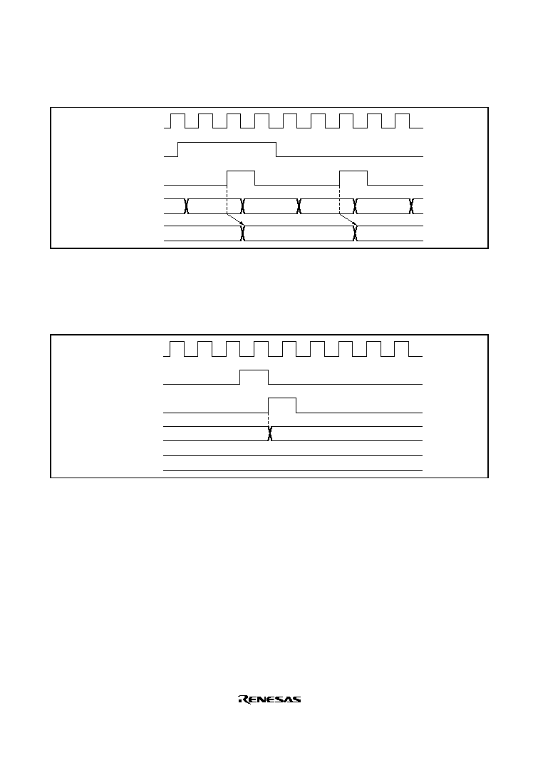
Rev. 2.0, 09/02, page 289 of 732
Input Capture Signal Timing: Figure 11.59 shows input capture signal timing.
TCNT
Input capture
input
N
N+1
N+2
N
N+2
TGR
Input capture
signal
P
Figure 11.59 Input Capture Input Signal Timing
Timing for Counter Clearing by Compare Match/Input Capture: Figure 11.60 shows the
timing when counter clearing on compare match is specified, and figure 11.61 shows the timing
when counter clearing on input capture is specified.
TCNT
Counter
clear signal
Compare
match signal
TGR
N
N
H'0000
P
Figure 11.60 Counter Clear Timing (Compare Match)
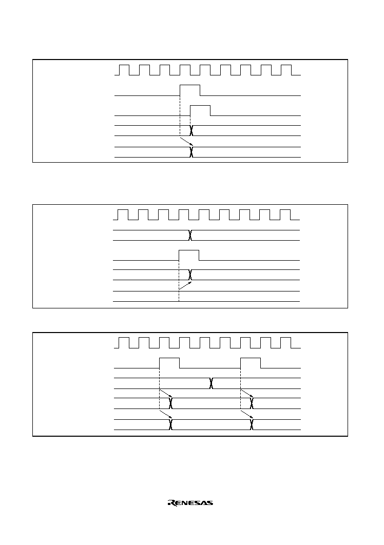
Rev. 2.0, 09/02, page 290 of 732
TCNT
Counter clear
signal
Input capture
signal
TGR
N
H'0000
N
P
Figure 11.61 Counter Clear Timing (Input Capture)
Buffer Operation Timing: Figures 11.62 and 11.63 show the timing in buffer operation.
TGRA,
TGRB
Compare
match buffer
signal
TCNT
TGRC,
TGRD
n
N
N
n
n+1
P
Figure 11.62 Buffer Operation Timing (Compare Match)
TGRA,
TGRB
TCNT
Input capture
signal
TGRC,
TGRD
N
n
n
N+1
N
N
N+1
P
Figure 11.63 Buffer Operation Timing (Input Capture)
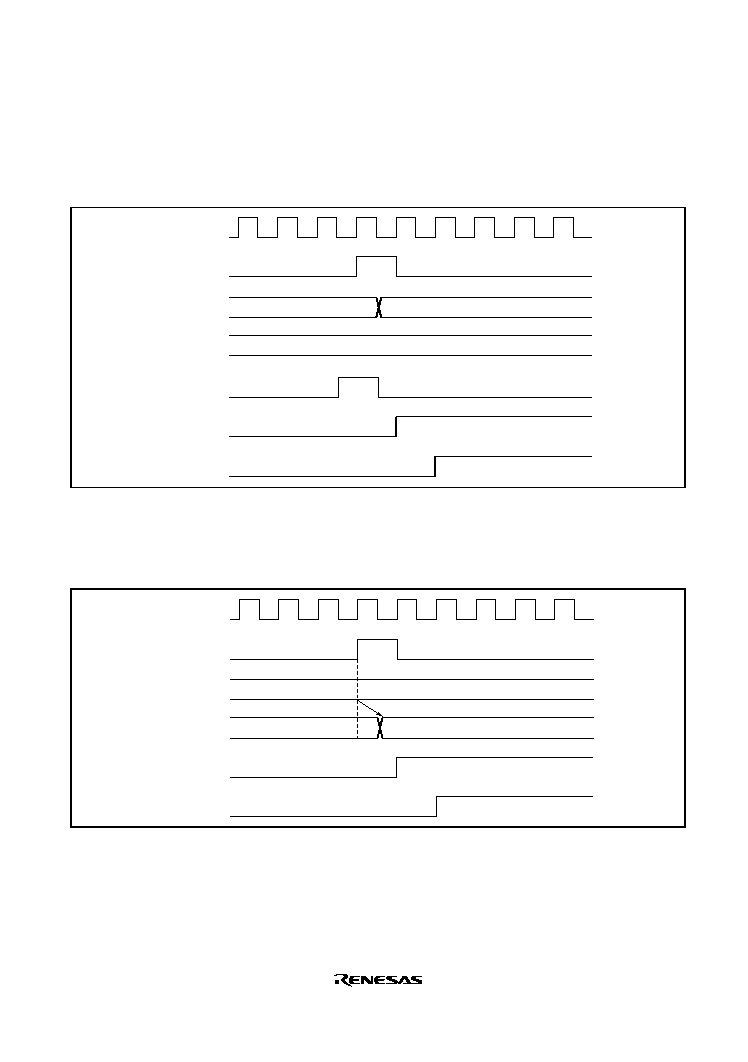
Rev. 2.0, 09/02, page 291 of 732
11.6.2
Interrupt Signal Timing
TGF Flag Setting Timing in Case of Compare Match: Figure 11.64 shows the timing for
setting of the TGF flag in TSR on compare match, and TGI interrupt request signal timing.
TGR
TCNT
TCNT input
clock
N
N
N+1
Compare
match signal
TGF flag
TGI interrupt
P
Figure 11.64 TGI Interrupt Timing (Compare Match)
TGF Flag Setting Timing in Case of Input Capture: Figure 11.65 shows the timing for setting
of the TGF flag in TSR on input capture, and TGI interrupt request signal timing.
TGR
TCNT
Input capture
signal
N
N
TGF flag
TGI interrupt
P
Figure 11.65 TGI Interrupt Timing (Input Capture)
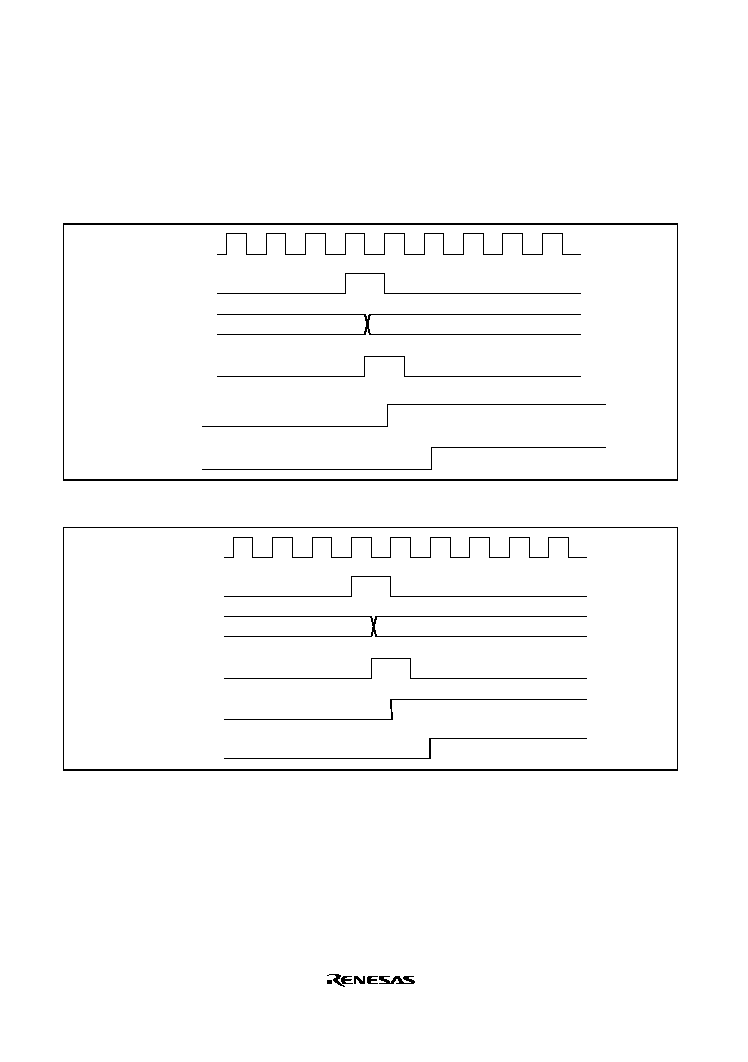
Rev. 2.0, 09/02, page 292 of 732
TCFV Flag/TCFU Flag Setting Timing: Figure 11.66 shows the timing for setting of the TCFV
flag in TSR on overflow, and TCIV interrupt request signal timing.
Figure 11.67 shows the timing for setting of the TCFU flag in TSR on underflow, and TCIU
interrupt request signal timing.
Overflow
signal
TCNT
(overflow)
TCNT input
clock
H'FFFF
H'0000
TCFV flag
TCIV interrupt
P
Figure 11.66 TCIV Interrupt Setting Timing
Underflow
signal
TCNT
(underflow)
TCNT
input clock
H'0000
H'FFFF
TCFU flag
TCIU interrupt
P
Figure 11.67 TCIU Interrupt Setting Timing
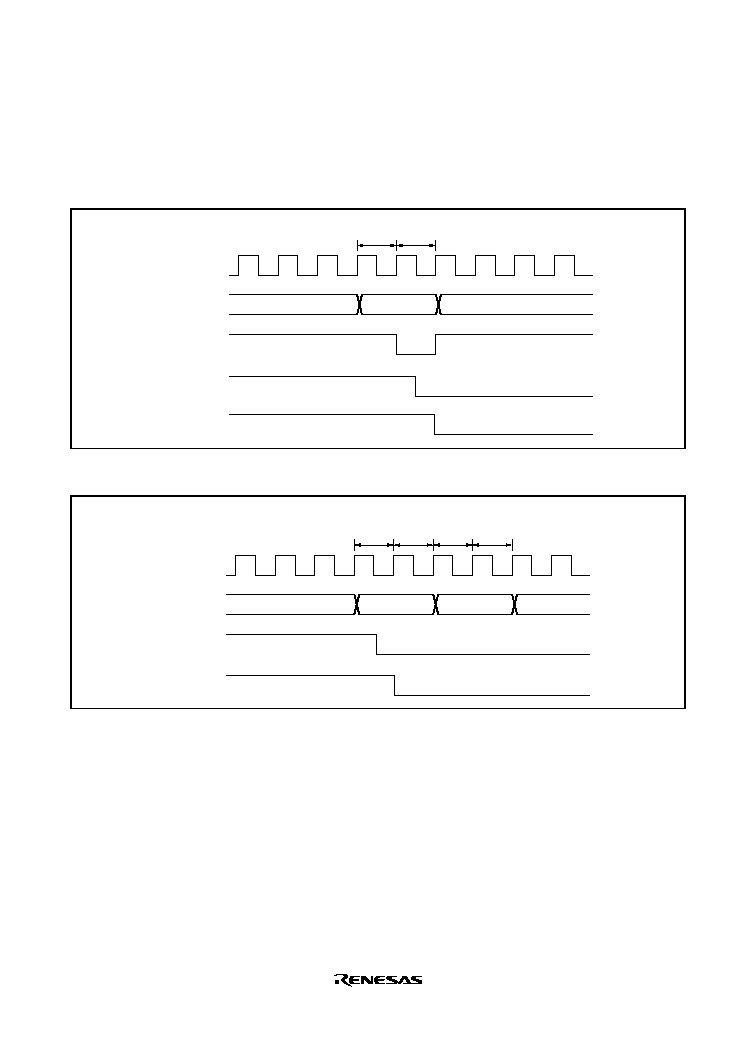
Rev. 2.0, 09/02, page 293 of 732
Status Flag Clearing Timing: After a status flag is read as 1 by the CPU, it is cleared by writing
0 to it. When the DTC/DMAC is activated, the flag is cleared automatically. Figure 11.68 shows
the timing for status flag clearing by the CPU, and figure 11.69 shows the timing for status flag
clearing by the DTC/DMAC.
Status flag
Write signal
Address
TSR address
Interrupt
request signal
TSR write cycle
T1
T2
P
Figure 11.68 Timing for Status Flag Clearing by the CPU
Interrupt
request signal
Status flag
Address
Source address
DTC/DMAC
read cycle
T1
T2
Destination
address
T1
T2
DTC/DMAC
write cycle
P
Figure 11.69 Timing for Status Flag Clearing by DTC/DMAC Activation
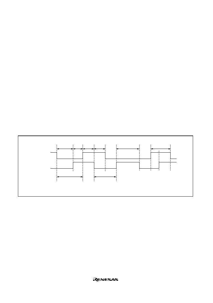
Rev. 2.0, 09/02, page 294 of 732
11.7
Usage Notes
11.7.1
Module Standby Mode Setting
MTU operation can be disabled or enabled using the module standby register. The initial setting is
for MTU operation to be halted. Register access is enabled by clearing module standby mode. For
details, refer to section 24, Power-Down Modes.
11.7.2
Input Clock Restrictions
The input clock pulse width must be at least 1.5 states in the case of single-edge detection, and at
least 2.5 states in the case of both-edge detection. The MTU will not operate properly at narrower
pulse widths.
In phase counting mode, the phase difference and overlap between the two input clocks must be at
least 1.5 states, and the pulse width must be at least 2.5 states. Figure 11.70 shows the input clock
conditions in phase counting mode.
Overlap
Phase
differ-
ence
Phase
differ-
ence
Overlap
TCLKA
(TCLKC)
TCLKB
(TCLKD)
Pulse width
Pulse width
Pulse width
Pulse width
Notes: Phase difference and overlap
Pulse width
: 1.5 states or more
: 2.5 states or more
Figure 11.70 Phase Difference, Overlap, and Pulse Width in Phase Counting Mode
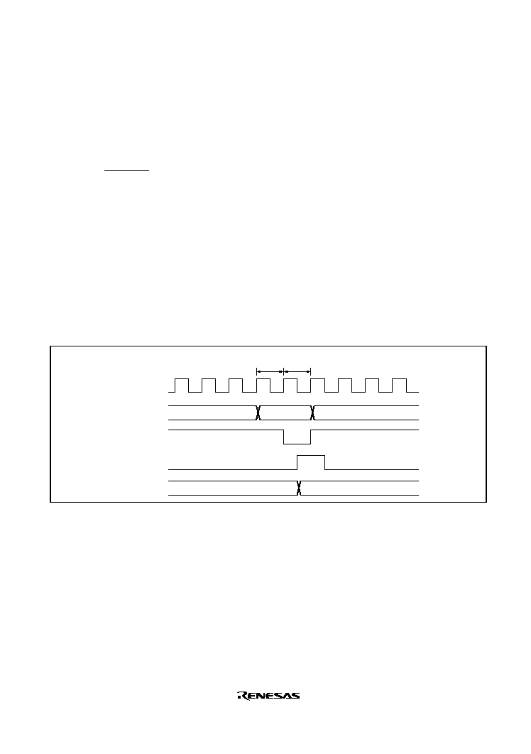
Rev. 2.0, 09/02, page 295 of 732
11.7.3
Caution on Period Setting
When counter clearing on compare match is set, TCNT is cleared in the final state in which it
matches the TGR value (the point at which the count value matched by TCNT is updated).
Consequently, the actual counter frequency is given by the following formula:
f =
P
(N + 1)
Where
f
: Counter frequency
P
: Peripheral clock operating frequency
N
: TGR set value
11.7.4
Contention between TCNT Write and Clear Operations
If the counter clear signal is generated in the T2 state of a TCNT write cycle, TCNT clearing takes
precedence and the TCNT write is not performed.
Figure 11.71 shows the timing in this case.
Counter clear
signal
Write signal
Address
P
TCNT address
TCNT
TCNT write cycle
T1
T2
N
H'0000
Figure 11.71 Contention between TCNT Write and Clear Operations
11.7.5
Contention between TCNT Write and Increment Operations
If incrementing occurs in the T2 state of a TCNT write cycle, the TCNT write takes precedence
and TCNT is not incremented.
Figure 11.72 shows the timing in this case.
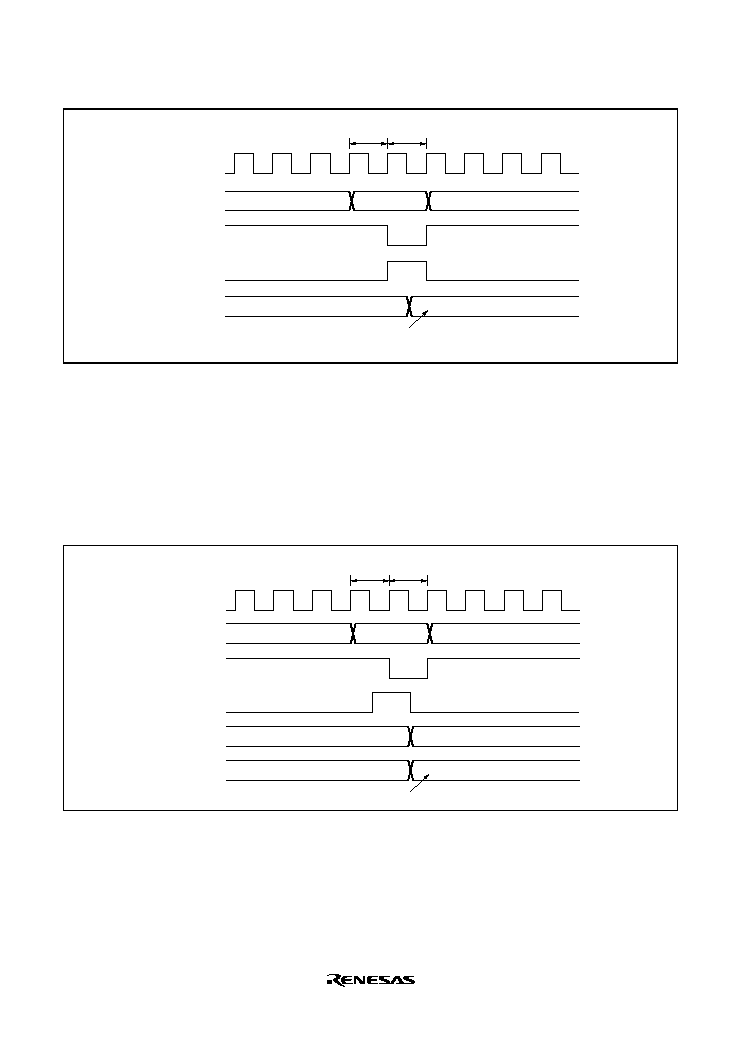
Rev. 2.0, 09/02, page 296 of 732
TCNT input
clock
Write signal
Address
P
TCNT address
TCNT
TCNT write cycle
T1
T2
N
M
TCNT write data
Figure 11.72 Contention between TCNT Write and Increment Operations
11.7.6
Contention between TGR Write and Compare Match
If a compare match occurs in the T2 state of a TGR write cycle, the TGR write is executed and the
compare match signal is also generated.
Figure 11.73 shows the timing in this case.
Compare
match signal
Write signal
Address
P
TGR address
TCNT
TGR write cycle
T1
T2
N
M
TGR write data
TGR
N
N+1
Figure 11.73 Contention between TGR Write and Compare Match
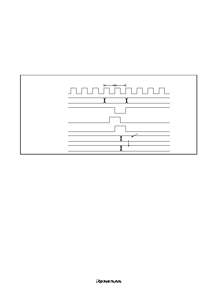
Rev. 2.0, 09/02, page 297 of 732
11.7.7
Contention between Buffer Register Write and Compare Match
If a compare match occurs in the T2 state of a TGR write cycle, the data that is transferred to TGR
by the buffer operation differs depending on channel 0 and channels 3 and 4: data on channel 0 is
that after write, and on channels 3 and 4, before write.
Figures 11.74 and 11.75 show the timing in this case.
Compare match
buffer signal
Write signal
Address
P
Buffer register
address
Buffer register
TGR write cycle
T1
T2
Compare
match signal
TGR
N
M
M
Buffer register write data
Figure 11.74 Contention between Buffer Register Write and Compare Match (Channel 0)
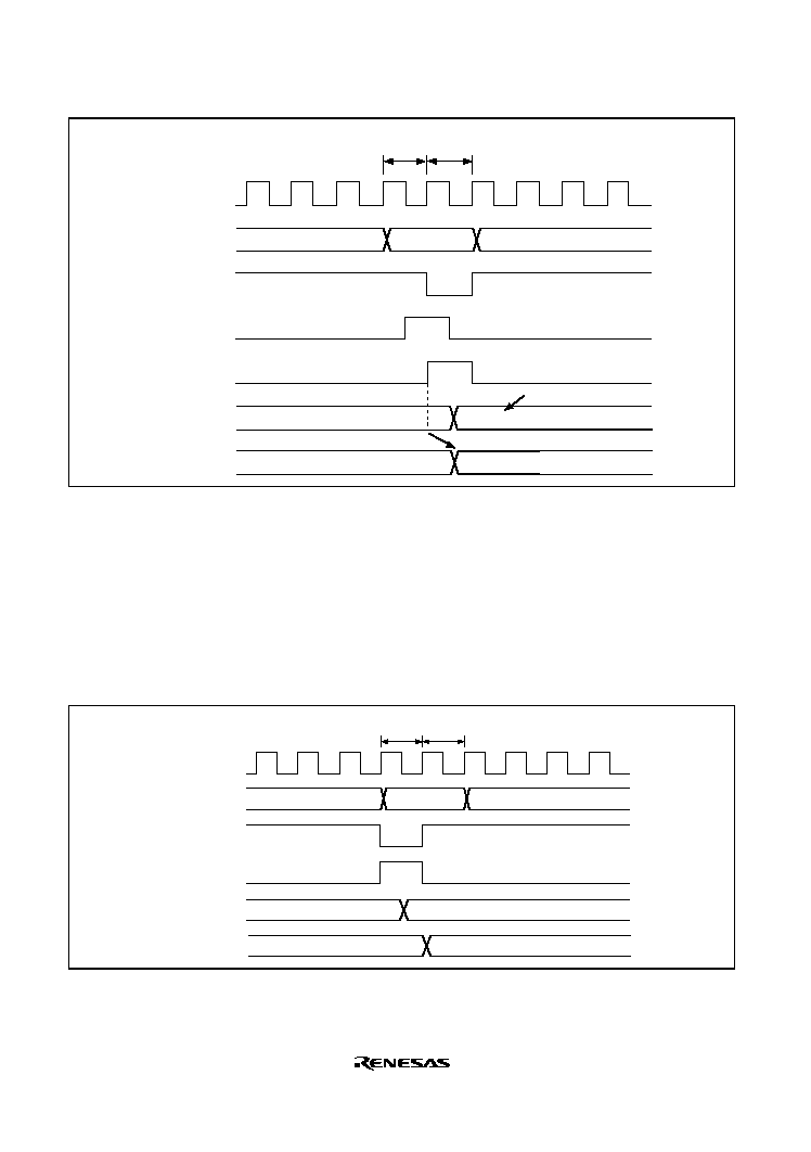
Rev. 2.0, 09/02, page 298 of 732
P
Address
Write signal
Compare match
signal
Compare match
buffer signal
TGR write cycle
T1
T2
Buffer register
address
N
N
M
Buffer register write data
Buffer register
TGR
Figure 11.75 Contention between Buffer Register Write and Compare Match
(Channels 3 and 4)
11.7.8
Contention between TGR Read and Input Capture
If an input capture signal is generated in the T1 state of a TGR read cycle, the data that is read will
be that in the buffer after input capture transfer.
Figure 11.76 shows the timing in this case.
Input capture
signal
Read signal
Address
P
TGR read cycle
T1
T2
TGR
X
M
M
Internal data
bus
TGR address
Figure 11.76 Contention between TGR Read and Input Capture
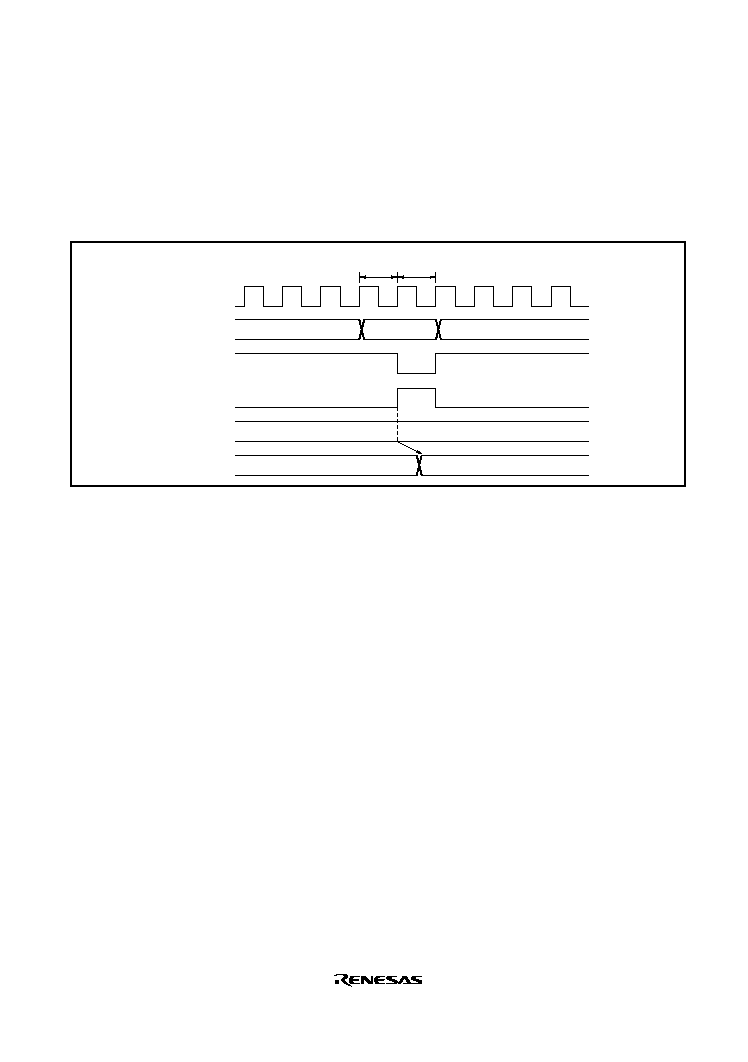
Rev. 2.0, 09/02, page 299 of 732
11.7.9
Contention between TGR Write and Input Capture
If an input capture signal is generated in the T2 state of a TGR write cycle, the input capture
operation takes precedence and the write to TGR is not performed.
Figure 11.77 shows the timing in this case.
Input capture
signal
Write signal
Address
P
TCNT
TGR write cycle
T1
T2
M
TGR
M
TGR address
Figure 11.77 Contention between TGR Write and Input Capture
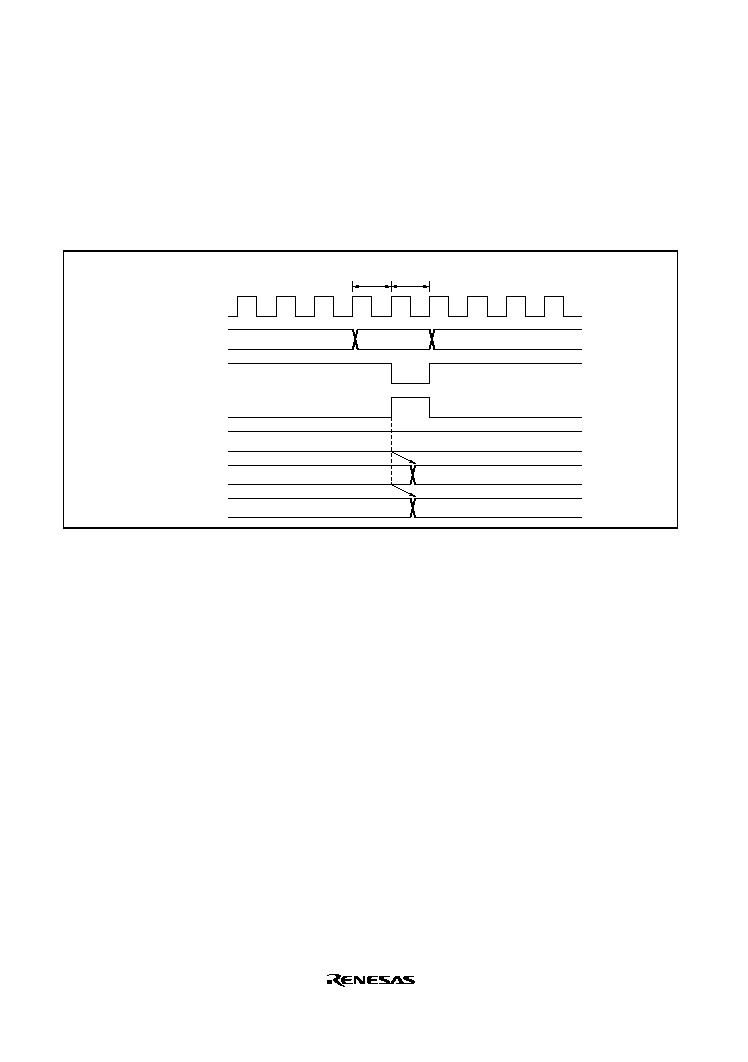
Rev. 2.0, 09/02, page 300 of 732
11.7.10
Contention between Buffer Register Write and Input Capture
If an input capture signal is generated in the T2 state of a buffer register write cycle, the buffer
operation takes precedence and the write to the buffer register is not performed.
Figure 11.78 shows the timing in this case.
Input capture
signal
Write signal
Address
P
TCNT
Buffer register write cycle
T1
T2
N
TGR
N
M
M
Buffer register
Buffer register
address
Figure 11.78 Contention between Buffer Register Write and Input Capture
11.7.11
TCNT2 Write and Overflow/Underflow Contention in Cascade Connection
With timer counters TCNT1 and TCNT2 in a cascade connection, when a contention occurs
during TCNT_1 count (during a TCNT_2 overflow/underflow) in the T
2
state of the TCNT_2
write cycle, the write to TCNT_2 is conducted, and the TCNT_1 count signal is disabled. At this
point, if there is match with TGRA_1 and the TCNT_1 value, a compare signal is issued.
Furthermore, when the TCNT_1 count clock is selected as the input capture source of channel 0,
TGRA_0 to D_0 carry out the input capture operation. In addition, when the compare match/input
capture is selected as the input capture source of TGRB_1, TGRB_1 carries out input capture
operation. The timing is shown in figure 11.79.
For cascade connections, be sure to synchronize settings for channels 1 and 2 when setting TCNT
clearing.
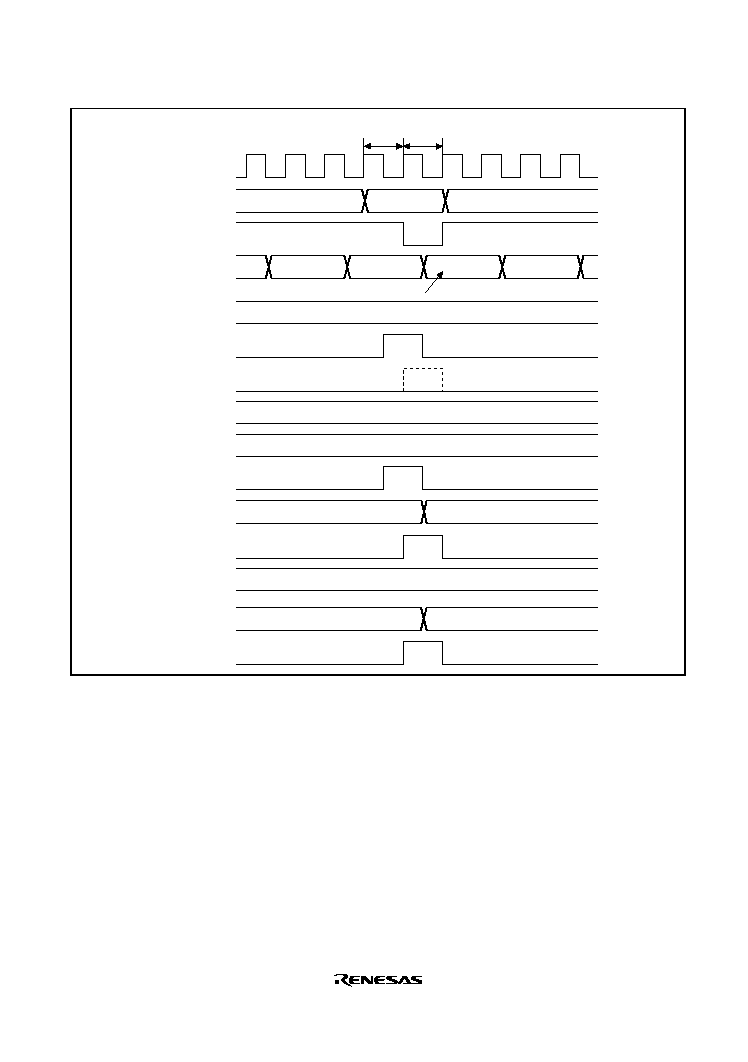
Rev. 2.0, 09/02, page 301 of 732
T1
T2
H'FFFE
H'FFFF
N
N + 1
H'FFFF
M
M
N
P
Q
P
M
Disabled
TCNT_2 write data
TCNT_2 address
TCNT write cycle
P
Address
Write signal
TCNT_2
TGRA_2 to
TGRB_2
Ch2 compare-
match signal A/B
TCNT_1 input
clock
TCNT_1
TGRA_1
Ch1 compare-
match signal A
TGRB_1
Ch1 input capture
signal B
TCNT_0
TGRA_0 to
TGRD_0
Ch0 input capture
signal A to D
Figure 11.79 TCNT_2 Write and Overflow/Underflow Contention with Cascade
Connection
11.7.12
Counter Value during Complementary PWM Mode Stop
When counting operation is suspended with TCNT_3 and TCNT_4 in complementary PWM
mode, TCNT_3 has the timer dead time register (TDDR) value, and TCNT_4 is held at H'0000.
When restarting complementary PWM mode, counting begins automatically from the initialized
state. This explanatory diagram is shown in figure 11.80.
When counting begins in another operating mode, be sure that TCNT_3 and TCNT_4 are set to
the initial values.
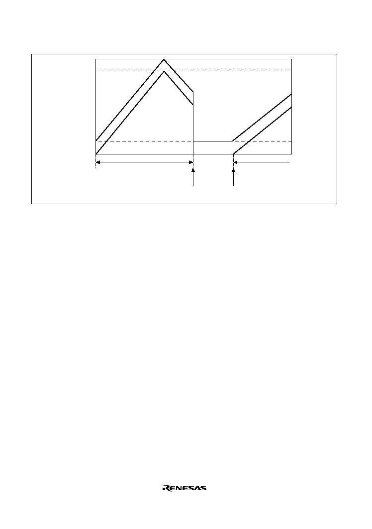
Rev. 2.0, 09/02, page 302 of 732
TGRA_3
TCDR
TDDR
H'0000
TCNT_3
TCNT_4
Complementary PWM
mode operation
Complementary PWM
mode operation
Counter
operation stop
Complementary
PMW restart
Figure 11.80 Counter Value during Complementary PWM Mode Stop
11.7.13
Buffer Operation Setting in Complementary PWM Mode
In complementary PWM mode, conduct rewrites by buffer operation for the PWM cycle setting
register (TGRA_3), timer cycle data register (TCDR), and duty setting registers (TGRB_3,
TGRA_4, and TGRB_4).
In complementary PWM mode, channel 3 and channel 4 buffers operate in accordance with bit
settings BFA and BFB of TMDR_3. When TMDR_3's BFA bit is set to 1, TGRC_3 functions as a
buffer register for TGRA_3. At the same time, TGRC_4 functions as the buffer register for
TGRA_4, while the TCBR functions as the TCDR's buffer register.
11.7.14
Reset Sync PWM Mode Buffer Operation and Compare Match Flag
When setting buffer operation for reset sync PWM mode, set the BFA and BFB bits of TMDR_4
to 0. The TIOC4C pin will be unable to produce its waveform output if the BFA bit of TMDR_4 is
set to 1.
In reset sync PWM mode, the channel 3 and channel 4 buffers operate in accordance with the BFA
and BFB bit settings of TMDR_3. For example, if the BFA bit of TMDR_3 is set to 1, TGRC_3
functions as the buffer register for TGRA_3. At the same time, TGRC_4 functions as the buffer
register for TGRA_4.
The TGFC bit and TGFD bit of TSR_3 and TSR_4 are not set when TGRC_3 and TGRD_3 are
operating as buffer registers.
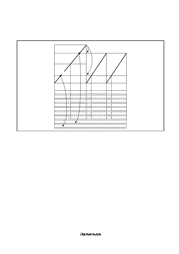
Rev. 2.0, 09/02, page 303 of 732
Figure 11.81 shows an example of operations for TGR_3, TGR_4, TIOC3, and TIOC4, with
TMDR_3's BFA and BFB bits set to 1, and TMDR_4's BFA and BFB bits set to 0.
TGRA_3
TGRC_3
TGRB_3, TGRA_4,
TGRB_4
TGRD_3, TGRC_4,
TGRD_4
H'0000
TIOC3A
TIOC3B
TIOC3D
TIOC4A
TIOC4C
TIOC4B
TIOC4D
TGFC
TGFD
TGRA_3,
TGRC_3
TGRB_3, TGRD_3,
TGRA_4, TGRC_4,
TGRB_4, TGRD_4
Buffer transfer with
compare match A3
TCNT3
Not set
Not set
Point a
Point b
Figure 11.81 Buffer Operation and Compare-Match Flags in Reset Sync PWM Mode
11.7.15
Overflow Flags in Reset Synchronous PWM Mode
When set to reset synchronous PWM mode, TCNT_3 and TCNT_4 start counting when the CST3
bit of TSTR is set to 1. At this point, TCNT_4's count clock source and count edge obey the
TCR_3 setting.
In reset synchronous PWM mode, with cycle register TGRA_3's set value at H'FFFF, when
specifying TGR3A compare-match for the counter clear source, TCNT_3 and TCNT_4 count up
to H'FFFF, then a compare-match occurs with TGRA_3, and TCNT_3 and TCNT_4 are both
cleared. At this point, TSR's overflow flag TCFV bit is not set.
Figure 11.82 shows a TCFV bit operation example in reset synchronous PWM mode with a set
value for cycle register TGRA_3 of H'FFFF, when a TGRA_3 compare-match has been specified
without synchronous setting for the counter clear source.
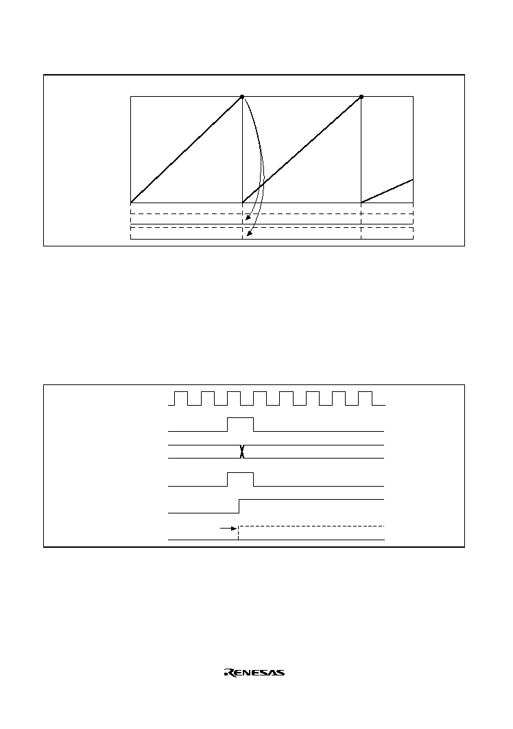
Rev. 2.0, 09/02, page 304 of 732
TGRA_3
(H'FFFF)
H'0000
TCFV_3
TCFV_4
TCNT_3 = TCNT_4
Counter cleared by compare match 3A
Not set
Not set
Figure 11.82 Reset Synchronous PWM Mode Overflow Flag
11.7.16
Contention between Overflow/Underflow and Counter Clearing
If overflow/underflow and counter clearing occur simultaneously, the TCFV/TCFU flag in TSR is
not set and TCNT clearing takes precedence.
Figure 11.83 shows the operation timing when a TGR compare match is specified as the clearing
source, and when H'FFFF is set in TGR.
Counter clear
signal
TCNT
TCNT input
clock
P
H'FFFF
H'0000
TGF
TCFV
Disabled
Figure 11.83 Contention between Overflow and Counter Clearing

Rev. 2.0, 09/02, page 305 of 732
11.7.17
Contention between TCNT Write and Overflow/Underflow
If there is an up-count or down-count in the T2 state of a TCNT write cycle, and
overflow/underflow occurs, the TCNT write takes precedence and the TCFV/TCFU flag in TSR is
not set.
Figure 11.84 shows the operation timing when there is contention between TCNT write and
overflow.
Write signal
Address
P
TCNT address
TCNT
TCNT write cycle
T1
T2
H'FFFF
M
TCNT write data
TCFV flag
Figure 11.84 Contention between TCNT Write and Overflow
11.7.18
Cautions on Transition from Normal Operation or PWM Mode 1 to Reset-
Synchronous PWM Mode
When making a transition from channel 3 or 4 normal operation or PWM mode 1 to reset-
synchronous PWM mode, if the counter is halted with the output pins (TIOC3B, TIOC3D,
TIOC4A, TIOC4C, TIOC4B, TIOC4D) in the high-impedance state, followed by the transition to
reset-synchronous PWM mode and operation in that mode, the initial pin output will not be
correct.
When making a transition from normal operation to reset-synchronous PWM mode, write H'11 to
registers TIORH_3, TIORL_3, TIORH_4, and TIORL_4 to initialize the output pins to low level
output, then set an initial register value of H'00 before making the mode transition.
When making a transition from PWM mode 1 to reset-synchronous PWM mode, first switch to
normal operation, then initialize the output pins to low level output and set an initial register value
of H'00 before making the transition to reset-synchronous PWM mode.

Rev. 2.0, 09/02, page 306 of 732
11.7.19
Output Level in Complementary PWM Mode and Reset-Synchronous PWM Mode
When channels 3 and 4 are in complementary PWM mode or reset-synchronous PWM mode, the
PWM waveform output level is set with the OLSP and OLSN bits in the timer output control
register (TOCR). In the case of complementary PWM mode or reset-synchronous PWM mode,
TIOR should be set to H'00.
11.7.20
Interrupts in Module Standby Mode
If module standby mode is entered when an interrupt has been requested, it will not be possible to
clear the CPU interrupt source or the DTC/DMAC activation source. Interrupts should therefore
be disabled before entering module standby mode.
11.7.21
Simultaneous Capture of TCNT_1 and TCNT_2 in Cascade Connection
When timer counters 1 and 2 (TCNT_1 and TCNT_2) are operated as a 32-bit counter in cascade
connection, the cascade counter value cannot be captured successfully even if input-capture input
is simultaneously done to TIOC1A and TIOC2A or to TIOC1B and TIOC2B. This is because the
input timing of TIOC1A and TIOC2A or of TIOC1B and TIOC2B may not be the same when
external input-capture signals to be input into TCNT_1 and TCNT_2 are taken in synchronization
with the internal clock. For example, TCNT_1 (the counter for upper 16 bits) does not capture the
count-up value by overflow from TCNT_2 (the counter for lower 16 bits) but captures the count
value before the count-up. In this case, the values of TCNT_1 = H
FFF1 and TCNT_2 = H
0000
should be transferred to TGRA_1 and TGRA_2 or to TGRB_1 and TGRB_2, but the values of
TCNT_1 = H
FFF0 and TCNT_2 = H
0000 are erroneously transferred.
11.8
MTU Output Pin Initialization
11.8.1
Operating Modes
The MTU has the following six operating modes. Waveform output is possible in all of these
modes.
∑
Normal mode (channels 0 to 4)
∑
PWM mode 1 (channels 0 to 4)
∑
PWM mode 2 (channels 0 to 2)
∑
Phase counting modes 1 to 4 (channels 1 and 2)
∑
Complementary PWM mode (channels 3 and 4)
∑
Reset-synchronous PWM mode (channels 3 and 4)
The MTU output pin initialization method for each of these modes is described in this section.

Rev. 2.0, 09/02, page 307 of 732
11.8.2
Reset Start Operation
The MTU output pins (TIOC*) are initialized low by a reset and in standby mode. Since MTU pin
function selection is performed by the pin function controller (PFC), when the PFC is set, the
MTU pin states at that point are output to the ports. When MTU output is selected by the PFC
immediately after a reset, the MTU output initial level, low, is output directly at the port. When
the active level is low, the system will operate at this point, and therefore the PFC setting should
be made after initialization of the MTU output pins is completed.
Note:
Channel number and port notation are substituted for *.
11.8.3
Operation in Case of Re-Setting Due to Error During Operation, Etc.
If an error occurs during MTU operation, MTU output should be cut by the system. Cutoff is
performed by switching the pin output to port output with the PFC and outputting the inverse of
the active level. For large-current pins, output can also be cut by hardware, using port output
enable (POE). The pin initialization procedures for re-setting due to an error during operation, etc.,
and the procedures for restarting in a different mode after re-setting, are shown below.
The MTU has six operating modes, as stated above. There are thus 36 mode transition
combinations, but some transitions are not available with certain channel and mode combinations.
Possible mode transition combinations are shown in table 11.43.
Table 11.43 Mode Transition Combinations
After
Before
Normal
PWM1
PWM2
PCM
CPWM
RPWM
Normal
(1)
(2)
(3)
(4)
(5)
(6)
PWM1
(7)
(8)
(9)
(10)
(11)
(12)
PWM2
(13)
(14)
(15)
(16)
None
None
PCM
(17)
(18)
(19)
(20)
None
None
CPWM
(21)
(22)
None
None
(23) (24)
(25)
RPWM
(26)
(27)
None
None
(28)
(29)
Legend:
Normal: Normal mode
PWM1: PWM mode 1
PWM2: PWM mode 2
PCM:
Phase counting modes 1 to 4
CPWM: Complementary PWM mode
RPWM: Reset-synchronous PWM mode
The above abbreviations are used in some places in following descriptions.

Rev. 2.0, 09/02, page 308 of 732
11.8.4
Overview of Initialization Procedures and Mode Transitions in Case of Error
during Operation, Etc.
∑
When making a transition to a mode (Normal, PWM1, PWM2, PCM) in which the pin output
level is selected by the timer I/O control register (TIOR) setting, initialize the pins by means of
a TIOR setting.
∑
In PWM mode 1, since a waveform is not output to the TIOC*B (TIOC *D) pin, setting TIOR
will not initialize the pins. If initialization is required, carry it out in normal mode, then switch
to PWM mode 1.
∑
In PWM mode 2, since a waveform is not output to the cycle register pin, setting TIOR will
not initialize the pins. If initialization is required, carry it out in normal mode, then switch to
PWM mode 2.
∑
In normal mode or PWM mode 2, if TGRC and TGRD operate as buffer registers, setting
TIOR will not initialize the buffer register pins. If initialization is required, clear buffer mode,
carry out initialization, then set buffer mode again.
∑
In PWM mode 1, if either TGRC or TGRD operates as a buffer register, setting TIOR will not
initialize the TGRC pin. To initialize the TGRC pin, clear buffer mode, carry out initialization,
then set buffer mode again.
∑
When making a transition to a mode (CPWM, RPWM) in which the pin output level is
selected by the timer output control register (TOCR) setting, switch to normal mode and
perform initialization with TIOR, then restore TIOR to its initial value, and temporarily disable
channel 3 and 4 output with the timer output master enable register (TOER). Then operate the
unit in accordance with the mode setting procedure (TOCR setting, TMDR setting, TOER
setting).
Note:
Channel number is substituted for * indicated in this article.
Pin initialization procedures are described below for the numbered combinations in table 11.43.
The active level is assumed to be low.
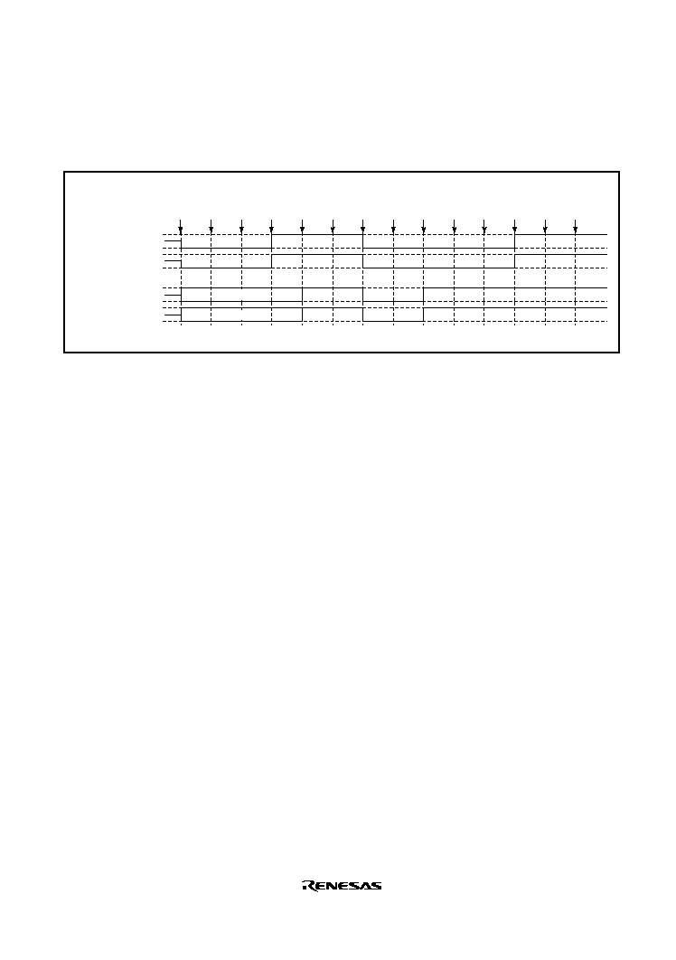
Rev. 2.0, 09/02, page 309 of 732
Operation when Error Occurs during Normal Mode Operation, and Operation is Restarted
in Normal Mode: Figure 11.85 shows an explanatory diagram of the case where an error occurs
in normal mode and operation is restarted in normal mode after re-setting.
1
RESET
2
TMDR
(normal)
3
TOER
(1)
5
PFC
(MTU)
4
TIOR
(1 init
0 out)
6
TSTR
(1)
7
Match
8
Error
occurs
9
PFC
(PORT)
10
TSTR
(0)
11
TMDR
(normal)
12
TIOR
(1 init
0 out)
13
PFC
(MTU)
14
TSTR
(1)
MTU module output
TIOC
*
A
TIOC
*
B
Port output
PEn
PEn
n=0 to 15
High-Z
High-Z
Figure 11.85 Error Occurrence in Normal Mode, Recovery in Normal Mode
1.
After a reset, MTU output is low and ports are in the high-impedance state.
2.
After a reset, the TMDR setting is for normal mode.
3.
For channels 3 and 4, enable output with TOER before initializing the pins with TIOR.
4.
Initialize the pins with TIOR. (The example shows initial high output, with low output on
compare-match occurrence.)
5.
Set MTU output with the PFC.
6.
The count operation is started by TSTR.
7.
Output goes low on compare-match occurrence.
8.
An error occurs.
9.
Set port output with the PFC and output the inverse of the active level.
10. Not necessary when restarting in normal mode.
11. The count operation is stopped by TSTR.
12. Initialize the pins with TIOR.
13. Set MTU output with the PFC.
14. Operation is restarted by TSTR.

Rev. 2.0, 09/02, page 310 of 732
Operation when Error Occurs during Normal Mode Operation, and Operation is Restarted
in PWM Mode 1: Figure 11.86 shows an explanatory diagram of the case where an error occurs
in normal mode and operation is restarted in PWM mode 1 after re-setting.
1
RESET
2
TMDR
(normal)
3
TOER
(1)
5
PFC
(MTU)
4
TIOR
(1 init
0 out)
6
TSTR
(1)
7
Match
8
Error
occurs
9
PFC
(PORT)
10
TSTR
(0)
11
TMDR
(PWM1)
12
TIOR
(1 init
0 out)
13
PFC
(MTU)
14
TSTR
(1)
MTU module output
TIOC
*
A
TIOC
*
B
Port output
PEn
PEn
Not initialized (TIOC
*
B)
n=0 to 15
High-Z
High-Z
Figure 11.86 Error Occurrence in Normal Mode, Recovery in PWM Mode 1
1 to 10 are the same as in figure 11.85.
11. Set PWM mode 1.
12. Initialize the pins with TIOR. (In PWM mode 1, the TIOC*B side is not initialized. If
initialization is required, initialize in normal mode, then switch to PWM mode 1.)
13. Set MTU output with the PFC.
14. Operation is restarted by TSTR.
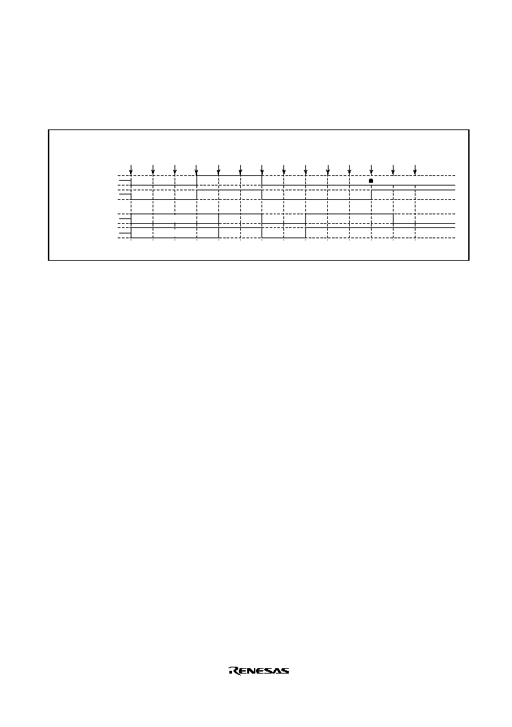
Rev. 2.0, 09/02, page 311 of 732
Operation when Error Occurs during Normal Mode Operation, and Operation is Restarted
in PWM Mode 2: Figure 11.87 shows an explanatory diagram of the case where an error occurs
in normal mode and operation is restarted in PWM mode 2 after re-setting.
1
RESET
2
TMDR
(normal)
3
TOER
(1)
5
PFC
(MTU)
4
TIOR
(1 init
0 out)
6
TSTR
(1)
7
Match
8
Error
occurs
9
PFC
(PORT)
10
TSTR
(0)
11
TMDR
(PWM2)
12
TIOR
(1 init
0 out)
13
PFC
(MTU)
14
TSTR
(1)
MTU module output
TIOC
*
A
TIOC
*
B
Port output
PEn
PEn
Not initialized (cycle register)
n=0 to 15
High-Z
High-Z
Figure 11.87 Error Occurrence in Normal Mode, Recovery in PWM Mode 2
1 to 10 are the same as in figure 11.85.
11. Set PWM mode 2.
12. Initialize the pins with TIOR. (In PWM mode 2, the cycle register pins are not initialized. If
initialization is required, initialize in normal mode, then switch to PWM mode 2.)
13. Set MTU output with the PFC.
14. Operation is restarted by TSTR.
Note:
PWM mode 2 can only be set for channels 0 to 2, and therefore TOER setting is not
necessary.
Rev. 2.0, 09/02, page 312 of 732
Operation when Error Occurs during Normal Mode Operation, and Operation is Restarted
in Phase Counting Mode: Figure 11.88 shows an explanatory diagram of the case where an error
occurs in normal mode and operation is restarted in phase counting mode after re-setting.
1
RESET
2
TMDR
(normal)
3
TOER
(1)
5
PFC
(MTU)
4
TIOR
(1 init
0 out)
6
TSTR
(1)
7
Match
8
Error
occurs
9
PFC
(PORT)
10
TSTR
(0)
11
TMDR
(PCM)
12
TIOR
(1 init
0 out)
13
PFC
(MTU)
14
TSTR
(1)
MTU module output
TIOC
*
A
TIOC
*
B
Port output
PEn
PEn
n=0 to 15
High-Z
High-Z
Figure 11.88 Error Occurrence in Normal Mode, Recovery in Phase Counting Mode
1 to 10 are the same as in figure 11.85.
11. Set phase counting mode.
12. Initialize the pins with TIOR.
13. Set MTU output with the PFC.
14. Operation is restarted by TSTR.
Note:
Phase counting mode can only be set for channels 1 and 2, and therefore TOER setting is
not necessary.
Rev. 2.0, 09/02, page 313 of 732
Operation when Error Occurs during Normal Mode Operation, and Operation is Restarted
in Complementary PWM Mode: Figure 11.89 shows an explanatory diagram of the case where
an error occurs in normal mode and operation is restarted in complementary PWM mode after re-
setting.
1
RESET
2
TMDR
(normal)
3
TOER
(1)
5
PFC
(MTU)
4
TIOR
(1 init
0 out)
6
TSTR
(1)
7
Match
8
Error
occurs
9
PFC
(PORT)
10
TSTR
(0)
11
TIOR
(0 init
0 out)
12
TIOR
(disabled)
13
TOER
(0)
14
TOCR
15
TMDR
(CPWM)
(16)
TOER
(1)
(17)
PFC
(MTU)
(18)
TSTR
(1)
MTU
module
output
TIOC3A
TIOC3B
TIOC3D
Port output
PE9
PE8
PE11
High-Z
High-Z
High-Z
Figure 11.89 Error Occurrence in Normal Mode, Recovery in Complementary PWM Mode
1 to 10 are the same as in figure 11.85.
11. Initialize the normal mode waveform generation section with TIOR.
12. Disable operation of the normal mode waveform generation section with TIOR.
13. Disable channel 3 and 4 output with TOER.
14. Select the complementary PWM output level and cyclic output enabling/disabling with
TOCR.
15. Set complementary PWM.
16. Enable channel 3 and 4 output with TOER.
17. Set MTU output with the PFC.
18. Operation is restarted by TSTR.
Rev. 2.0, 09/02, page 314 of 732
Operation when Error Occurs during Normal Mode Operation, and Operation is Restarted
in Reset-Synchronous PWM Mode: Figure 11.90 shows an explanatory diagram of the case
where an error occurs in normal mode and operation is restarted in reset-synchronous PWM mode
after re-setting.
1
RESET
2
TMDR
(normal)
3
TOER
(1)
5
PFC
(MTU)
4
TIOR
(1 init
0 out)
6
TSTR
(1)
7
Match
8
Error
occurs
9
PFC
(PORT)
10
TSTR
(0)
11
TIOR
(0 init
0 out)
12
TIOR
(disabled)
13
TOER
(0)
14
TOCR
15
TMDR
(CPWM)
16
TOER
(1)
17
PFC
(MTU)
18
TSTR
(1)
MTU
module
output
TIOC3A
TIOC3B
TIOC3D
Port output
PE9
PE8
PE11
High-Z
High-Z
High-Z
Figure 11.90 Error Occurrence in Normal Mode,
Recovery in Reset-Synchronous PWM Mode
1 to 13 are the same as in figure 11.89.
14. Select the reset-synchronous PWM output level and cyclic output enabling/disabling with
TOCR.
15. Set reset-synchronous PWM.
16. Enable channel 3 and 4 output with TOER.
17. Set MTU output with the PFC.
18. Operation is restarted by TSTR.
Rev. 2.0, 09/02, page 315 of 732
Operation when Error Occurs during PWM Mode 1 Operation, and Operation is Restarted
in Normal Mode: Figure 11.91 shows an explanatory diagram of the case where an error occurs
in PWM mode 1 and operation is restarted in normal mode after re-setting.
1
RESET
2
TMDR
(PWM1)
3
TOER
(1)
5
PFC
(MTU)
4
TIOR
(1 init
0 out)
6
TSTR
(1)
7
Match
8
Error
occurs
9
PFC
(PORT)
10
TSTR
(0)
11
TMDR
(normal)
12
TIOR
(1 init
0 out)
13
PFC
(MTU)
14
TSTR
(1)
MTU module output
TIOC
*
A
TIOC
*
B
Port output
PEn
PEn
Not initialized (TIOC
*
B)
n=0 to 15
High-Z
High-Z
Figure 11.91 Error Occurrence in PWM Mode 1, Recovery in Normal Mode
1.
After a reset, MTU output is low and ports are in the high-impedance state.
2.
Set PWM mode 1.
3.
For channels 3 and 4, enable output with TOER before initializing the pins with TIOR.
4.
Initialize the pins with TIOR. (The example shows initial high output, with low output on
compare-match occurrence. In PWM mode 1, the TIOC*B side is not initialized.)
5.
Set MTU output with the PFC.
6.
The count operation is started by TSTR.
7.
Output goes low on compare-match occurrence.
8.
An error occurs.
9.
Set port output with the PFC and output the inverse of the active level.
10. The count operation is stopped by TSTR.
11. Set normal mode.
12. Initialize the pins with TIOR.
13. Set MTU output with the PFC.
14. Operation is restarted by TSTR.
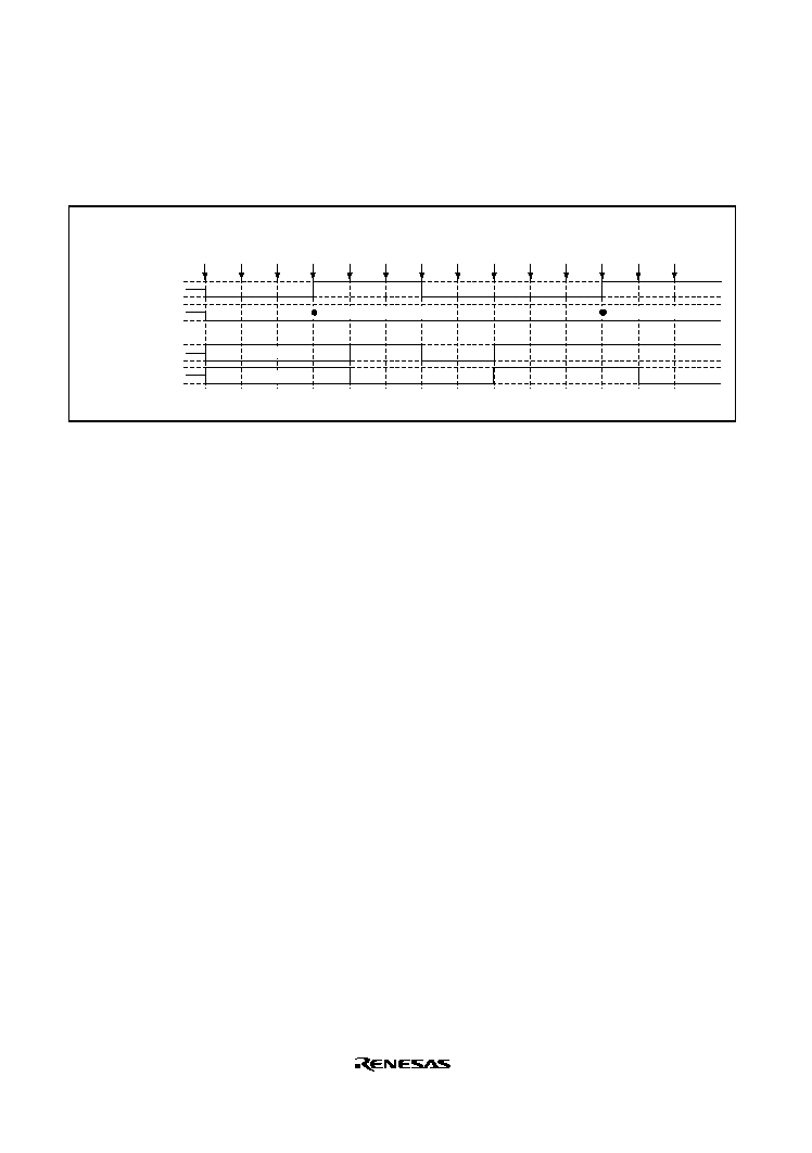
Rev. 2.0, 09/02, page 316 of 732
Operation when Error Occurs during PWM Mode 1 Operation, and Operation is Restarted
in PWM Mode 1: Figure 11.92 shows an explanatory diagram of the case where an error occurs
in PWM mode 1 and operation is restarted in PWM mode 1 after re-setting.
1
RESET
2
TMDR
(PWM1)
3
TOER
(1)
5
PFC
(MTU)
4
TIOR
(1 init
0 out)
6
TSTR
(1)
7
Match
8
Error
occurs
9
PFC
(PORT)
10
TSTR
(0)
11
TMDR
(PWM1)
12
TIOR
(1 init
0 out)
13
PFC
(MTU)
14
TSTR
(1)
MTU module output
TIOC
*
A
TIOC
*
B
Port output
PEn
PEn
Not initialized (TIOC
*
B)
Not initialized (TIOC
*
B)
n=0 to 15
High-Z
High-Z
Figure 11.92 Error Occurrence in PWM Mode 1, Recovery in PWM Mode 1
1 to 10 are the same as in figure 11.91.
11. Not necessary when restarting in PWM mode 1.
12. Initialize the pins with TIOR. (In PWM mode 1, the TIOC*B side is not initialized.)
13. Set MTU output with the PFC.
14. Operation is restarted by TSTR.
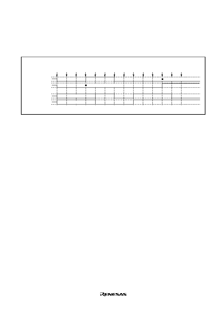
Rev. 2.0, 09/02, page 317 of 732
Operation when Error Occurs during PWM Mode 1 Operation, and Operation is Restarted
in PWM Mode 2: Figure 11.93 shows an explanatory diagram of the case where an error occurs
in PWM mode 1 and operation is restarted in PWM mode 2 after re-setting.
1
RESET
2
TMDR
(PWM1)
3
TOER
(1)
5
PFC
(MTU)
4
TIOR
(1 init
0 out)
6
TSTR
(1)
7
Match
8
Error
occurs
9
PFC
(PORT)
10
TSTR
(0)
11
TMDR
(PWM2)
12
TIOR
(1 init
0 out)
13
PFC
(MTU)
14
TSTR
(1)
MTU module output
TIOC
*
A
TIOC
*
B
Port output
PEn
PEn
Not initialized (TIOC
*
B)
Not initialized (cycle register)
n=0 to 15
High-Z
High-Z
Figure 11.93 Error Occurrence in PWM Mode 1, Recovery in PWM Mode 2
1 to 10 are the same as in figure 11.91.
11. Set PWM mode 2.
12. Initialize the pins with TIOR. (In PWM mode 2, the cycle register pins are not initialized.)
13. Set MTU output with the PFC.
14. Operation is restarted by TSTR.
Note:
PWM mode 2 can only be set for channels 0 to 2, and therefore TOER setting is not
necessary.

Rev. 2.0, 09/02, page 318 of 732
Operation when Error Occurs during PWM Mode 1 Operation, and Operation is Restarted
in Phase Counting Mode: Figure 11.94 shows an explanatory diagram of the case where an error
occurs in PWM mode 1 and operation is restarted in phase counting mode after re-setting.
1
RESET
2
TMDR
(PWM1)
3
TOER
(1)
5
PFC
(MTU)
4
TIOR
(1 init
0 out)
6
TSTR
(1)
7
Match
8
Error
occurs
9
PFC
(PORT)
10
TSTR
(0)
11
TMDR
(PCM)
12
TIOR
(1 init
0 out)
13
PFC
(MTU)
14
TSTR
(1)
MTU module output
TIOC
*
A
TIOC
*
B
Port output
PEn
PEn
Not initialized (TIOC
*
B)
n=0 to 15
High-Z
High-Z
Figure 11.94 Error Occurrence in PWM Mode 1, Recovery in Phase Counting Mode
1 to 10 are the same as in figure 11.91.
11. Set phase counting mode.
12. Initialize the pins with TIOR.
13. Set MTU output with the PFC.
14. Operation is restarted by TSTR.
Note:
Phase counting mode can only be set for channels 1 and 2, and therefore TOER setting is
not necessary.
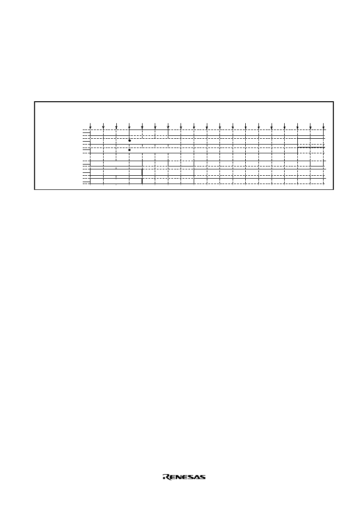
Rev. 2.0, 09/02, page 319 of 732
Operation when Error Occurs during PWM Mode 1 Operation, and Operation is Restarted
in Complementary PWM Mode: Figure 11.95 shows an explanatory diagram of the case where
an error occurs in PWM mode 1 and operation is restarted in complementary PWM mode after re-
setting.
1
RESET
2
TMDR
(PWM1)
3
TOER
(1)
5
PFC
(MTU)
4
TIOR
(1 init
0 out)
6
TSTR
(1)
7
Match
8
Error
occurs
9
PFC
(PORT)
10
TSTR
(0)
11
TMDR
(normal)
12
TIOR
(0 init
0 out)
13
TIOR
(disabled)
14
TOER
(0)
15
TOCR
16
TMDR
(CPWM)
17
TOER
(1)
18
PFC
(MTU)
19
TSTR
(1)
MTU
module
output
TIOC3A
TIOC3B
TIOC3D
Port output
PE9
PE8
PE11
Not initialized (TIOC3B)
Not initialized (TIOC3D)
High-Z
High-Z
High-Z
Figure 11.95 Error Occurrence in PWM Mode 1,
Recovery in Complementary PWM Mode
1 to 10 are the same as in figure 11.91.
11. Set normal mode for initialization of the normal mode waveform generation section.
12. Initialize the PWM mode 1 waveform generation section with TIOR.
13. Disable operation of the PWM mode 1 waveform generation section with TIOR.
14. Disable channel 3 and 4 output with TOER.
15. Select the complementary PWM output level and cyclic output enabling/disabling with
TOCR.
16. Set complementary PWM.
17. Enable channel 3 and 4 output with TOER.
18. Set MTU output with the PFC.
19. Operation is restarted by TSTR.
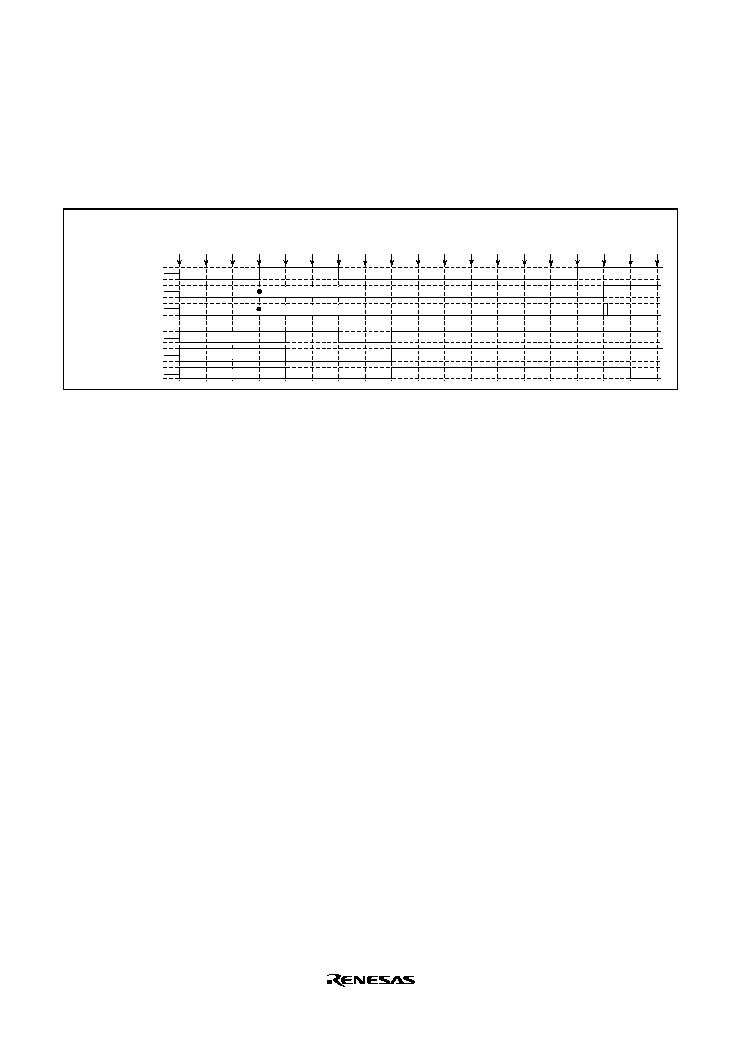
Rev. 2.0, 09/02, page 320 of 732
Operation when Error Occurs during PWM Mode 1 Operation, and Operation is Restarted
in Reset-Synchronous PWM Mode: Figure 11.96 shows an explanatory diagram of the case
where an error occurs in PWM mode 1 and operation is restarted in reset-synchronous PWM mode
after re-setting.
1
RESET
2
TMDR
(PWM1)
3
TOER
(1)
5
PFC
(MTU)
4
TIOR
(1 init
0 out)
6
TSTR
(1)
7
Match
8
Error
occurs
9
PFC
(PORT)
10
TSTR
(0)
11
TMDR
(normal)
12
TIOR
(0 init
0 out)
13
TIOR
(disabled)
14
TOER
(0)
15
TOCR
16
TMDR
(RPWM)
17
TOER
(1)
18
PFC
(MTU)
19
TSTR
(1)
MTU
module
output
TIOC3A
TIOC3B
TIOC3D
Port output
PE9
PE8
PE11
Not initialized (TIOC3B)
Not initialized (TIOC3D)
High-Z
High-Z
High-Z
Figure 11.96 Error Occurrence in PWM Mode 1,
Recovery in Reset-Synchronous PWM Mode
1 to 14 are the same as in figure 11.95.
15. Select the reset-synchronous PWM output level and cyclic output enabling/disabling with
TOCR.
16. Set reset-synchronous PWM.
17. Enable channel 3 and 4 output with TOER.
18. Set MTU output with the PFC.
19. Operation is restarted by TSTR.
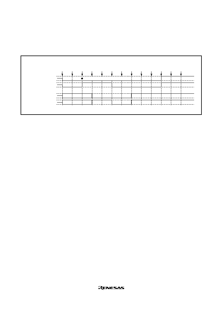
Rev. 2.0, 09/02, page 321 of 732
Operation when Error Occurs during PWM Mode 2 Operation, and Operation is Restarted
in Normal Mode: Figure 11.97 shows an explanatory diagram of the case where an error occurs
in PWM mode 2 and operation is restarted in normal mode after re-setting.
1
RESET
2
TMDR
(PWM2)
3
TIOR
(1 init
0 out)
5
TSTR
(1)
4
PFC
(MTU)
6
Match
7
Error
occurs
8
PFC
(PORT)
9
TSTR
(0)
10
TMDR
(normal)
11
TIOR
(1 init
0 out)
12
PFC
(MTU)
13
TSTR
(1)
MTU module output
TIOC
*
A
TIOC
*
B
Port output
PEn
PEn
Not initialized (cycle register)
n=0 to 15
High-Z
High-Z
Figure 11.97 Error Occurrence in PWM Mode 2, Recovery in Normal Mode
1.
After a reset, MTU output is low and ports are in the high-impedance state.
2.
Set PWM mode 2.
3.
Initialize the pins with TIOR. (The example shows initial high output, with low output on
compare-match occurrence. In PWM mode 2, the cycle register pins are not initialized. In the
example, TIOC *A is the cycle register.)
4.
Set MTU output with the PFC.
5.
The count operation is started by TSTR.
6.
Output goes low on compare-match occurrence.
7.
An error occurs.
8.
Set port output with the PFC and output the inverse of the active level.
9.
The count operation is stopped by TSTR.
10. Set normal mode.
11. Initialize the pins with TIOR.
12.
Set MTU output with the PFC.
13.
Operation is restarted by TSTR.
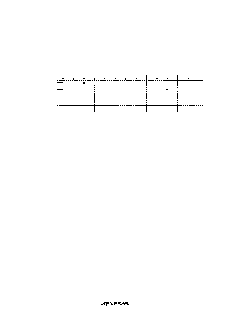
Rev. 2.0, 09/02, page 322 of 732
Operation when Error Occurs during PWM Mode 2 Operation, and Operation is Restarted
in PWM Mode 1: Figure 11.98 shows an explanatory diagram of the case where an error occurs
in PWM mode 2 and operation is restarted in PWM mode 1 after re-setting.
1
RESET
2
TMDR
(PWM2)
3
TIOR
(1 init
0 out)
5
TSTR
(1)
4
PFC
(MTU)
6
Match
7
Error
occurs
8
PFC
(PORT)
9
TSTR
(0)
10
TMDR
(PWM1)
11
TIOR
(1 init
0 out)
12
PFC
(MTU)
13
TSTR
(1)
MTU module output
TIOC
*
A
TIOC
*
B
Port output
PEn
PEn
Not initialized (TIOC
*
B)
Not initialized (cycle register)
n=0 to 15
High-Z
High-Z
Figure 11.98 Error Occurrence in PWM Mode 2, Recovery in PWM Mode 1
1 to 9 are the same as in figure 11.97.
10. Set PWM mode 1.
11. Initialize the pins with TIOR. (In PWM mode 1, the TIOC*B side is not initialized.)
12. Set MTU output with the PFC.
13. Operation is restarted by TSTR.
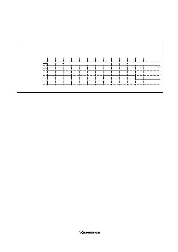
Rev. 2.0, 09/02, page 323 of 732
Operation when Error Occurs during PWM Mode 2 Operation, and Operation is Restarted
in PWM Mode 2: Figure 11.99 shows an explanatory diagram of the case where an error occurs
in PWM mode 2 and operation is restarted in PWM mode 2 after re-setting.
1
RESET
2
TMDR
(PWM2)
3
TIOR
(1 init
0 out)
5
TSTR
(1)
4
PFC
(MTU)
6
Match
7
Error
occurs
8
PFC
(PORT)
9
TSTR
(0)
10
TMDR
(PWM2)
11
TIOR
(1 init
0 out)
12
PFC
(MTU)
13
TSTR
(1)
MTU module output
TIOC
*
A
TIOC
*
B
Port output
PEn
PEn
Not initialized (cycle register)
Not initialized (cycle register)
n=0 to 15
High-Z
High-Z
Figure 11.99 Error Occurrence in PWM Mode 2, Recovery in PWM Mode 2
1 to 9 are the same as in figure 11.97.
10. Not necessary when restarting in PWM mode 2.
11. Initialize the pins with TIOR. (In PWM mode 2, the cycle register pins are not initialized.)
12. Set MTU output with the PFC.
13. Operation is restarted by TSTR.
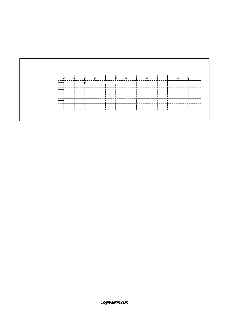
Rev. 2.0, 09/02, page 324 of 732
Operation when Error Occurs during PWM Mode 2 Operation, and Operation is Restarted
in Phase Counting Mode: Figure 11.100 shows an explanatory diagram of the case where an
error occurs in PWM mode 2 and operation is restarted in phase counting mode after re-setting.
1
RESET
2
TMDR
(PWM2)
3
TIOR
(1 init
0 out)
5
TSTR
(1)
4
PFC
(MTU)
6
Match
7
Error
occurs
8
PFC
(PORT)
9
TSTR
(0)
10
TMDR
(PCM)
11
TIOR
(1 init
0 out)
12
PFC
(MTU)
13
TSTR
(1)
MTU module output
TIOC
*
A
TIOC
*
B
Port output
PEn
PEn
Not initialized (cycle register)
n=0 to 15
High-Z
High-Z
Figure 11.100 Error Occurrence in PWM Mode 2, Recovery in Phase Counting Mode
1 to 9 are the same as in figure 11.97.
10. Set phase counting mode.
11. Initialize the pins with TIOR.
12. Set MTU output with the PFC.
13. Operation is restarted by TSTR.
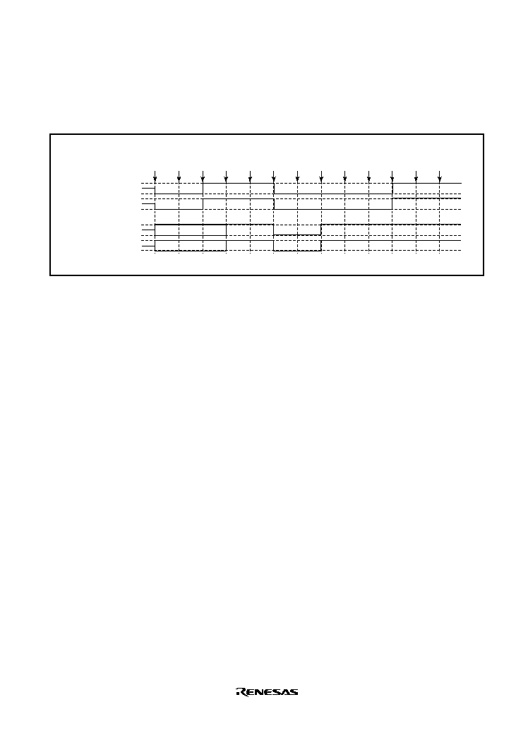
Rev. 2.0, 09/02, page 325 of 732
Operation when Error Occurs during Phase Counting Mode Operation, and Operation is
Restarted in Normal Mode: Figure 11.101 shows an explanatory diagram of the case where an
error occurs in phase counting mode and operation is restarted in normal mode after re-setting.
1
RESET
2
TMDR
(PCM)
3
TIOR
(1 init
0 out)
5
TSTR
(1)
4
PFC
(MTU)
6
Match
7
Error
occurs
8
PFC
(PORT)
9
TSTR
(0)
10
TMDR
(normal)
11
TIOR
(1 init
0 out)
12
PFC
(MTU)
13
TSTR
(1)
MTU module output
TIOC
*
A
TIOC
*
B
Port output
PEn
PEn
n=0 to 15
High-Z
High-Z
Figure 11.101 Error Occurrence in Phase Counting Mode, Recovery in Normal Mode
1.
After a reset, MTU output is low and ports are in the high-impedance state.
2.
Set phase counting mode.
3.
Initialize the pins with TIOR. (The example shows initial high output, with low output on
compare-match occurrence.)
4.
Set MTU output with the PFC.
5.
The count operation is started by TSTR.
6.
Output goes low on compare-match occurrence.
7.
An error occurs.
8.
Set port output with the PFC and output the inverse of the active level.
9.
The count operation is stopped by TSTR.
10. Set in normal mode.
11. Initialize the pins with TIOR.
12. Set MTU output with the PFC.
13. Operation is restarted by TSTR.
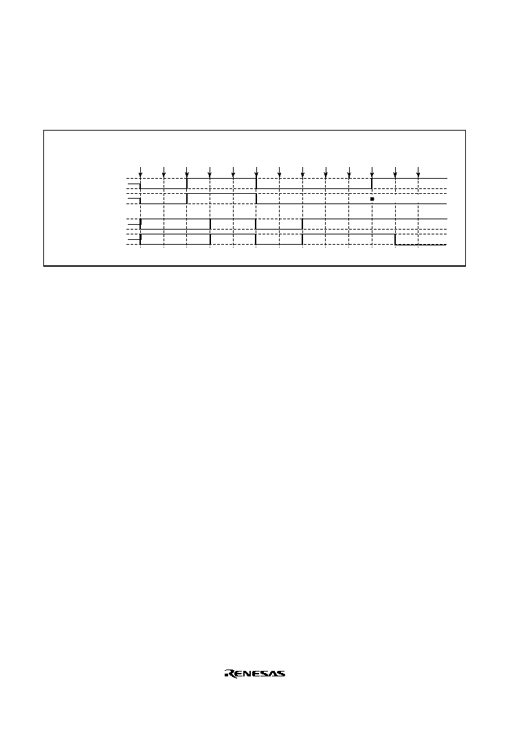
Rev. 2.0, 09/02, page 326 of 732
Operation when Error Occurs during Phase Counting Mode Operation, and Operation is
Restarted in PWM Mode 1: Figure 11.102 shows an explanatory diagram of the case where an
error occurs in phase counting mode and operation is restarted in PWM mode 1 after re-setting.
1
RESET
2
TMDR
(PCM)
3
TIOR
(1 init
0 out)
5
TSTR
(1)
4
PFC
(MTU)
6
Match
7
Error
occurs
8
PFC
(PORT)
9
TSTR
(0)
10
TMDR
(PWM1)
11
TIOR
(1 init
0 out)
12
PFC
(MTU)
13
TSTR
(1)
MTU module output
TIOC
*
A
TIOC
*
B
Port output
PEn
PEn
Not initialized (TIOC
*
B)
n=0 to 15
High-Z
High-Z
Figure 11.102 Error Occurrence in Phase Counting Mode, Recovery in PWM Mode 1
1 to 9 are the same as in figure 11.101.
10. Set PWM mode 1.
11. Initialize the pins with TIOR. (In PWM mode 1, the TIOC *B side is not initialized.)
12. Set MTU output with the PFC.
13. Operation is restarted by TSTR.

Rev. 2.0, 09/02, page 327 of 732
Operation when Error Occurs during Phase Counting Mode Operation, and Operation is
Restarted in PWM Mode 2: Figure 11.103 shows an explanatory diagram of the case where an
error occurs in phase counting mode and operation is restarted in PWM mode 2 after re-setting.
1
RESET
2
TMDR
(PCM)
3
TIOR
(1 init
0 out)
5
TSTR
(1)
4
PFC
(MTU)
6
Match
7
Error
occurs
8
PFC
(PORT)
9
TSTR
(0)
10
TMDR
(PWM2)
11
TIOR
(1 init
0 out)
12
PFC
(MTU)
13
TSTR
(1)
MTU module output
TIOC
*
A
TIOC
*
B
Port output
PEn
PEn
n=0 to 15
High-Z
High-Z
Not initialized (cycle register)
Figure 11.103 Error Occurrence in Phase Counting Mode, Recovery in PWM Mode 2
1 to 9 are the same as in figure 11.101.
10. Set PWM mode 2.
11. Initialize the pins with TIOR. (In PWM mode 2, the cycle register pins are not initialized.)
12. Set MTU output with the PFC.
13. Operation is restarted by TSTR.

Rev. 2.0, 09/02, page 328 of 732
Operation when Error Occurs during Phase Counting Mode Operation, and Operation is
Restarted in Phase Counting Mode: Figure 11.104 shows an explanatory diagram of the case
where an error occurs in phase counting mode and operation is restarted in phase counting mode
after re-setting.
1
RESET
2
TMDR
(PCM)
3
TIOR
(1 init
0 out)
5
TSTR
(1)
4
PFC
(MTU)
6
Match
7
Error
occurs
8
PFC
(PORT)
9
TSTR
(0)
10
TMDR
(PCM)
11
TIOR
(1 init
0 out)
12
PFC
(MTU)
13
TSTR
(1)
MTU module output
TIOC
*
A
TIOC
*
B
Port output
PEn
PEn
n=0 to 15
High-Z
High-Z
Figure 11.104 Error Occurrence in Phase Counting Mode,
Recovery in Phase Counting Mode
1 to 9 are the same as in figure 11.101.
10. Not necessary when restarting in phase counting mode.
11. Initialize the pins with TIOR.
12. Set MTU output with the PFC.
13. Operation is restarted by TSTR.
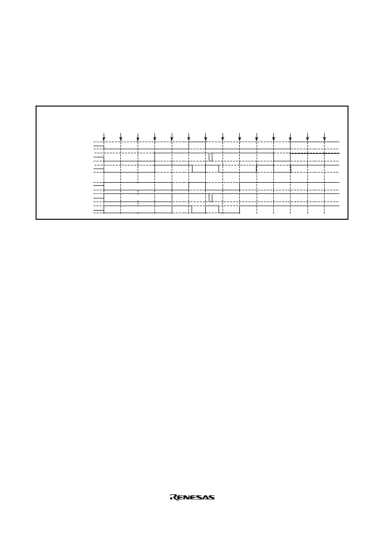
Rev. 2.0, 09/02, page 329 of 732
Operation when Error Occurs during Complementary PWM Mode Operation, and
Operation is Restarted in Normal Mode: Figure 11.105 shows an explanatory diagram of the
case where an error occurs in complementary PWM mode and operation is restarted in normal
mode after re-setting.
1
RESET
2
TOCR
3
TMDR
(CPWM)
5
PFC
(MTU)
4
TOER
(1)
6
TSTR
(1)
7
Match
8
Error
occurs
9
PFC
(PORT)
10
TSTR
(0)
11
TMDR
(normal)
12
TIOR
(1 init
0 out)
13
PFC
(MTU)
14
TSTR
(1)
MTU module output
TIOC3A
TIOC3B
TIOC3D
Port output
PE9
PE8
PE11
High-Z
High-Z
High-Z
Figure 11.105 Error Occurrence in Complementary PWM Mode,
Recovery in Normal Mode
1.
After a reset, MTU output is low and ports are in the high-impedance state.
2.
Select the complementary PWM output level and cyclic output enabling/disabling with
TOCR.
3.
Set complementary PWM.
4.
Enable channel 3 and 4 output with TOER.
5.
Set MTU output with the PFC.
6.
The count operation is started by TSTR.
7.
The complementary PWM waveform is output on compare-match occurrence.
8.
An error occurs.
9.
Set port output with the PFC and output the inverse of the active level.
10. The count operation is stopped by TSTR. (MTU output becomes the complementary PWM
output initial value.)
11. Set normal mode. (MTU output goes low.)
12. Initialize the pins with TIOR.
13. Set MTU output with the PFC.
14. Operation is restarted by TSTR.

Rev. 2.0, 09/02, page 330 of 732
Operation when Error Occurs during Complementary PWM Mode Operation, and
Operation is Restarted in PWM Mode 1: Figure 11.106 shows an explanatory diagram of the
case where an error occurs in complementary PWM mode and operation is restarted in PWM
mode 1 after re-setting.
1
RESET
2
TOCR
3
TMDR
(CPWM)
5
PFC
(MTU)
4
TOER
(1)
6
TSTR
(1)
7
Match
8
Error
occurs
9
PFC
(PORT)
10
TSTR
(0)
11
TMDR
(PWM1)
12
TIOR
(1 init
0 out)
13
PFC
(MTU)
14
TSTR
(1)
MTU module output
TIOC3A
TIOC3B
TIOC3D
Port output
PE9
PE8
PE11
Not initialized (TIOC3B)
Not initialized (TIOC3D)
High-Z
High-Z
High-Z
Figure 11.106 Error Occurrence in Complementary PWM Mode,
Recovery in PWM Mode 1
1 to 10 are the same as in figure 11.105.
11. Set PWM mode 1. (MTU output goes low.)
12. Initialize the pins with TIOR. (In PWM mode 1, the TIOC *B side is not initialized.)
13. Set MTU output with the PFC.
14. Operation is restarted by TSTR.
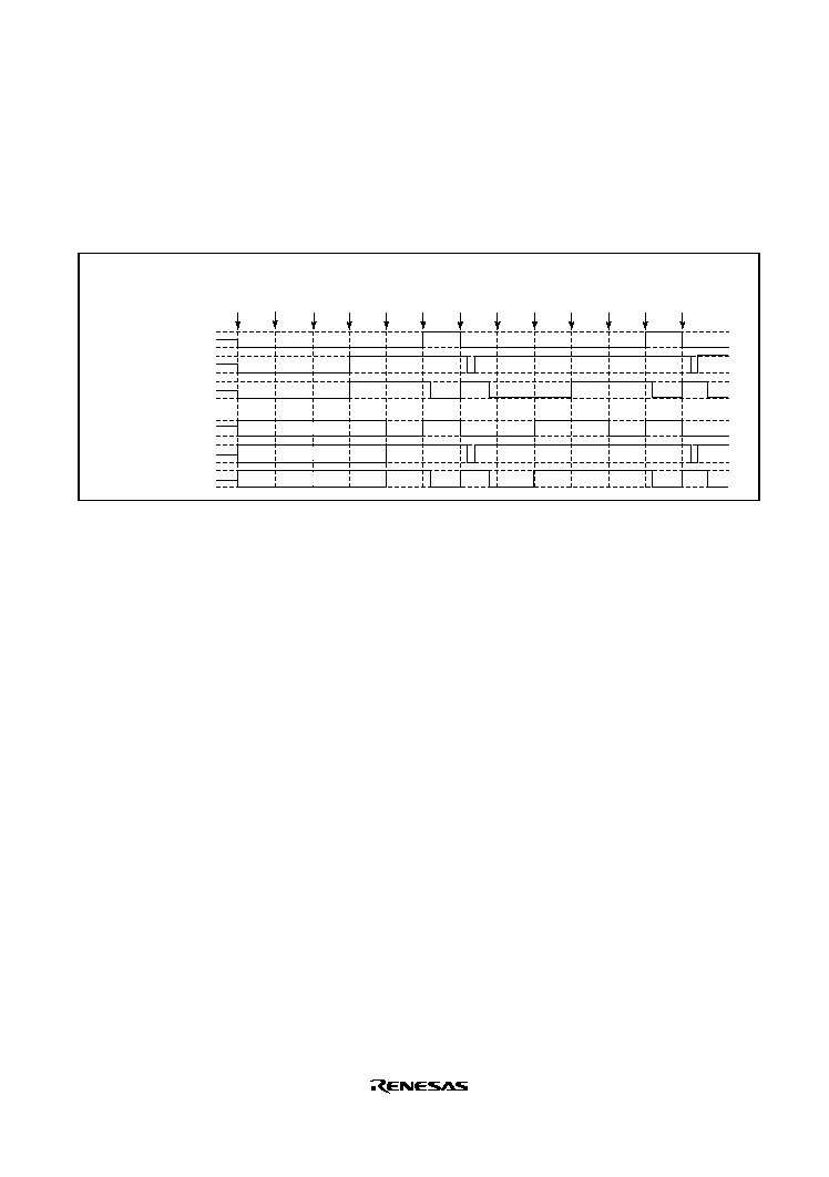
Rev. 2.0, 09/02, page 331 of 732
Operation when Error Occurs during Complementary PWM Mode Operation, and
Operation is Restarted in Complementary PWM Mode: Figure 11.107 shows an explanatory
diagram of the case where an error occurs in complementary PWM mode and operation is
restarted in complementary PWM mode after re-setting (when operation is restarted using the
cycle and duty settings at the time the counter was stopped).
1
RESET
2
TOCR
3
TMDR
(CPWM)
5
PFC
(MTU)
4
TOER
(1)
6
TSTR
(1)
7
Match
8
Error
occurs
9
PFC
(PORT)
10
TSTR
(0)
11
PFC
(MTU)
12
TSTR
(1)
13
Match
MTU module output
TIOC3A
TIOC3B
TIOC3D
Port output
PE9
PE8
PE11
High-Z
High-Z
High-Z
Figure 11.107 Error Occurrence in Complementary PWM Mode,
Recovery in Complementary PWM Mode
1 to 10 are the same as in figure 11.105.
11. Set MTU output with the PFC.
12. Operation is restarted by TSTR.
13. The complementary PWM waveform is output on compare-match occurrence.
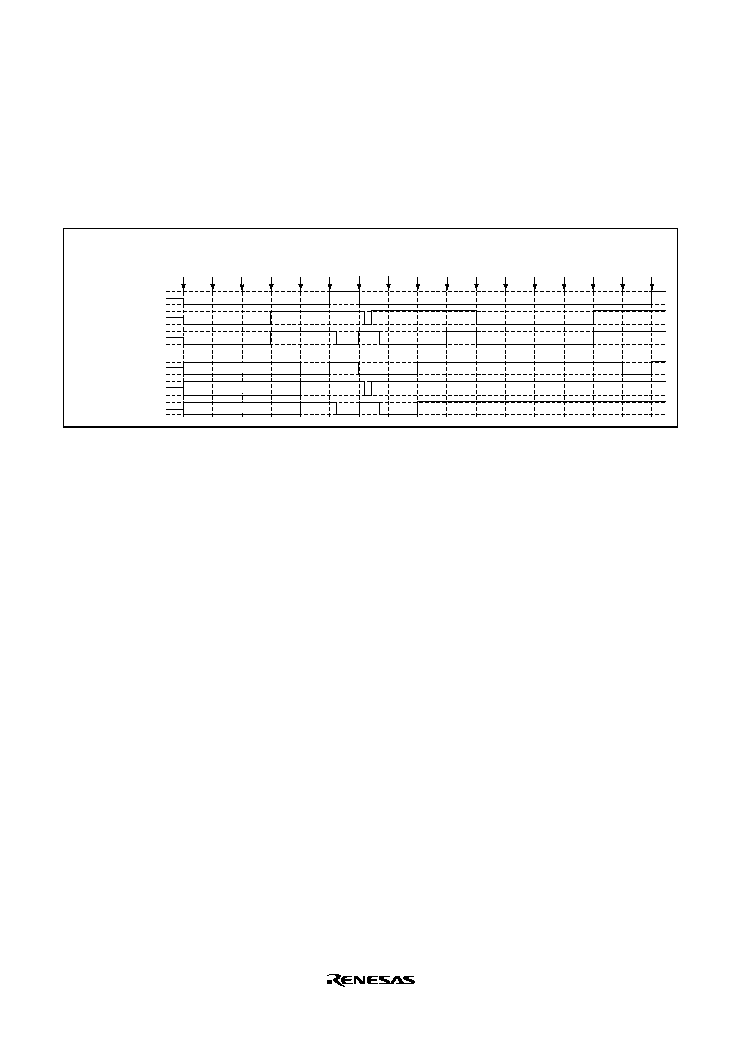
Rev. 2.0, 09/02, page 332 of 732
Operation when Error Occurs during Complementary PWM Mode Operation, and
Operation is Restarted in Complementary PWM Mode: Figure 11.108 shows an explanatory
diagram of the case where an error occurs in complementary PWM mode and operation is
restarted in complementary PWM mode after re-setting (when operation is restarted using
completely new cycle and duty settings).
1
RESET
2
TOCR
3
TMDR
(CPWM)
5
PFC
(MTU)
4
TOER
(1)
6
TSTR
(1)
7
Match
8
Error
occurs
9
PFC
(PORT)
10
TSTR
(0)
11
TMDR
(normal)
12
TOER
(0)
13
TOCR
14
TMDR
(CPWM)
15
TOER
(1)
16
PFC
(MTU)
17
TSTR
(1)
MTU
module
output
TIOC3A
TIOC3B
TIOC3D
Port output
PE9
PE8
PE11
High-Z
High-Z
High-Z
Figure 11.108 Error Occurrence in Complementary PWM Mode,
Recovery in Complementary PWM Mode
1 to 10 are the same as in figure 11.105.
11. Set normal mode and make new settings. (MTU output goes low.)
12. Disable channel 3 and 4 output with TOER.
13. Select the complementary PWM mode output level and cyclic output enabling/disabling with
TOCR.
14. Set complementary PWM.
15. Enable channel 3 and 4 output with TOER.
16. Set MTU output with the PFC.
17. Operation is restarted by TSTR.
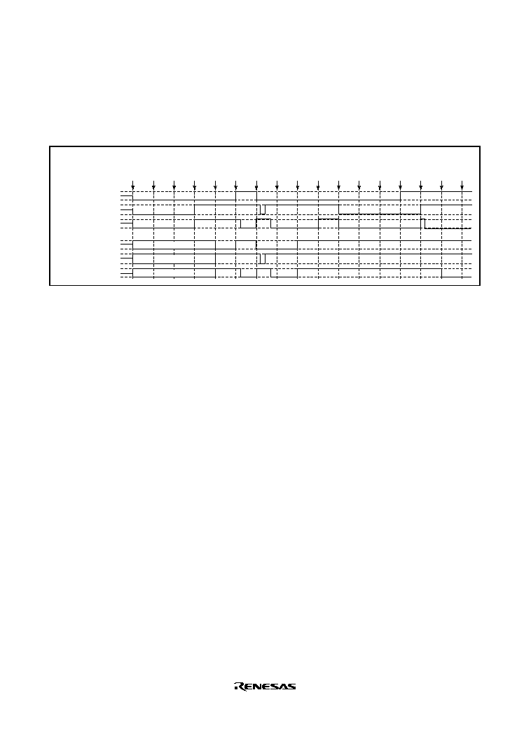
Rev. 2.0, 09/02, page 333 of 732
Operation when Error Occurs during Complementary PWM Mode Operation, and
Operation is Restarted in Reset-Synchronous PWM Mode: Figure 11.109 shows an
explanatory diagram of the case where an error occurs in complementary PWM mode and
operation is restarted in reset-synchronous PWM mode.
1
RESET
2
TOCR
3
TMDR
(CPWM)
5
PFC
(MTU)
4
TOER
(1)
6
TSTR
(1)
7
Match
8
Error
occurs
9
PFC
(PORT)
10
TSTR
(0)
11
TMDR
(normal)
12
TOER
(0)
13
TOCR
14
TMDR
(RPWM)
15
TOER
(1)
16
PFC
(MTU)
17
TSTR
(1)
MTU
module
output
TIOC3A
TIOC3B
TIOC3D
Port output
PE9
PE8
PE11
High-Z
High-Z
High-Z
Figure 11.109 Error Occurrence in Complementary PWM Mode,
Recovery in Reset-Synchronous PWM Mode
1 to 10 are the same as in figure 11.105.
11. Set normal mode. (MTU output goes low.)
12. Disable channel 3 and 4 output with TOER.
13. Select the reset-synchronous PWM mode output level and cyclic output enabling/disabling
with TOCR.
14. Set reset-synchronous PWM.
15. Enable channel 3 and 4 output with TOER.
16. Set MTU output with the PFC.
17. Operation is restarted by TSTR.
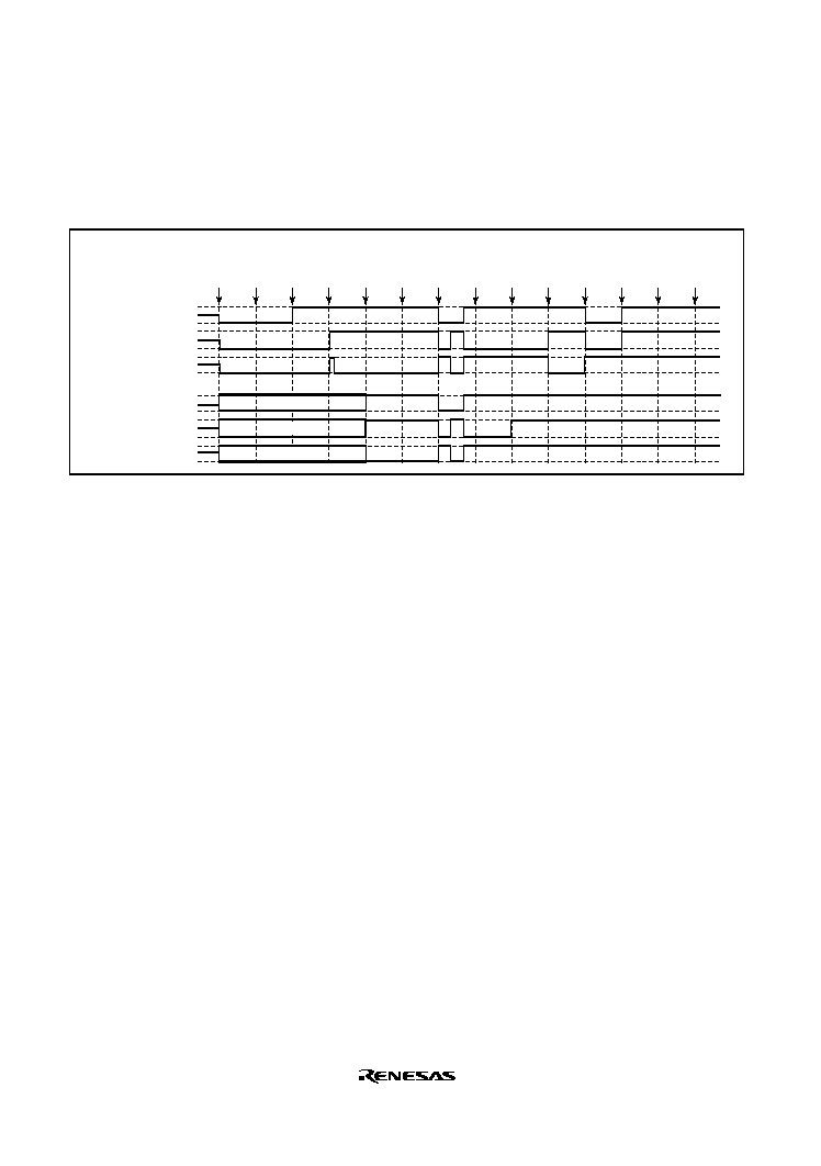
Rev. 2.0, 09/02, page 334 of 732
Operation when Error Occurs during Reset-Synchronous PWM Mode Operation, and
Operation is Restarted in Normal Mode: Figure 11.110 shows an explanatory diagram of the
case where an error occurs in reset-synchronous PWM mode and operation is restarted in normal
mode after re-setting.
1
RESET
2
TOCR
3
TMDR
(CPWM)
5
PFC
(MTU)
4
TOER
(1)
6
TSTR
(1)
7
Match
8
Error
occurs
9
PFC
(PORT)
10
TSTR
(0)
11
TMDR
(normal)
12
TIOR
(1 init
0 out)
13
PFC
(MTU)
14
TSTR
(1)
MTU module output
TIOC3A
TIOC3B
TIOC3D
Port output
PE9
PE8
PE11
High-Z
High-Z
High-Z
Figure 11.110 Error Occurrence in Reset-Synchronous PWM Mode,
Recovery in Normal Mode
1.
After a reset, MTU output is low and ports are in the high-impedance state.
2.
Select the reset-synchronous PWM output level and cyclic output enabling/disabling with
TOCR.
3.
Set reset-synchronous PWM.
4.
Enable channel 3 and 4 output with TOER.
5.
Set MTU output with the PFC.
6.
The count operation is started by TSTR.
7.
The reset-synchronous PWM waveform is output on compare-match occurrence.
8.
An error occurs.
9.
Set port output with the PFC and output the inverse of the active level.
10. The count operation is stopped by TSTR. (MTU output becomes the reset-synchronous PWM
output initial value.)
11. Set normal mode. (MTU positive phase output is low, and negative phase output is high.)
12. Initialize the pins with TIOR.
13. Set MTU output with the PFC.
14. Operation is restarted by TSTR.
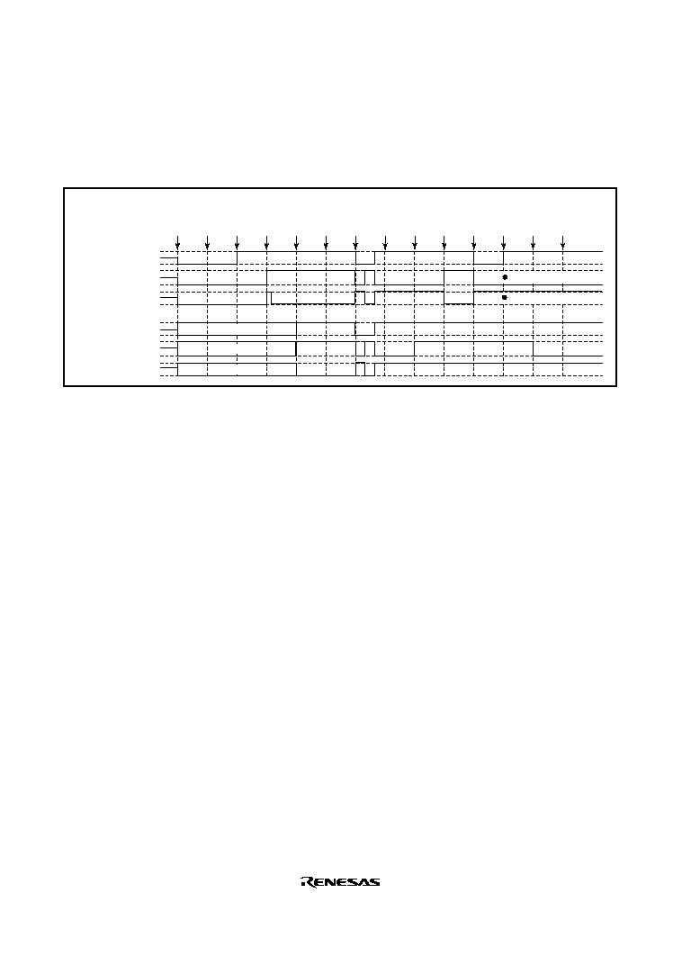
Rev. 2.0, 09/02, page 335 of 732
Operation when Error Occurs during Reset-Synchronous PWM Mode Operation, and
Operation is Restarted in PWM Mode 1: Figure 11.111 shows an explanatory diagram of the
case where an error occurs in reset-synchronous PWM mode and operation is restarted in PWM
mode 1 after re-setting.
1
RESET
2
TOCR
3
TMDR
(RPWM)
5
PFC
(MTU)
4
TOER
(1)
6
TSTR
(1)
7
Match
8
Error
occurs
9
PFC
(PORT)
10
TSTR
(0)
11
TMDR
(PWM1)
12
TIOR
(1 init
0 out)
13
PFC
(MTU)
14
TSTR
(1)
MTU module output
TIOC3A
TIOC3B
TIOC3D
Port output
PE9
PE8
PE11
Not initialized (TIOC3B)
Not initialized (TIOC3D)
High-Z
High-Z
High-Z
Figure 11.111 Error Occurrence in Reset-Synchronous PWM Mode,
Recovery in PWM Mode 1
1 to 10 are the same as in figure 11.110.
11. Set PWM mode 1. (MTU positive phase output is low, and negative phase output is high.)
12. Initialize the pins with TIOR. (In PWM mode 1, the TIOC *B side is not initialized.)
13. Set MTU output with the PFC.
14. Operation is restarted by TSTR.
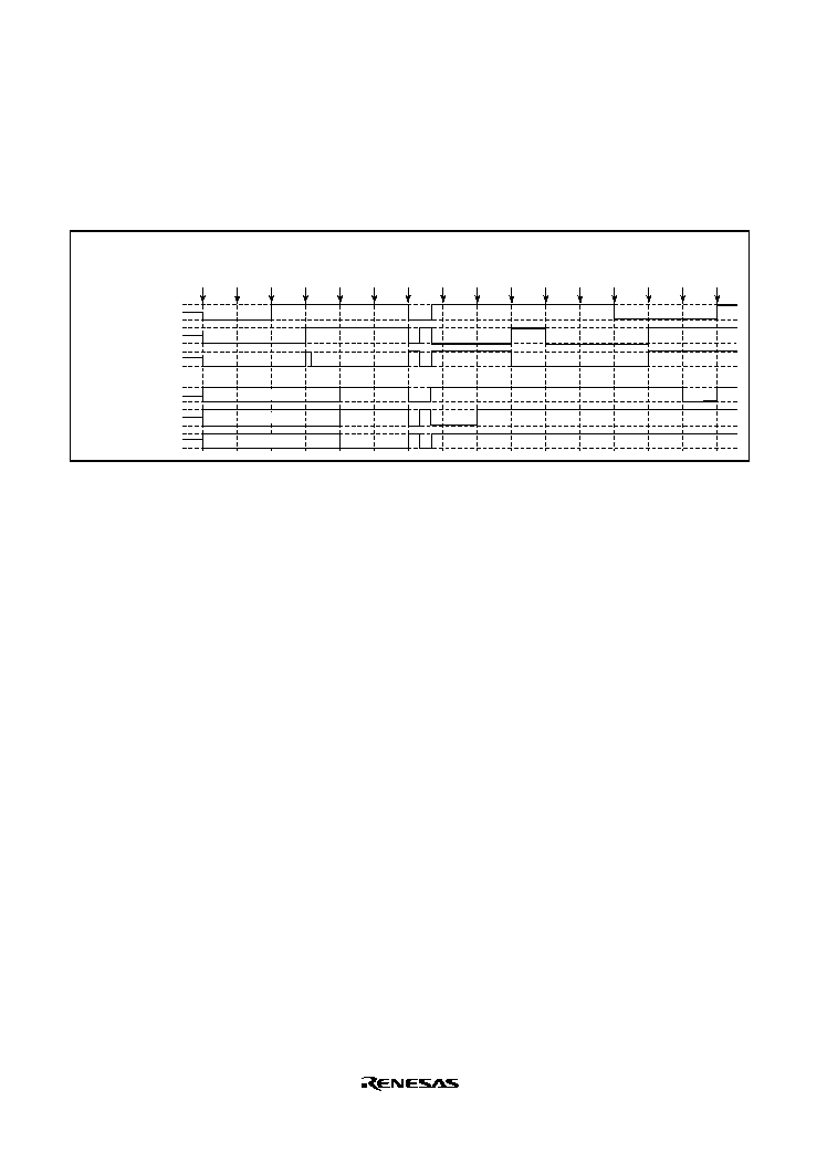
Rev. 2.0, 09/02, page 336 of 732
Operation when Error Occurs during Reset-Synchronous PWM Mode Operation, and
Operation is Restarted in Complementary PWM Mode: Figure 11.112 shows an explanatory
diagram of the case where an error occurs in reset-synchronous PWM mode and operation is
restarted in complementary PWM mode after re-setting.
1
RESET
2
TOCR
3
TMDR
(RPWM)
5
PFC
(MTU)
4
TOER
(1)
6
TSTR
(1)
7
Match
8
Error
occurs
9
PFC
(PORT)
10
TSTR
(0)
11
TOER
(0)
12
TOCR
13
TMDR
(CPWM)
14
TOER
(1)
15
PFC
(MTU)
16
TSTR
(1)
MTU module output
TIOC3A
TIOC3B
TIOC3D
Port output
PE9
PE8
PE11
High-Z
High-Z
High-Z
Figure 11.112 Error Occurrence in Reset-Synchronous PWM Mode,
Recovery in Complementary PWM Mode
1 to 10 are the same as in figure 11.110.
11. Disable channel 3 and 4 output with TOER.
12. Select the complementary PWM output level and cyclic output enabling/disabling with
TOCR.
13. Set complementary PWM. (The MTU cyclic output pin goes low.)
14. Enable channel 3 and 4 output with TOER.
15. Set MTU output with the PFC.
16. Operation is restarted by TSTR.
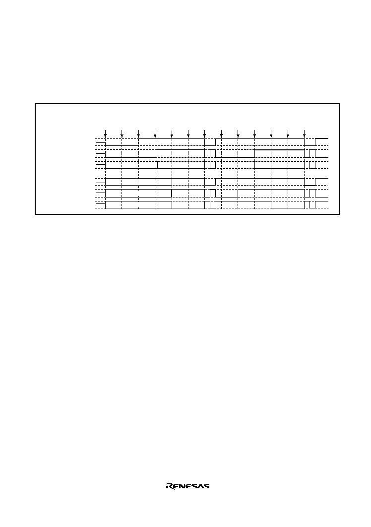
Rev. 2.0, 09/02, page 337 of 732
Operation when Error Occurs during Reset-Synchronous PWM Mode Operation, and
Operation is Restarted in Reset-Synchronous PWM Mode: Figure 11.113 shows an
explanatory diagram of the case where an error occurs in reset-synchronous PWM mode and
operation is restarted in reset-synchronous PWM mode after re-setting.
1
RESET
2
TOCR
3
TMDR
(RPWM)
5
PFC
(MTU)
4
TOER
(1)
6
TSTR
(1)
7
Match
8
Error
occurs
9
PFC
(PORT)
10
TSTR
(0)
11
PFC
(MTU)
12
TSTR
(1)
13
Match
MTU module output
TIOC3A
TIOC3B
TIOC3D
Port output
PE9
PE8
PE11
High-Z
High-Z
High-Z
High-Z
High-Z
High-Z
Figure 11.113 Error Occurrence in Reset-Synchronous PWM Mode,
Recovery in Reset-Synchronous PWM Mode
1 to 10 are the same as in figure 11.110.
11. Set MTU output with the PFC.
12. Operation is restarted by TSTR.
13. The reset-synchronous PWM waveform is output on compare-match occurrence.

Rev. 2.0, 09/02, page 338 of 732
11.9
Port Output Enable (POE)
The port output enable (POE) can be used to establish a high-impedance state for high-current
pins, by changing the
POE0 to POE3 pin input, depending on the output status of the high-current
pins (PE9/TIOC3B/SCK3/
TRST*, PE11/TIOC3D/RXD3/TDO*, PE12/TIOC4A/TXD3/TCK*,
PE13/TIOC4B/
MRES, PE14/TIOC4C/DACK0, PE15/TIOC4D/DACK1/IRQOUT). It can also
simultaneously generate interrupt requests.
The high-current pins can also be set to high-impedance regardless of whether these pin functions
are selected in cases such as when the oscillator stops or in software standby mode. For details,
refer to section 17.1.11, High-Current Port Control Register (PPCR).
However, when using the E10A, the high-impedance function is disabled when an oscillation stop
is detected, port output enable (POE), or in the software standby state for the three pins of
PE9/TIOC3B/SCK3/
TRST, PE11/TIOC3D/RXD3/TDO, and PE12/TIOC4A/TXD3/TCK of the
SH7145.
Note: * Only in the SH7145.
11.9.1
Features
∑
Each of the
POE0 to POE3 input pins can be set for falling edge, P
/8
◊
16, P
/16
◊
16, or
P
/128
◊
16 low-level sampling.
∑
High-current pins can be set to high-impedance state by
POE0 to POE3 pin falling-edge or
low-level sampling.
∑
High-current pins can be set to high-impedance state when the high-current pin output levels
are compared and simultaneous low-level output continues for one cycle or more.
∑
Interrupts can be generated by input-level sampling or output-level comparison results.
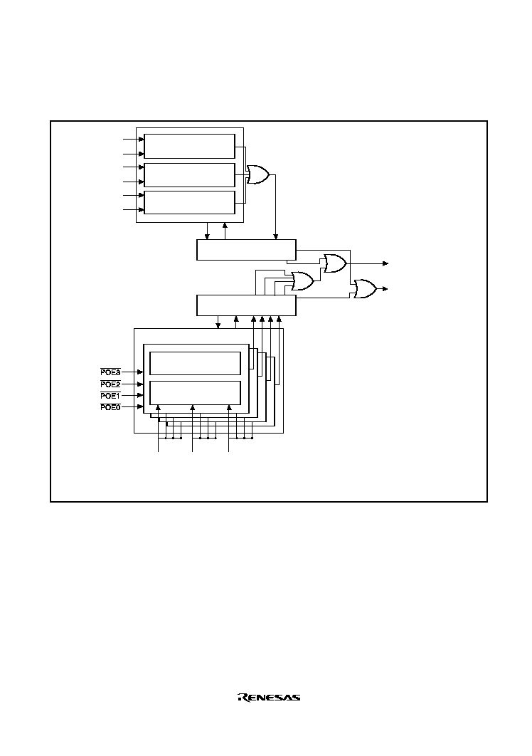
Rev. 2.0, 09/02, page 339 of 732
The POE has input-level detection circuitry and output-level detection circuitry, as shown in the
block diagram of figure 11.114.
TIOC3B
TIOC3D
TIOC4A
TIOC4C
TIOC4B
TIOC4D
Output level
detection circuit
Output level
detection circuit
Output level
detection circuit
Input level detection circuit
Falling-edge
detection circuit
Low-level
detection circuit
OCSR
ICSR1
/8
/16
/128
High-
impedance
request control
signal
Interrupt request
Legend:
OCSR: Output level control/status register
ICSR1: Input level control/status register
Figure 11.114 POE Block Diagram

Rev. 2.0, 09/02, page 340 of 732
11.9.2
Pin Configuration
Table 11.44 Pin Configuration
Name
Abbreviation
I/O
Description
Port output enable input pins
POE0
to
POE3
Input
Input request signals to make high-
current pins high-impedance state
Table 11.45 shows output-level comparisons with pin combinations.
Table 11.45 Pin Combinations
Pin Combination
I/O
Description
PE9/TIOC3B and PE11/TIOC3D
Output
All high-current pins are made high-impedance
state when the pins simultaneously output low-level
for longer than 1 cycle.
PE12/TIOC4A and PE14/TIOC4C
Output
All high-current pins are made high-impedance
state when the pins simultaneously output low-level
for longer than 1 cycle.
PE13/TIOC4B/
MRES
and
PE15/TIOC4D/
IRQOUT
Output
All high-current pins are made high-impedance
state when the pins simultaneously output low-level
for longer than 1 cycle.
11.9.3
Register Descriptions
The POE has the two registers. The input level control/status register 1 (ICSR1) controls both
POE0 to POE3 pin input signal detection and interrupts. The output level control/status register
(OCSR) controls both the enable/disable of output comparison and interrupts.
Input Level Control/Status Register 1 (ICSR1): The input level control/status register (ICSR1)
is a 16-bit readable/writable register that selects the
POE0 to POE3 pin input modes, controls the
enable/disable of interrupts, and indicates status.

Rev. 2.0, 09/02, page 341 of 732
Bit
Bit Name Initial value
R/W
Description
15
POE3F
0
R/(W)
*
POE3 Flag
This flag indicates that a high impedance request has
been input to the
POE3
pin
Clear condition:
∑
By writing 0 to POE3F after reading a POE3F = 1
Set condition:
∑
When the input set by ICSR1 bits 7 and 6 occurs
at the
POE3
pin
14
POE2F
0
R/(W)
*
POE2 Flag
This flag indicates that a high impedance request has
been input to the
POE2
pin
Clear condition:
∑
By writing 0 to POE2F after reading a POE2F = 1
Set condition:
∑
When the input set by ICSR1 bits 5 and 4 occurs
at the
POE2
pin
13
POE1F
0
R/(W)
*
POE1 Flag
This flag indicates that a high impedance request has
been input to the
POE1
pin
Clear condition:
∑
By writing 0 to POE1F after reading a POE1F = 1
Set condition:
∑
When the input set by ICSR1 bits 3 and 2 occurs
at the
POE1
pin
12
POE0F
0
R/(W)
*
POE0 Flag
This flag indicates that a high impedance request has
been input to the
POE0
pin
Clear condition:
∑
By writing 0 to POE0F after reading a POE0F = 1
Set condition:
∑
When the input set by ICSR1 bits 1 and 0 occurs
at the
POE0
pin
11 to 9
All 0
R
Reserved
These bits are always read as 0s and should always
be written with 0s.

Rev. 2.0, 09/02, page 342 of 732
Bit
Bit Name Initial value
R/W
Description
8
PIE
0
R/W
Port Interrupt Enable
This bit enables/disables interrupt requests when any
of the POE0F to POE3F bits of the ICSR1 are set to 1
0: Interrupt requests disabled
1: Interrupt requests enabled
7
6
POE3M1
POE3M0
0
0
R/W
R/W
POE3 mode 1, 0
These bits select the input mode of the
POE3
pin
00: Accept request on falling edge of
POE3
input
01: Accept request when
POE3
input has been
sampled for 16 P
/8 clock pulses, and all are low
level.
10: Accept request when
POE3
input has been
sampled for 16 P
/16 clock pulses, and all are
low level.
11: Accept request when
POE3
input has been
sampled for 16 P
/128 clock pulses, and all are
low level.
5
4
POE2M1
POE2M0
0
0
R/W
R/W
POE2 mode 1, 0
These bits select the input mode of the
POE2
pin
00: Accept request on falling edge of
POE2
input
01: Accept request when
POE2
input has been
sampled for 16 P
/8 clock pulses, and all are low
level.
10: Accept request when
POE2
input has been
sampled for 16 P
/16 clock pulses, and all are
low level.
11: Accept request when
POE2
input has been
sampled for 16 P
/128 clock pulses, and all are
low level.

Rev. 2.0, 09/02, page 343 of 732
Bit
Bit Name Initial value
R/W
Description
3
2
POE1M1
POE1M0
0
0
R/W
R/W
POE1 mode 1, 0
These bits select the input mode of the
POE1
pin
00: Accept request on falling edge of
POE1
input
01: Accept request when
POE1
input has been
sampled for 16 P
/8 clock pulses, and all are low
level.
10: Accept request when
POE1
input has been
sampled for 16 P
/16 clock pulses, and all are
low level.
11: Accept request when
POE1
input has been
sampled for 16 P
/128 clock pulses, and all are
low level.
1
0
POE0M1
POE0M0
0
0
R/W
R/W
POE0 mode 1, 0
These bits select the input mode of the
POE0
pin
00: Accept request on falling edge of
POE0
input
01: Accept request when
POE0
input has been
sampled for 16 P
/8 clock pulses, and all are low
level.
10: Accept request when
POE0
input has been
sampled for 16 P
/16 clock pulses, and all are
low level.
11: Accept request when
POE0
input has been
sampled for 16 P
/128 clock pulses, and all are
low level.
Note:
*
Only 0 can be written to clear the flag.

Rev. 2.0, 09/02, page 344 of 732
Output Level Control/Status Register (OCSR): The output level control/status register (OCSR)
is a 16-bit readable/writable register that controls the enable/disable of both output level
comparison and interrupts, and indicates status. If the OSF bit is set to 1, the high current pins
become high impedance.
Bit
Bit Name
Initial value
R/W
Description
15
OSF
0
R/(W)
*
Output Short Flag
This flag indicates that any one pair of the three
pairs of 2 phase outputs compared have
simultaneously become low level outputs.
Clear condition:
∑
By writing 0 to OSF after reading an OSF = 1
Set condition:
∑
When any one pair of the three 2-phase outputs
simultaneously become low level
14 to
10
All 0
R
Reserved
These bits are always read as 0s and should always
be written with 0s.
9
OCE
0
R/W
Output Level Compare Enable
This bit enables the start of output level
comparisons. When setting this bit to 1, pay
attention to the output pin combinations shown in
table 11.43, Mode Transition Combinations. When 0
is output, the OSF bit is set to 1 at the same time
when this bit is set, and output goes to high
impedance. Accordingly, bits 15 to 11 and bit 9 of
the port E data register (PEDR) are set to 1. For the
MTU output comparison, set the bit to 1 after setting
the MTU's output pins with the PFC. Set this bit only
when using pins as outputs.
When the OCE bit is set to 1, if OIE = 0 a high-
impedance request will not be issued even if OSF is
set to 1. Therefore, in order to have a high-
impedance request issued according to the result of
the output level comparison, the OIE bit must be set
to 1. When OCE = 1 and OIE = 1, an interrupt
request will be generated at the same time as the
high-impedance request: however, this interrupt can
be masked by means of an interrupt controller
(INTC) setting.
0: Output level compare disabled
1: Output level compare enabled; makes an output
high impedance request when OSF = 1.

Rev. 2.0, 09/02, page 345 of 732
Bit
Bit Name
Initial value
R/W
Description
8
OIE
0
R/W
Output Short Interrupt Enable
This bit makes interrupt requests when the OSF bit
of the OCSR is set.
00: Interrupt requests disabled
01: Interrupt request enabled
7 to 0
All 0
R
Reserved
These bits are always read as 0s and should always
be written with 0s.
Note:
*
Only 0 can be written to write the flag.
11.9.4
Operation
Input Level Detection Operation
If the input conditions set by the ICSR1 occur on any of the
POE pins, all high-current pins
become high-impedance state. Note however, that these high-current pins become high-impedance
state only when general input/output function or MTU function is selected in these pins.
Falling Edge Detection: When a change from high to low level is input to the
POE pins.
Low-Level Detection: Figure 11.115 shows the low-level detection operation. Sixteen continuous
low levels are sampled with the sampling clock established by the ICSR1. If even one high level is
detected during this interval, the low level is not accepted.
Sampling starts when detecting the falling edge of the
POE pin. Thereby, negate the POE pin
when using
POE function after sampling.
Furthermore, the timing when the large-current pins enter the high-impedance state from the
sampling clock is the same in both falling-edge detection and in low-level detection.
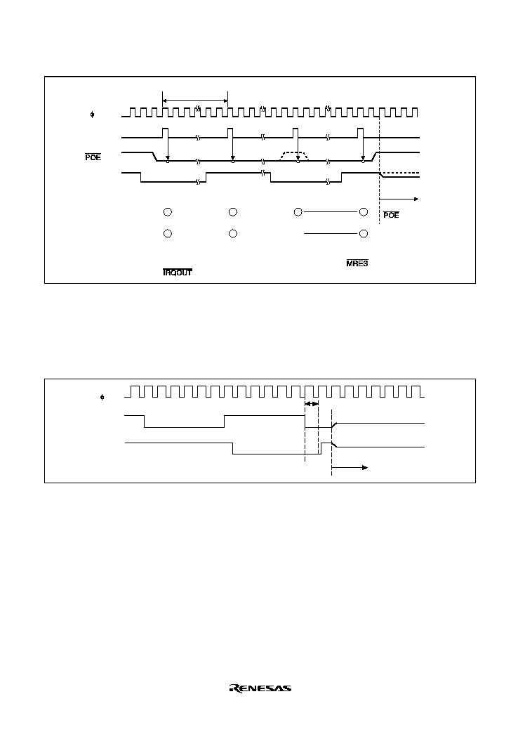
Rev. 2.0, 09/02, page 346 of 732
P
Sampling
clock
3
input
PE9/
TIOC3B
When low level is
sampled at all points
When high level is
sampled at least once
Flag set
(
received)
Flag not set
High-impedance
state
*
Note:
*
Other large-current pins (PE11/TIOC3D, PE12/TIOC4A, PE13/TIOC4B/
, PE14/TIOC4C,
PE15/TIOC4D/
) also go to the high-impedance state at the same timing.
2
1
2
1
16
13
8/16/128 clock
cycles
Figure 11.115 Low-Level Detection Operation
Output-Level Compare Operation
Figure 11.116 shows an example of the output-level compare operation for the combination of
PE9/TIOC3B and PE11/TIOC3D. The operation is the same for the other pin combinations.
P
PE11/
TIOC3D
PE9/
TIOC3B
Low level overlapping detected
High impedance state
Figure 11.116 Output-Level Detection Operation
Release from High-Impedance State
High-current pins that have entered high-impedance state due to input-level detection can be
released either by returning them to their initial state with a power-on reset, or by clearing all of
the bit 12 to 15 (POE0F to POE3F) flags of the ICSR1. High-current pins that have become high-
impedance due to output-level detection can be released either by returning them to their initial
state with a power-on reset, or by first clearing bit 9 (OCE) of the OCSR to disable output-level
compares, then clearing the bit 15 (OSF) flag. However, when returning from high-impedance
state by clearing the OSF flag, always do so only after outputting a high level from the high-
current pins (TIOC3B, TIOC3D, TIOC4A, TIOC4B, TIOC4C, and TIOC4D). High-level outputs
can be achieved by setting the MTU internal registers.
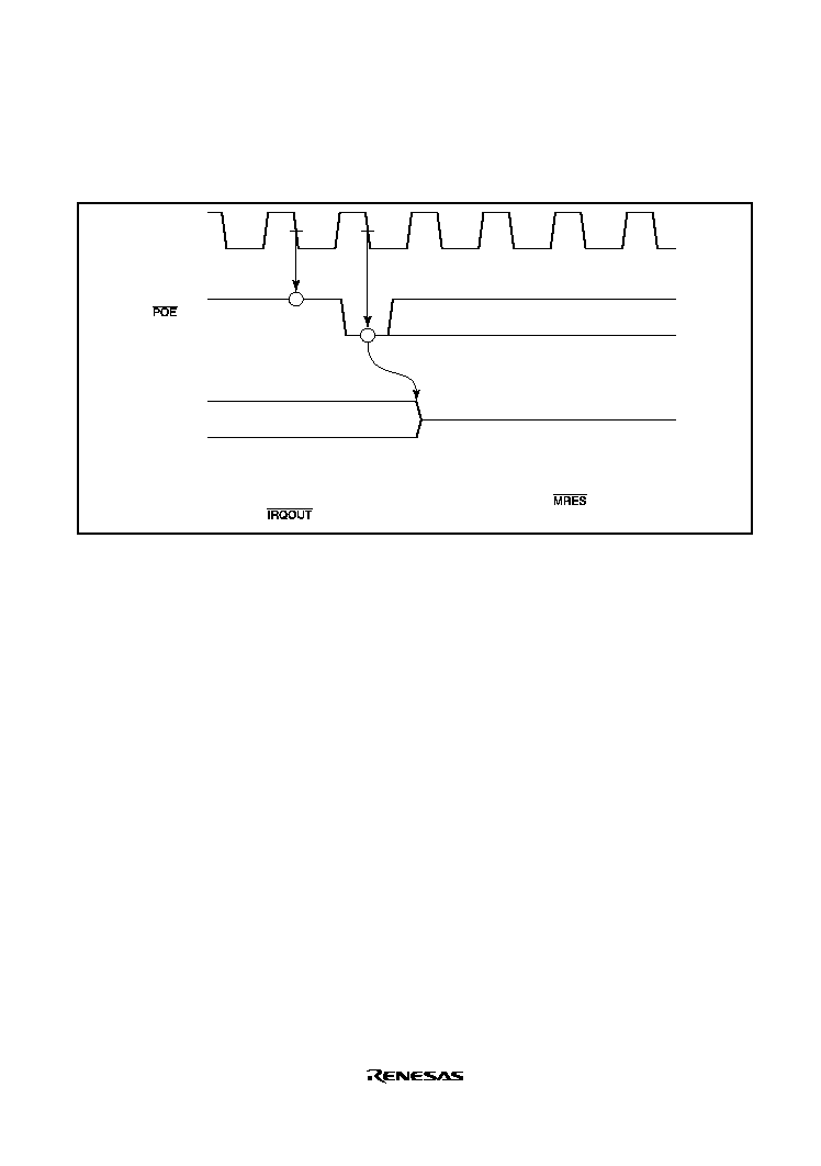
Rev. 2.0, 09/02, page 347 of 732
POE Timing
Figure 11.117 shows an example of timing from
POE input to high impedance of pin.
input
CK falling
CK
PE9/
TIOC3B
Falling edge detected
High impedance state
Note: Other large-current pins (PE11/TIOC3D, PE12/TIOC4A, PE13/TIOC4B/
, PE14/TIOC4C,
PE15/TIOC4D/
) also goes to the high impedance state at the same timing
Figure 11.117 Falling Edge Detection Operation
11.9.5
Usage Note
Make sure to set the input to the
POE pin high, before detecting the level of the POE pin.

Rev. 2.0, 09/02, page 348 of 732

WDT0400A_020020020700
Rev. 2.0, 09/02, page 349 of 732
Section 12 Watchdog Timer
The watchdog timer (WDT) is an 8-bit timer that can generate an internal reset signal for this LSI
if a system crash prevents the CPU from writing to the timer counter, thus it causes the overflow.
When this watchdog function is not needed, the WDT can be used as an interval timer. In interval
timer operation, an interval timer interrupt is generated each time the counter overflows.
The block diagram of the WDT is shown in figure 12.1.
12.1
Features
∑
Selectable from eight counter input clocks.
∑
Switchable between watchdog timer mode and interval timer mode
∑
Clears software standby mode
In watchdog timer mode
∑
Output
WDTOVF signal
∑
Selectable whether this LSI is internally reset or not.
In interval timer mode
∑
If the counter overflows, the WDT generates an interval timer interrupt (ITI).
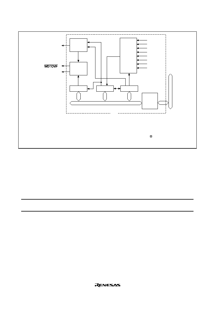
Rev. 2.0, 09/02, page 350 of 732
Overflow
Interrupt
control
ITI (interrupt
request signal)
Internal reset
signal
*
2
Reset
control
RSTCSR
TCNT
TSCR
/2
/64
/128
/256
/512
/1024
/4096
/8192
Clock
Clock
select
Internal clock
sources
Bus
interface
Module bus
Internal bus
WDT
Legend:
TCSR:
Timer control/status register
TCNT: Timer
counter
RSTCSR: Reset control/status register
Notes: 1.
If this pin needs to be pulled-down,the resistance value must be 1M or higher.
2.
The internal reset signal can be generated by register setting.
Power-on reset or manual reset can be selected.
*
1
Figure 12.1 Block Diagram of WDT
12.2
Input/Output Pin
Table 12.1 shows the pin configuration.
Table 12.1 Pin Configuration
Pin
Abbreviation
I/O
Function
Watchdog timer overflow
WDTOVF
Output
Outputs the counter overflow signal in
watchdog timer mode
12.3
Register Descriptions
The WDT has the following three registers. For details, refer to section 25, List of Registers. To
prevent accidental overwriting, TCSR, TCNT, and RSTCSR have to be written to in a method
different from normal registers. For details, refer to section 12.6.1, Notes on Register Access.
∑
Timer control/status register (TCSR)
∑
Timer counter (TCNT)
∑
Reset control/status register (RSTCSR)

Rev. 2.0, 09/02, page 351 of 732
12.3.1
Timer Counter (TCNT)
TCNT is an 8-bit readable/writable upcounter. When the timer enable bit (TME) in the timer
control/status register (TCSR) is set to 1, TCNT starts counting pulses of an internal clock selected
by clock select bits 2 to 0 (CKS2 to CKS0) in TCSR. When the value of TCNT overflows
(changes from H'FF to H'00), a watchdog timer overflow signal (
WDTOVF) or interval timer
interrupt (ITI) is generated, depending on the mode selected in the WT/
IT bit of TCSR.
The initial value of TCNT is H
00.
12.3.2
Timer Control/Status Register (TCSR)
TCSR is an 8-bit readable/writable register. Its functions include selecting the clock source to be
input to TCNT, and the timer mode.
Bit
Bit Name
Initial Value
R/W
Description
7
OVF
0
R/(W)
*
1
Overflow Flag
Indicates that TCNT has overflowed in interval timer
mode. Only a write of 0 is permitted, to clear the
flag. This flag is not set in watchdog timer mode.
[Setting condition]
∑
When TCNT overflows in interval timer mode.
[Clearing condition]
∑
When writing 0 to this bit after reading this bit or
when writing 0 to the TME bit in interval timer
mode.
6
WT/
IT
0
R/W
Timer Mode Select
Selects whether the WDT is used as a watchdog
timer or interval timer. When TCNT overflows, the
WDT either generates an interval timer interrupt (ITI)
or generates a
WDTOVF
signal, depending on the
mode selected.
0: Interval timer mode
Interval timer interrupt (ITI) request to the CPU
when TCNT overflows
1: Watchdog timer mode
WDTOVF
signal output externally when TCNT
overflows.
For details on the TCNT overflow in watchdog
timer mode, refer to section 12.3.3, Reset
Control/Status Register (RSTCSR).

Rev. 2.0, 09/02, page 352 of 732
Bit
Bit Name
Initial Value
R/W
Description
5
TME
0
R/W
Timer Enable
Enables or disables the timer.
0: Timer disabled
TCNT is initialized to H'00 and count-up stops
1: Timer enabled
TCNT starts counting. A
WDTOVF
signal or
interrupt is generated when TCNT overflows.
4
3
--
--
1
1
R
R
Reserved
This bit is always read as 1 and cannot be modified.
2
1
0
CKS2
CKS1
CKS0
0
0
0
R/W
R/W
R/W
Clock Select 2 to 0
Select one of eight internal clock sources for input to
TCNT. The clock signals are obtained by dividing the
frequency of the system clock (
). The overflow
frequency for
= 40 MHz is enclosed in
parentheses
*
2
.
000: Clock
/2 (overflow interval: 12.8
µ
s)
001: Clock
/64 (overflow interval: 409.6
µ
s)
010: Clock
/128 (overflow interval: 0.8 ms)
011: Clock
/256 (overflow interval: 1.6 ms)
100: Clock
/512 (overflow interval: 3.3 ms)
101: Clock
/1024 (overflow interval: 6.6 ms)
110: Clock
/4096 (overflow interval: 26.2 ms)
111: Clock
/8192 (overflow interval: 52.4 ms)
Notes: 1. Only a 0 can be written after reading 1.
2. The overflow interval listed is the time from when the TCNT begins counting at H'00
until an overflow occurs.

Rev. 2.0, 09/02, page 353 of 732
12.3.3
Reset Control/Status Register (RSTCSR)
RSTCSR is an 8-bit readable/writable register that controls the generation of the internal reset
signal when TCNT overflows, and selects the type of internal reset signal.
Bit
Bit Name
Initial Value
R/W
Description
7
WOVF
0
R/(W)
*
Watchdog Timer Overflow Flag
This bit is set when TCNT overflows in watchdog
timer mode. This bit cannot be set in interval timer
mode.
[Setting condition]
∑
Set when TCNT overflows in watchdog timer
mode
[Clearing condition]
∑
Cleared by reading WOVF, and then writing 0 to
WOVF
6
RSTE
0
R/W
Reset Enable
Specifies whether or not an internal reset signal is
generated in the chip if TCNT overflows in watchdog
timer mode.
0: Internal reset signal is not generated even if
TCNT overflows
(Though this LSI is not reset, TCNT and TCSR in
WDT are reset)
1: Internal reset signal is generated if TCNT
overflows
5
RSTS
0
R/W
Reset Select
Selects the type of internal reset generated if TCNT
overflows in watchdog timer mode.
0: Power-on reset
1: Manual reset
4
3
2
1
0
--
--
--
--
--
1
1
1
1
1
R
R
R
R
R
Reserved
These bits are always read as 1 and cannot be
modified.
Note:
*
Only 0 can be written, for flag clearing.

Rev. 2.0, 09/02, page 354 of 732
12.4
Operation
12.4.1
Watchdog Timer Mode
To use the WDT as a watchdog timer, set the WT/
IT and TME bits of TCSR to 1. Software must
prevent TCNT overflow by rewriting the TCNT value (normally by writing H'00) before overflow
occurs. No TCNT overflows will occur while the system is operating normally, but if TCNT fails
to be rewritten and overflows occur due to a system crash or the like, a
WDTOVF signal is output
externally. The
WDTOVF signal can be used to reset the system. The WDTOVF signal is output
for 128
clock cycles.
If the RSTE bit in RSTCSR is set to 1, a signal to reset the chip will be generated internally
simultaneous to the
WDTOVF signal when TCNT overflows. Either a power-on reset or a manual
reset can be selected by the RSTS bit in RSTCSR. The internal reset signal is output for 512
clock cycles.
When a WDT overflow reset is generated simultaneously with a reset input at the
RES pin, the
RES reset takes priority, and the WOVF bit in RSTCSR is cleared to 0.
The following are not initialized by a WDT reset signal:
∑
POE (port output enable) of MTU registers
∑
PFC (pin function controller) registers
∑
I/O port registers
These registers are initialized only by an external power-on reset.

Rev. 2.0, 09/02, page 355 of 732
TCNT value
H'FF
H'00
signal
Internal reset
signal
*
Overflow
H'00 written
in TCNT
WT/ = 1
TME = 1
H'00 written
in TCNT
WT/ = 1
TME = 1
WOVF = 1
and internal
reset generated
128
clocks
512
clocks
WT/ : Timer mode select bit
TME:
Timer enable bit
Note:
*
Internal reset signal occurs only when the RSTE bit is set to 1.
Time
Figure 12.2 Operation in Watchdog Timer Mode
12.4.2
Interval Timer Mode
To use the WDT as an interval timer, clear WT/
IT to 0 and set TME to 1 in TCSR. An interval
timer interrupt (ITI) is generated each time the timer counter (TCNT) overflows. This function can
be used to generate interval timer interrupts at regular intervals.
TCNT value
H'FF
H'00
Overflow
WT/ = 0
TME = 1
Overflow
Overflow
Overflow
ITI
ITI
ITI
ITI
Time
ITI: Interval timer interrupt request generation
Figure 12.3 Operation in Interval Timer Mode
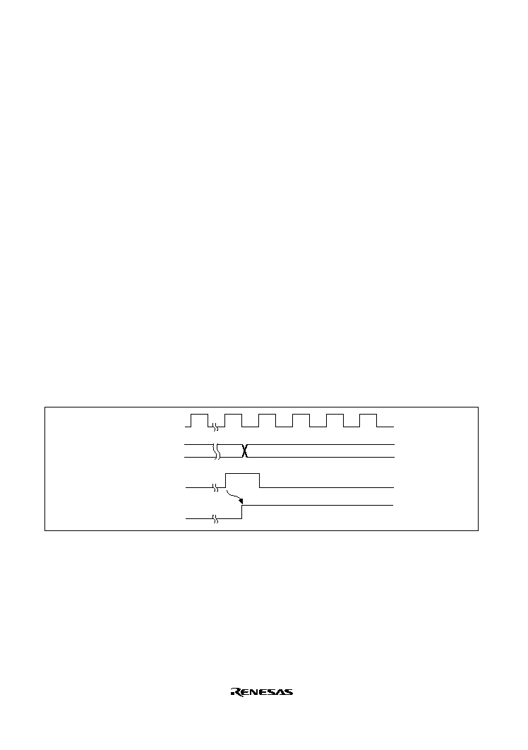
Rev. 2.0, 09/02, page 356 of 732
12.4.3
Clearing Software Standby Mode
The watchdog timer has a special function to clear software standby mode with an NMI interrupt
or
IRQ0 to IRQ7 interrupts. When using software standby mode, set the WDT as described below.
Before Transition to Software Standby Mode: The TME bit in TCSR must be cleared to 0 to
stop the watchdog timer counter before entering software standby mode. The chip cannot enter
software standby mode while the TME bit is set to 1. Set bits CKS2 to CKS0 in TCSR so that the
counter overflow interval is equal to or longer than the oscillation settling time. See section 26.3,
AC Characteristics, for the oscillation settling time.
Recovery from Software Standby Mode: When an NMI signal or
IRQ0 to IRQ7 signals are
received in software standby mode, the clock oscillator starts running and TCNT starts
incrementing at the rate selected by bits CKS2 to CKS0 before software standby mode was
entered. When TCNT overflows (changes from H'FF to H'00), the clock is presumed to be stable
and usable; clock signals are supplied to the entire chip and software standby mode ends.
For details on software standby mode, see section 24, Power-Down States.
12.4.4
Timing of Setting the Overflow Flag (OVF)
In interval timer mode, when TCNT overflows, the OVF bit of TCSR is set to 1 and an interval
timer interrupt (ITI) is simultaneously requested. Figure 12.4 shows this timing.
TCNT
Overflow signal
(internal signal)
OVF
H'FF
H'00
Figure 12.4 Timing of Setting OVF
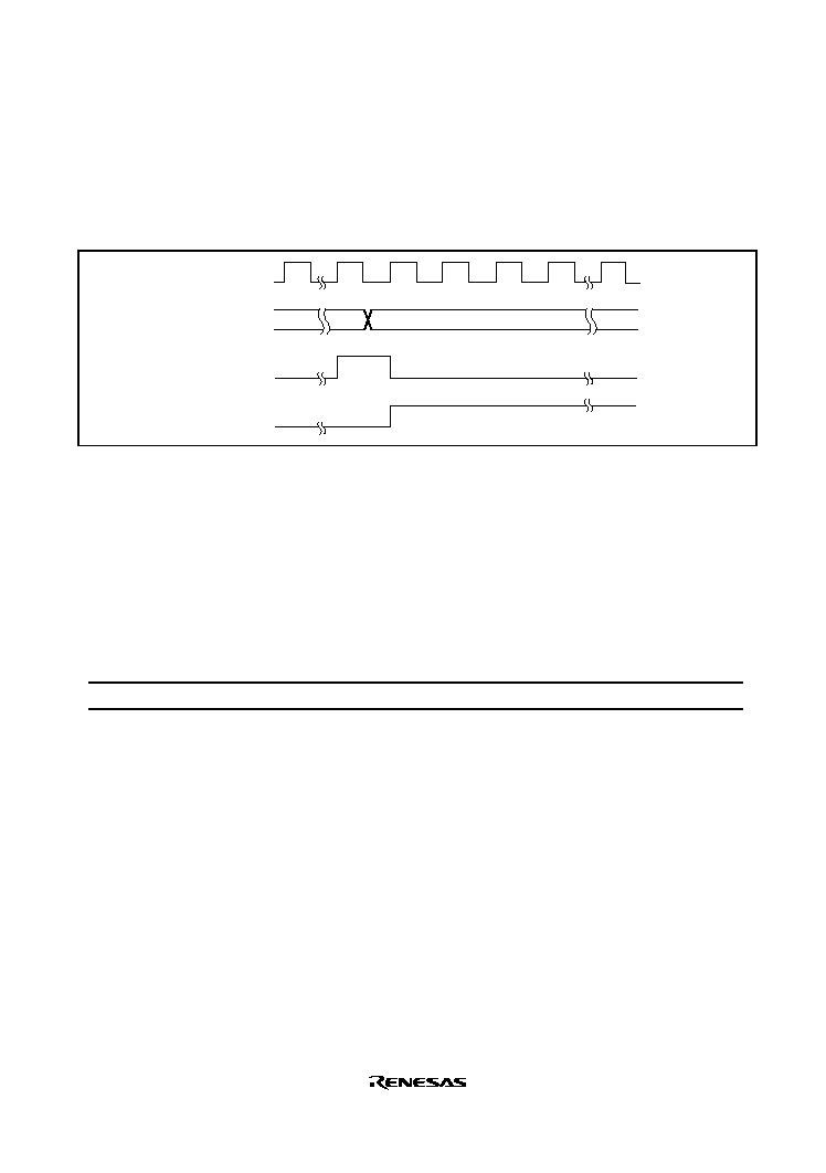
Rev. 2.0, 09/02, page 357 of 732
12.4.5
Timing of Setting the Watchdog Timer Overflow Flag (WOVF)
When TCNT overflows in watchdog timer mode, the WOVF bit of RSTCSR is set to 1 and a
WDTOVF signal is output. When the RSTE bit in RSTCSR is set to 1, TCNT overflow enables an
internal reset signal to be generated for the entire chip. Figure 12.5 shows this timing.
TCNT
Overflow signal
(internal signal)
WOVF
H'FF
H'00
Figure 12.5 Timing of Setting WOVF
12.5
Interrupt Sources
During interval timer mode operation, an overflow generates an interval timer interrupt (ITI). The
interval timer interrupt is requested whenever the OVF flag is set to 1 in TCSR. OVF must be
cleared to 0 in the interrupt handling routine.
Table 12.2 WDT Interrupt Source (in Interval Timer Mode)
Name
Interrupt Source
Interrupt Flag
DMAC/DTC Activation
ITI
TCNT overflow
OVF
Impossible
12.6
Usage Notes
12.6.1
Notes on Register Access
The watchdog timer's TCNT, TCSR, and RSTCSR registers differ from other registers in being
more difficult to write to. The procedures for writing to and reading these registers are given
below.
Writing to TCNT and TCSR: These registers must be written by a word transfer instruction.
They cannot be written by byte transfer instructions.
TCNT and TCSR both have the same write address. The write data must be contained in the lower
byte of the written word. The upper byte must be H'5A (for TCNT) or H'A5 (for TCSR) (figure
12.6). This transfers the write data from the lower byte to TCNT or TCSR.

Rev. 2.0, 09/02, page 358 of 732
15
8
7
0
15
8
7
0
H'5A
H'A5
Write data
Write data
∑ Writing to TCNT
∑ Writing to TCSR
Address: H'FFFF8610
Address: H'FFFF8610
Figure 12.6 Writing to TCNT and TCSR
Writing to RSTCSR: RSTCSR must be written by a word access to address H'FFFF8612. It
cannot be written by byte transfer instructions.
Procedures for writing 0 to WOVF (bit 7) and for writing to RSTE (bit 6) and RSTS (bit 5) are
different, as shown in figure 12.7.
To write 0 to the WOVF bit, the write data must be H'A5 in the upper byte and H'00 in the lower
byte. This clears the WOVF bit to 0. The RSTE and RSTS bits are not affected. To write to the
RSTE and RSTS bits, the upper byte must be H'5A and the lower byte must be the write data. The
values of bits 6 and 5 of the lower byte are transferred to the RSTE and RSTS bits, respectively.
The WOVF bit is not affected.
15
8
7
0
15
8
7
0
H'A5
H'5A
Write data
∑ Writing 0 to the WOVF bit
∑ Writing to the RSTE and RSTS bits
Address: H'FFFF8612
Address: H'FFFF8612
H'00
Figure 12.7 Writing to RSTCSR
Reading from TCNT, TCSR, and RSTCSR: TCNT, TCSR, and RSTCSR are read like other
registers. Use byte transfer instructions. The read addresses are H'FFFF8610 for TCSR,
H'FFFF8611 for TCNT, and H'FFFF8613 for RSTCSR.
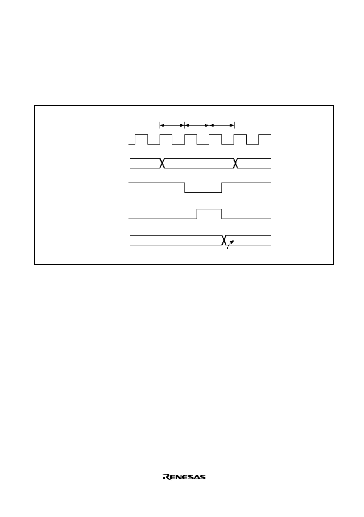
Rev. 2.0, 09/02, page 359 of 732
12.6.2
TCNT Write and Increment Contention
If a timer counter increment clock pulse is generated during the T3 state of a write cycle to TCNT,
the write takes priority and the timer counter is not incremented. Figure 12.8 shows this operation.
Address
Internal write
signal
TCNT input
clock
TCNT
N
M
T1
T2
TCNT write cycle
Counter write data
T3
TCNT address
Figure 12.8 Contention between TCNT Write and Increment
12.6.3
Changing CKS2 to CKS0 Bit Values
If the values of bits CKS2 to CKS0 in the timer control/status register (TCSR) are rewritten while
the WDT is running, the count may not increment correctly. Always stop the watchdog timer (by
clearing the TME bit to 0) before changing the values of bits CKS2 to CKS0.
12.6.4
Changing between Watchdog Timer/Interval Timer Modes
To prevent incorrect operation, always stop the watchdog timer (by clearing the TME bit to 0)
before switching between interval timer mode and watchdog timer mode.
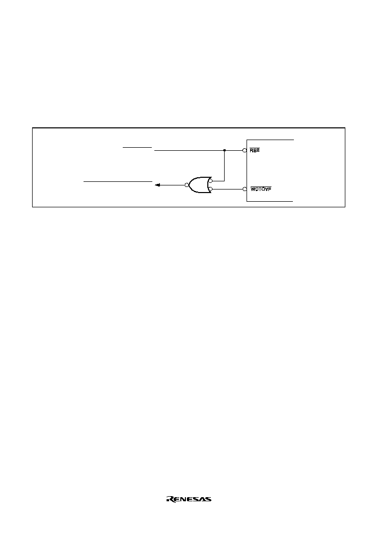
Rev. 2.0, 09/02, page 360 of 732
12.6.5
System Reset by
WDTOVF
WDTOVF
WDTOVF
WDTOVF Signal
If a
WDTOVF output signal is input to the RES pin, the chip cannot initialize correctly.
Avoid to connect the
WDTOVF signal to the RES input pin directly. To reset the entire system
with the
WDTOVF signal, use the circuit shown in figure 12.9.
Reset input
Reset signal to entire system
This LSI
Figure 12.9 Example of System Reset Circuit Using
WDTOVF
WDTOVF
WDTOVF
WDTOVF Signal
12.6.6
Internal Reset in Watchdog Timer Mode
If the RSTE bit is cleared to 0 in watchdog timer mode, the chip will not be reset internally when a
TCNT overflow occurs, but TCNT and TCSR in the WDT will be reset.
12.6.7
Manual Reset in Watchdog Timer Mode
When an internal reset is effected by TCNT overflow in watchdog timer mode, the processor waits
until the end of the bus cycle at the time of manual reset generation before making the transition to
manual reset exception processing. Therefore, the bus cycle is retained in a manual reset, but if a
manual reset occurs while the bus is released, manual reset exception processing will be deferred
until the CPU acquires the bus. However, if the interval from generation of the manual reset until
the end of the bus cycle is equal to or longer than the internal manual reset interval of 512 cycles,
the internal manual reset source is ignored instead of being deferred, and manual reset exception
processing is not executed.

SCIS200B_020020020700
Rev. 2.0, 09/02, page 361 of 732
Section 13 Serial Communication Interface (SCI)
This LSI has four independent serial communication interface (SCI) channels. The SCI can handle
both asynchronous and clocked synchronous serial communication. Serial data communication
can be carried out with standard asynchronous communication chips such as a Universal
Asynchronous Receiver/Transmitter (UART) or Asynchronous Communication Interface Adapter
(ACIA). A function is also provided for serial communication between processors (multiprocessor
communication function).
13.1
Features
∑
Choice of asynchronous or clocked synchronous serial communication mode
∑
Full-duplex communication capability
The transmitter and receiver are mutually independent, enabling transmission and reception to
be executed simultaneously.
Double-buffering is used in both the transmitter and the receiver, enabling continuous
transmission and continuous reception of serial data.
∑
On-chip baud rate generator allows any bit rate to be selected
External clock can be selected as a transfer clock source.
∑
Choice of LSB-first or MSB-first transfer* (except in the case of asynchronous mode 7-bit
data)
∑
Four interrupt sources
Four interrupt sources -- transmit-end, transmit-data-empty, receive-data-full, and receive
error -- that can issue requests.
The transmit-data-empty interrupt and receive data full interrupts can activate the direct
memory access controller (DMAC) and the data transfer controller (DTC).
∑
Module standby mode can be set
Asynchronous mode
∑
Data length: 7 or 8 bits
∑
Stop bit length: 1 or 2 bits
∑
Parity: Even, odd, or none
∑
Multiprocessor bit: 1 or none
∑
Receive error detection: Parity, overrun, and framing errors
∑
Break detection: Break can be detected by reading the RxD pin level directly in case of a
framing error
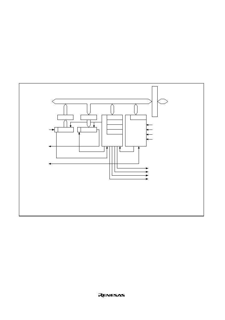
Rev. 2.0, 09/02, page 362 of 732
Clocked Synchronous mode
∑
Data length: 8 bits
∑
Receive error detection: Overrun errors detected
Note: * The description in this section are based on LSB-first transfer.
Figure 13.1 shows a block diagram of the SCI.
RxD
TxD
SCK
Clock
P
P
/8
P
/32
P
/128
TEI
TXI
RXI
ERI
SSR
SCR
SMR
SDCR
Transmission/
reception
control
Baud rate
generator
BRR
Module data bus
RDR
TSR
RSR
Parity generation
Legend:
RSR:
Receive shift register
RDR: Receive data register
TSR:
Transmit shift register
TDR:
Transmit data register
SMR: Serial mode register
SCR:
Serial control register
SSR:
Serial status register
BRR:
Bit rate register
SDCR: Serial direction control register
TDR
Bus interface
Internal
data bus
Parity check
External clock
Figure 13.1 Block Diagram of SCI

Rev. 2.0, 09/02, page 363 of 732
13.2
Input/Output Pins
Table 13.1 shows the pins for each SCI channel.
Table 13.1 Pin Configuration
Channel
Pin Name
*
I/O
Function
SCK0
I/O
SCI0 clock input/output
RxD0
Input
SCI0 receive data input
0
TxD0
Output
SCI0 transmit data output
SCK1
I/O
SCI1 clock input/output
RxD1
Input
SCI1 receive data input
1
TxD1
Output
SCI1 transmit data output
SCK2
I/O
SCI2 clock input/output
RxD2
Input
SCI2 receive data input
2
TxD2
Output
SCI2 transmit data output
SCK3
I/O
SCI3 clock input/output
RxD3
Input
SCI3 receive data input
3
TxD3
Output
SCI3 transmit data output
Notes:
*
Pin names SCK, RxD, and TxD are used in the text for all channels, omitting the channel
1 designation.
13.3
Register Descriptions
The SCI has the following registers for each channel. For details on register addresses and register
states during each processing, refer to section 25, List of Registers.
Channel 0
∑
Serial mode register_0 (SMR_0)
∑
Bit rate register_0 (BRR_0)
∑
Serial control register_0 (SCR_0)
∑
Transmit data register_0 (TDR_0)
∑
Serial status register_0 (SSR_0)
∑
Receive data register_0 (RDR_0)
∑
Serial direction control register_0 (SDCR_0)

Rev. 2.0, 09/02, page 364 of 732
Channel 1
∑
Serial mode register_1 (SMR_1)
∑
Bit rate register_1 (BRR_1)
∑
Serial control register_1 (SCR_1)
∑
Transmit data register_1 (TDR_1)
∑
Serial status register_1 (SSR_1)
∑
Receive data register_1 (RDR_1)
∑
Serial direction control register_1 (SDCR_1)
Channel 2
∑
Serial mode register_2 (SMR_2)
∑
Bit rate register_2 (BRR_2)
∑
Serial control register_2 (SCR_2)
∑
Transmit data register_2 (TDR_2)
∑
Serial status register_2 (SSR_2)
∑
Receive data register_2 (RDR_2)
∑
Serial direction control register_2 (SDCR_2)
Channel 3
∑
Serial mode register_3 (SMR_3)
∑
Bit rate register_3 (BRR_3)
∑
Serial control register_3 (SCR_3)
∑
Transmit data register_3 (TDR_3)
∑
Serial status register_3 (SSR_3)
∑
Receive data register_3 (RDR_3)
∑
Serial direction control register_3 (SDCR_3)

Rev. 2.0, 09/02, page 365 of 732
13.3.1
Receive Shift Register (RSR)
RSR is a shift register used to receive serial data that is input to the RxD pin and convert it into
parallel data. When one byte of data has been received, it is transferred to RDR automatically.
RSR cannot be directly read or written to by the CPU.
13.3.2
Receive Data Register (RDR)
RDR is an 8-bit register that stores receive data. When the SCI has received one byte of serial
data, it transfers the received serial data from RSR to RDR where it is stored. After this, RSR is
receive-enabled. Since RSR and RDR function as a double buffer in this way, enables continuous
receive operations to be performed. After confirming that the RDRF bit in SSR is set to 1, read
RDR for only once. RDR cannot be written to by the CPU.
The initial value of RDR is H
00.
13.3.3
Transmit Shift Register (TSR)
TSR is a shift register that transmits serial data. To perform serial data transmission, the SCI first
transfers transmit data from TDR to TSR, then sends the data to the TxD pin starting. TSR cannot
be directly accessed by the CPU.
13.3.4
Transmit Data Register (TDR)
TDR is an 8-bit register that stores transmit data. When the SCI detects that TSR is empty, it
transfers the transmit data written in TDR to TSR and starts transmission. The double-buffered
structures of TDR and TSR enables continuous serial transmission. If the next transmit data has
already been written to TDR during serial transmission, the SCI transfers the written data to TSR
to continue transmission. Although TDR can be read or written to by the CPU at all times, to
achieve reliable serial transmission, write transmit data to TDR for only once after confirming that
the TDRE bit in SSR is set to 1.
The initial value of TDR is H
FF.

Rev. 2.0, 09/02, page 366 of 732
13.3.5
Serial Mode Register (SMR)
SMR is used to set the SCI's serial transfer format and select the baud rate generator clock source.
Bit
Bit Name
Initial Value
R/W
Description
7
C/
A
0
R/W
Communication Mode
0: Asynchronous mode
1: Clocked synchronous mode
6
CHR
0
R/W
Character Length (enabled only in asynchronous
mode)
0: Selects 8 bits as the data length.
1: Selects 7 bits as the data length. LSB-first is fixed
and the MSB (bit 7) of TDR is not transmitted in
transmission.
In clocked synchronous mode, a fixed data length of
8 bits is used.
5
PE
0
R/W
Parity Enable (enabled only in asynchronous mode)
When this bit is set to 1, the parity bit is added to
transmit data before transmission, and the parity bit is
checked in reception. For a multiprocessor format,
parity bit addition and checking are not performed
regardless of the PE bit setting.
4
O/
E
0
R/W
Parity Mode (enabled only when the PE bit is 1 in
asynchronous mode)
0: Selects even parity.
1: Selects odd parity.
3
STOP
0
R/W
Stop Bit Length (enabled only in asynchronous mode)
Selects the stop bit length in transmission.
0: 1 stop bit
1: 2 stop bits
In reception, only the first stop bit is checked. If the
second stop bit is 0, it is treated as the start bit of the
next transmit character.
2
MP
0
R/W
Multiprocessor Mode (enabled only in asynchronous
mode)
When this bit is set to 1, the multiprocessor
communication function is enabled. The PE bit and
O/
E
bit settings are invalid in multiprocessor mode.

Rev. 2.0, 09/02, page 367 of 732
Bit
Bit Name
Initial Value
R/W
Description
1
0
CKS1
CKS0
0
0
R/W
R/W
Clock Select 1 and 0
These bits select the clock source for the baud rate
generator.
00: P
clock (n = 0)
01: P
/8 clock (n = 1)
10: P
/32 clock (n = 2)
11: P
/128 clock (n = 3)
For the relation between the setting of CKS1 and
CKS2 and the baud rate, see section 13.3.9, Bit Rate
Register (BRR). n is the decimal display of the value
of n in BRR (see section 13.3.9, Bit Rate Register
(BRR)).
13.3.6
Serial Control Register (SCR)
SCR is a register that performs enabling or disabling of SCI transfer operations and interrupt
requests, and selection of the transfer clock source. For details on interrupt requests, refer to
section 13.7, Interrupt Sources.
Bit
Bit Name
Initial Value
R/W
Description
7
TIE
0
R/W
Transmit Interrupt Enable
When this bit is set to 1, TXI interrupt request is
enabled.
6
RIE
0
R/W
Receive Interrupt Enable
When this bit is set to 1, RXI and ERI interrupt
requests are enabled.
5
TE
0
R/W
Transmit Enable
When this bit s set to 1, transmission is enabled.
4
RE
0
R/W
Receive Enable
When this bit is set to 1, reception is enabled.
3
MPIE
0
R/W
Multiprocessor Interrupt Enable (enabled only when
the MP bit in SMR is 1 in asynchronous mode)
When this bit is set to 1, receive data in which the
multiprocessor bit is 0 is skipped, and setting of the
RDRF, FER, and ORER status flags in SSR is
prohibited. On receiving data in which the
multiprocessor bit is 1, this bit is automatically cleared
and normal reception is resumed. For details, refer to
section 13.5, Multiprocessor Communication
Function.

Rev. 2.0, 09/02, page 368 of 732
Bit
Bit Name
Initial Value
R/W
Description
2
TEIE
0
R/W
Transmit End Interrupt Enable
This bit is set to 1, TEI interrupt request is enabled.
1
0
CKE1
CKE0
0
0
R/W
R/W
Clock Enable 1 and 0
Selects the clock source and SCK pin function.
Asynchronous mode:
00: Internal clock, SCK pin used for input pin (input
signal is ignored) or output pin (output level is
undefined)
01: Internal clock, SCK pin used for clock output (The
output clock frequency is the same as the bit
rate)
10: External clock, SCK pin used for clock input (The
input clock frequency is 16 times the bit rate)
11: External clock, SCK pin used for clock input (The
input clock frequency is 16 times the bit rate)
Clocked synchronous mode:
00: Internal clock, SCK pin used for synchronous
clock output
01: Internal clock, SCK pin used for synchronous
clock output
10: External clock, SCK pin used for synchronous
clock input
11: External clock, SCK pin used for synchronous
clock input

Rev. 2.0, 09/02, page 369 of 732
13.3.7
Serial Status Register (SSR)
SSR is a register containing status flags of the SCI and multiprocessor bits for transfer. 1 cannot
be written to flags TDRE, RDRF, ORER, PER, and FER; they can only be cleared.
Bit
Bit Name
Initial Value
R/W
Description
7
TDRE
1
R/(W)
*
Transmit Data Register Empty
Displays whether TDR contains transmit data.
[Setting conditions]
∑
Power-on reset or software standby mode
∑
When the TE bit in SCR is 0
∑
When data is transferred from TDR to TSR and
data can be written to TDR
[Clearing conditions]
∑
When 0 is written to TDRE after reading TDRE =
1
∑
When the DMAC is activated by a TXI interrupt
request.
∑
When the DTC is activated by a TXI interrupt
request and transferred data to TDR while the
DISEL bit in DTMR of DTC is 0.
6
RDRF
0
R/(W)
*
Receive Data Register Full
Indicates that the received data is stored in RDR.
[Setting condition]
∑
When serial reception ends normally and receive
data is transferred from RSR to RDR
[Clearing conditions]
∑
Power-on reset or software standby mode
∑
When 0 is written to RDRF after reading RDRF =
1
∑
When the DMAC is activated by a RXI interrupt
request.
∑
When the DTC is activated by an RXI interrupt
and transferred data from RDR while the DISEL
bit in DTMR of DTC is 0.
The RDRF flag is not affected and retains their
previous values when the RE bit in SCR is cleared to
0.

Rev. 2.0, 09/02, page 370 of 732
Bit
Bit Name
Initial Value
R/W
Description
5
ORER
0
R/(W)
*
Overrun Error
[Setting condition]
∑
When the next serial reception is completed while
RDRF = 1
[Clearing conditions]
∑
Power-on reset or software standby mode
∑
When 0 is written to ORER after reading ORER =
1
The ORER flag is not affected and retains their
previous values when the RE bit in SCR is cleared to
0.
4
FER
0
R/(W)
*
Framing Error
[Setting condition]
∑
When the stop bit is 0
[Clearing conditions]
∑
Power-on reset or software standby mode
∑
When 0 is written to FER after reading FER = 1
In 2-stop-bit mode, only the first stop bit is checked.
The FER flag is not affected and retains their
previous values when the RE bit in SCR is cleared to
0.
3
PER
0
R/(W)
*
Parity Error
[Setting condition]
∑
When a parity error is detected during reception
[Clearing condition]
∑
Power-on reset or software standby mode
∑
When 0 is written to PER after reading PER = 1
The PER flag is not affected and retains their
previous values when the RE bit in SCR is cleared to
0.

Rev. 2.0, 09/02, page 371 of 732
Bit
Bit Name
Initial Value
R/W
Description
2
TEND
1
R
Transmit End
[Setting conditions]
∑
Power-on reset or software standby mode
∑
When the TE bit in SCR is 0
∑
When TDRE = 1 at transmission of the last bit of a
1-byte serial transmit character
[Clearing conditions]
∑
When 0 is written to TDRE after reading TDRE =
1
∑
When the DMAC is activated by a TXI interrupt
request.
∑
When the DTC is activated by a TXI interrupt and
writes data to TDR while the DISEL bit in DTMR
of DTC is 0.
1
MPB
0
R
Multiprocessor Bit
MPB stores the multiprocessor bit in the receive data.
When the RE bit in SCR is cleared to 0 its previous
state is retained.
0
MPBT
0
R/W
Multiprocessor Bit Transfer
MPBT sets the multiprocessor bit value to be added
to the transmit data.
Note:
*
Only 0 can be written, for flag clearing.

Rev. 2.0, 09/02, page 372 of 732
13.3.8
Serial Direction Control Register (SDCR)
The DIR bit in the serial direction control register (SDCR) selects LSB-first or MSB-first transfer.
With an 8-bit data length, LSB-first/MSB-first selection is available regardless of the
communication mode. With a 7-bit data length, LSB-first transfer must be selected. The
description in this section assumes LSB-first transfer.
Bit
Bit Name
Initial Value
R/W
Description
7
6
5
4
1
1
1
1
R
R
R
R
Reserved
The write value must always be 1. Operation cannot
be guaranteed if 0 is written.
3
DIR
0
R/W
Data Transfer Direction
Selects the serial/parallel conversion format. Valid for
an 8-bit transmit/receive format.
0: TDR contents are transmitted in LSB-first order
Receive data is stored in RDR in LSB-first
1: TDR contents are transmitted in MSB-first order
Receive data is stored in RDR in MSB-first
2
0
R
Reserved
The write value must always be 0. Operation cannot
be guaranteed if 1 is written.
1
1
R
Reserved
This bit is always read as 1, and cannot be modified.
0
0
R
Reserved
The write value must always be 0. Operation cannot
be guaranteed if 1 is written.

Rev. 2.0, 09/02, page 373 of 732
13.3.9
Bit Rate Register (BRR)
BRR is an 8-bit register that adjusts the bit rate. As the SCI performs baud rate generator control
independently for each channel, different bit rates can be set for each channel. Table 13.2 shows
the relationships between the N setting in BRR and the effective bit rate B
0
for asynchronous and
clocked synchronous modes. The initial value of BRR is H'FF, and it can be read or written to by
the CPU at all times.
Table 13.2 Relationships between N Setting in BRR and Effective Bit Rate B
0
Mode
Asynchronous mode
(n = 0)
Asynchronous mode
(n = 1 to 3)
Clocked synchronous
mode (n = 0)
Clocked synchronous
mode (n = 1 to 3)
B
0
=
P
◊
10
6
32
◊
2
2n
◊
(N + 1)
Bit Rate
Error
B
0
B
1
B
0
=
P
◊
10
6
32
◊
2
2n+1
◊
(N + 1)
B
0
=
P
◊
10
6
4
◊
2
2n
◊
(N + 1)
B
0
=
P
◊
10
6
4
◊
2
2n+1
◊
(N + 1)
Error (%) =
≠ 1
◊
100
B
0
B
1
Error (%) =
--
--
≠ 1
◊
100
Legend:
B
0
:
Effective bit rate (bit/s) Actual transfer speed according to the register settings
B
1
:
Logical bit rate (bit/s) Specified transfer speed of the target system
N:
BRR setting for baud rate generator (0
N
255)
P
:
Peripheral clock operating frequency (MHz)
n :
Determined by the SMR settings shown in the following tables.
SMR Setting
CKS1
CKS0
n
0
0
0
0
1
1
1
0
2
1
1
3
Table 13.3 shows sample N settings in BRR in normal asynchronous mode. Table 13.4 shows the
maximum bit rate for each frequency in normal asynchronous mode. Table 13.6 shows sample N
settings in BRR in clocked synchronous mode. For details, refer to section 13.4.2, Receive Data
Sampling Timing and Reception Margin in Asynchronous Mode. Tables 13.5 and 13.7 show the
maximum bit rates with external clock input.

Rev. 2.0, 09/02, page 374 of 732
Table 13.3 BRR Settings for Various Bit Rates (Asynchronous Mode) (1)
Operating Frequency P
(MHz)
4
6
8
10
12
Logical
Bit Rate
(bit/s)
n
N
Error
(
%
%
%
%
)
n
N
Error
(
%
%
%
%
)
n
N
Error
(
%
%
%
%
)
n
N
Error
(
%
%
%
%
)
n
N
Error
(
%
%
%
%
)
110
1
140
0.74
1
212
0.03
2
70
0.03
2
88
≠0.25
2
106
≠0.44
150
1
103
0.16
1
155
0.16
2
51
0.16
2
64
0.16
2
77
0.16
300
1
51
0.16
1
77
0.16
2
25
0.16
1
129
0.16
2
38
0.16
600
1
25
0.16
1
38
0.16
2
12
0.16
1
64
0.16
1
77
0.16
1200
1
12
0.16
0
155
0.16
1
25
0.16
1
32
≠1.36
1
38
0.16
2400
0
51
0.16
0
77
0.16
1
12
0.16
0
129
0.16
0
155
0.16
4800
0
25
0.16
0
38
0.16
0
51
0.16
0
64
0.16
0
77
0.16
9600
0
12
0.16
0
19
≠2.34
0
25
0.16
0
32
≠1.36
0
38
0.16
14400
0
8
≠3.55
0
12
0.16
0
16
2.12
0
21
≠1.36
0
25
0.16
19200
0
6
≠6.99
0
9
≠2.34
0
12
0.16
0
15
1.73
0
19
≠2.34
28800
0
3
8.51
0
6
≠6.99
0
8
≠3.55
0
10
≠1.36
0
12
0.16
31250
0
3
0.00
0
5
0.00
0
7
0.00
0
9
0.00
0
11
0.00
38400
0
2
8.51
0
4
≠2.34
0
6
≠6.99
0
7
1.73
0
9
≠2.34
Table 13.3 BRR Settings for Various Bit Rates (Asynchronous Mode) (2)
Operating Frequency P
(MHz)
14
16
18
20
22
Logical
Bit Rate
(bit/s)
n
N
Error
(
%
%
%
%
)
n
N
Error
(
%
%
%
%
)
n
N
Error
(
%
%
%
%
)
n
N
Error
(
%
%
%
%
)
n
N
Error
(
%
%
%
%
)
110
2
123
0.23
2
141
0.03
2
159
≠0.12
2
177
≠0.25
2
194
0.16
150
2
90
0.16
2
103
0.16
2
116
0.16
2
129
0.16
2
142
0.16
300
2
45
≠0.93
2
51
0.16
2
58
≠0.69
2
64
0.16
2
71
≠0.54
600
2
22
≠0.93
1
103
0.16
1
116
0.16
1
129
0.16
1
142
0.16
1200
1
45
≠0.93
1
51
0.16
1
58
≠0.69
1
64
0.16
1
71
≠0.54
2400
1
22
≠0.93
0
207
0.16
0
233
0.16
1
32
≠1.36
1
35
≠0.54
4800
0
90
0.16
0
103
0.16
0
116
0.16
0
129
0.16
0
142
0.16
9600
0
45
≠0.93
0
51
0.16
0
58
≠0.69
0
64
0.16
0
71
≠0.54
14400
0
29
1.27
0
34
≠0.79
0
38
0.16
0
42
0.94
0
47
≠0.54
19200
0
22
≠0.93
0
25
0.16
0
28
1.02
0
32
≠1.36
0
35
≠0.54
28800
0
14
1.27
0
16
2.12
0
19
≠2.34
0
21
≠1.36
0
23
≠0.54
31250
0
13
0.00
0
15
0.00
0
17
0.00
0
19
0.00
0
21
0.00
38400
0
10
3.57
0
12
0.16
0
14
≠2.34
0
15
1.73
0
17
≠0.54

Rev. 2.0, 09/02, page 375 of 732
Table 13.3 BRR Settings for Various Bit Rates (Asynchronous Mode) (3)
Operating Frequency P
(MHz)
24
25
26
28
30
Logical
Bit Rate
(bit/s)
n
N
Error
(
%
%
%
%
)
n
N
Error
(
%
%
%
%
)
n
N
Error
(
%
%
%
%
)
n
N
Error
(
%
%
%
%
)
n
N
Error
(
%
%
%
%
)
110
2
212
0.03
2
221
≠0.02
2
230
≠0.08
2
248
≠0.17
3
66
≠0.62
150
2
155
0.16
2
162
≠0.15
2
168
0.16
2
181
0.16
2
194
0.16
300
2
77
0.16
2
80
0.47
2
84
≠0.43
2
90
0.16
2
97
≠0.35
600
1
155
0.16
1
162
≠0.15
1
168
0.16
1
181
0.16
2
48
≠0.35
1200
1
77
0.16
1
80
0.47
1
84
≠0.43
1
90
0.16
1
97
≠0.35
2400
1
38
0.16
1
40
≠0.76
1
41
0.76
1
45
≠0.93
1
48
≠0.35
4800
0
155
0.16
0
162
≠0.15
0
168
0.16
0
181
0.16
0
194
0.16
9600
0
77
0.16
0
80
0.47
0
84
≠0.43
0
90
0.16
0
97
≠0.35
14400
0
51
0.16
0
53
0.47
0
55
0.76
0
60
≠0.39
0
64
0.16
19200
0
38
0.16
0
40
≠0.76
0
41
0.76
0
45
≠0.93
0
48
≠0.35
28800
0
25
0.16
0
26
0.47
0
27
0.76
0
29
1.27
0
32
≠1.36
31250
0
23
0.00
0
24
0.00
0
25
0.00
0
27
0.00
0
29
0.00
38400
0
19
≠2.34
0
19
1.73
0
20
0.76
0
22
≠0.93
0
23
1.73
Table 13.3 BRR Settings for Various Bit Rates (Asynchronous Mode) (4)
Operating Frequency P
(MHz)
32
34
36
38
40
Logical
Bit Rate
(bit/s)
n
N
Error
(
%
%
%
%
)
n
N
Error
(
%
%
%
%
)
n
N
Error
(
%
%
%
%
)
n
N
Error
(
%
%
%
%
)
n
N
Error
(
%
%
%
%
)
110
3
70
0.03
3
74
0.62
3
79
≠0.12
3
83
0.40
3
88
≠0.25
150
2
207
0.16
2
220
0.16
2
233
0.16
2
246
0.16
3
64
0.16
300
2
103
0.16
2
110
≠0.29
2
116
0.16
2
123
≠0.24
2
129
0.16
600
2
51
0.16
2
54
0.62
2
58
≠0.69
2
61
≠0.24
2
64
0.16
1200
1
103
0.16
1
110
≠0.29
1
116
0.16
1
123
≠0.24
1
129
0.16
2400
1
51
0.16
1
51
6.42
1
58
≠0.69
1
61
≠0.24
1
64
0.16
4800
0
207
0.16
0
220
0.16
0
234
≠0.27
0
246
0.16
1
32
≠1.36
9600
0
103
0.16
0
110
≠0.29
0
116
0.16
0
123
≠0.24
0
129
0.16
14400
0
68
0.64
0
73
≠0.29
0
77
0.16
0
81
0.57
0
86
≠0.22
19200
0
51
0.16
0
54
0.62
0
58
≠0.69
0
61
≠0.24
0
64
0.16
28800
0
34
≠0.79
0
36
≠0.29
0
38
0.16
0
40
0.57
0
42
0.94
31250
0
31
0.00
0
33
0.00
0
35
0.00
0
37
0.00
0
39
0.00
38400
0
25
0.16
0
27
≠1.18
0
28
1.02
0
30
≠0.24
0
32
≠1.36
Note:
Settings with an error of 1
%
or less are recommended.

Rev. 2.0, 09/02, page 376 of 732
Table 13.4 Maximum Bit Rate for Each Frequency when Using Baud Rate Generator
(Asynchronous Mode)
P
(MHz)
n
N
Maximum Bit Rate (bit/s)
4
0
0
125000
8
0
0
250000
10
0
0
312500
12
0
0
375000
14
0
0
437500
16
0
0
500000
18
0
0
562500
20
0
0
625000
22
0
0
687500
24
0
0
750000
25
0
0
781250
26
0
0
812500
28
0
0
875000
30
0
0
937500
32
0
0
1000000
34
0
0
1062500
36
0
0
1125000
38
0
0
1187500
40
0
0
1250000

Rev. 2.0, 09/02, page 377 of 732
Table 13.5 Maximum Bit Rate with External Clock Input (Asynchronous Mode)
P
(MHz)
External Clock (MHz)
Maximum Bit Rate (bit/s)
4
1.0000
62500
6
1.5000
93750
8
2.0000
125000
10
2.5000
156250
12
3.0000
187500
14
3.5000
218750
16
4.0000
250000
18
4.5000
281250
20
5.0000
312500
22
5.5000
343750
24
6.0000
375000
25
6.2500
390625
26
6.5000
406250
28
7.0000
437500
30
7.5000
468750
32
8.0000
500000
34
8.5000
531250
36
9.0000
562500
38
9.5000
593750
40
10.0000
625000

Rev. 2.0, 09/02, page 378 of 732
Table 13.6 BRR Settings for Various Bit Rates (Clocked Synchronous Mode) (1)
Operating Frequency P
(MHz)
4
6
8
10
12
Logical Bit Rate
(bit/s)
n
N
n
N
n
N
n
N
n
N
250
2
124
2
187
2
249
3
77
3
93
500
1
249
2
93
2
124
2
155
2
187
1000
1
124
1
187
1
249
2
77
2
93
2500
1
49
1
74
1
99
1
124
1
149
5000
1
24
--
--
1
49
1
61
1
74
10000
0
99
0
149
1
24
0
249
--
--
25000
0
39
0
59
1
9
0
99
1
14
50000
0
19
0
29
1
4
0
49
0
59
100000
0
9
0
14
0
19
0
24
0
29
250000
0
3
0
5
0
7
0
9
0
11
500000
0
1
0
2
0
3
0
4
0
5
1000000
0
0
--
--
0
1
--
--
0
2
2500000
--
--
--
--
--
--
0
0
--
--
5000000
--
--
--
--
--
--
--
--
--
--
Table 13.6 BRR Settings for Various Bit Rates (Clocked Synchronous Mode) (2)
Operating Frequency P
(MHz)
14
16
18
20
22
Logical Bit
Rate (bit/s)
n
N
n
N
n
N
n
N
n
N
250
3
108
3
124
3
140
3
155
3
171
500
2
218
2
249
3
69
3
77
3
85
1000
2
108
2
124
2
140
2
155
3
42
2500
1
174
2
49
1
224
1
249
2
68
5000
1
86
2
24
1
112
1
124
1
137
10000
1
43
1
49
1
55
1
62
1
68
25000
0
139
1
19
0
179
1
24
0
219
50000
0
69
1
9
0
89
0
99
0
109
100000
0
34
1
4
0
44
0
49
0
54
250000
0
13
1
1
0
17
0
19
0
21
500000
0
6
1
0
0
8
0
9
0
10
1000000
--
--
0
3
--
--
0
4
--
--
2500000
--
--
--
--
--
--
0
1
--
--
5000000
--
--
--
--
--
--
0
0
--
--

Rev. 2.0, 09/02, page 379 of 732
Table 13.6 BRR Settings for Various Bit Rates (Clocked Synchronous Mode) (3)
Operating Frequency P
(MHz)
24
25
26
28
30
Logical Bit Rate
(bit/s)
n
N
n
N
n
N
n
N
n
N
250
3
187
3
194
3
202
3
218
3
233
500
3
93
3
97
3
101
3
108
3
116
1000
2
187
2
194
2
202
2
218
2
233
2500
2
74
2
77
2
80
2
86
2
93
5000
1
149
1
155
1
162
1
174
1
187
10000
1
74
1
77
1
80
1
86
1
93
25000
1
29
0
249
--
--
1
34
--
--
50000
1
14
0
124
0
129
0
139
0
149
100000
0
59
0
62
0
64
0
69
0
74
250000
0
23
0
24
0
25
0
27
0
29
500000
0
11
--
--
0
12
0
13
0
14
1000000
0
5
--
--
--
--
0
6
--
--
2500000
--
--
--
--
--
--
--
--
0
2
5000000
--
--
--
--
--
--
--
--
--
--
Table 13.6 BRR Settings for Various Bit Rates (Clocked Synchronous Mode) (4)
Operating Frequency P
(MHz)
32
34
36
38
40
Logical Bit Rate
(bit/s)
n
N
n
N
n
N
n
N
n
N
250
3
249
--
--
--
--
--
--
--
--
500
3
124
3
132
3
140
3
147
3
155
1000
2
249
3
65
3
69
3
73
3
77
2500
2
99
2
105
2
112
2
118
2
124
5000
2
49
1
212
1
224
1
237
1
249
10000
2
24
1
105
1
112
1
118
1
124
25000
2
9
--
--
1
44
--
--
1
49
50000
2
4
0
169
0
179
0
189
1
24
100000
1
9
0
84
0
89
0
94
0
99
250000
1
3
0
33
0
35
0
37
0
39
500000
1
1
0
16
0
17
0
18
0
19
1000000
1
0
--
--
0
8
--
--
0
9
2500000
--
--
--
--
--
--
--
--
0
3
5000000
--
--
--
--
--
--
--
--
0
1

Rev. 2.0, 09/02, page 380 of 732
Table 13.7 Maximum Bit Rate with External Clock Input (Clocked Synchronous Mode)
P
(MHz)
External Clock (MHz)
Maximum Bit Rate (bit/s)
4
0.6667
666666.7
6
1.0000
1000000.0
8
1.3333
1333333.3
10
1.6667
1666666.7
12
2.0000
2000000.0
14
2.3333
2333333.3
16
2.6667
2666666.7
18
3.0000
3000000.0
20
3.3333
3333333.3
22
3.6667
3666666.7
24
4.0000
4000000.0
25
4.1667
4166666.7
26
4.3333
4333333.3
28
4.6667
4666666.7
30
5.0000
5000000.0
32
5.3333
5333333.3
34
5.6667
5666666.7
36
6.0000
6000000.0
38
6.3333
6333333.3
40
6.6667
6666666.7
Legend:
-- : Can be set, but there will be a degree of error.
*
: Continuous transfer is not possible.
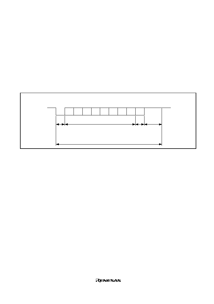
Rev. 2.0, 09/02, page 381 of 732
13.4
Operation in Asynchronous Mode
Figure 13.2 shows the general format for asynchronous serial communication. One frame consists
of a start bit (low level), followed by data, a parity bit, and finally stop bits (high level). In
asynchronous serial communication, the transmission line is usually held in the mark state (high
level). The SCI monitors the communication line, and when it goes to the space state (low level),
recognizes a start bit and starts serial communication. Inside the SCI, the transmitter and receiver
are independent units, enabling full-duplex communication. Both the transmitter and the receiver
also have a double-buffered structure, so that data can be read or written during transmission or
reception, enabling continuous data transfer.
LSB
Start
bit
MSB
Idle state
(mark state)
Stop bit
0
Transmit/receive data
D0
D1
D2
D3
D4
D5
D6
D7
0/1
1
1
1
1
Serial
data
Parity
bit
1 bit
1 or 2 bits
7 or 8 bits
1 bit
or
none
One unit of transfer data (character or frame)
Figure 13.2 Data Format in Asynchronous Communication (Example with 8-Bit Data,
Parity, Two Stop Bits)
Rev. 2.0, 09/02, page 382 of 732
13.4.1
Data Transfer Format
Table 13.8 shows the data transfer formats that can be used in asynchronous mode. Any of 12
transfer formats can be selected according to the SMR setting. For details on the multiprocessor
bit, refer to section 13.5, Multiprocessor Communication Function.
Table 13.8 Serial Transfer Formats (Asynchronous Mode)
PE
0
0
1
1
0
0
1
1
X
X
X
X
S
8-bit data
STOP
S
7-bit data
STOP
S
8-bit data
STOP STOP
S
8-bit data
P
STOP
S
7-bit data
STOP
P
S
8-bit data
MPB STOP
S
8-bit data
MPB STOP STOP
S
7-bit data
STOP
MPB
S
7-bit data
STOP
MPB
STOP
S
7-bit data
STOP
STOP
CHR
0
0
0
0
1
1
1
1
0
0
1
1
MP
0
0
0
0
0
0
0
0
1
1
1
1
STOP
0
1
0
1
0
1
0
1
0
1
0
1
SMR Settings
1
2
3
4
5
6
7
8
9
10
11
12
Serial Transfer Format and Frame Length
STOP
S
8-bit data
P STOP
S
7-bit data
STOP
P
STOP
Legend:
S: Start
bit
STOP: Stop bit
P: Parity
bit
MPB:
Multiprocessor bit
X: Don't care
Rev. 2.0, 09/02, page 383 of 732
13.4.2
Receive Data Sampling Timing and Reception Margin in Asynchronous Mode
In asynchronous mode, the SCI operates on a basic clock with a frequency of 16 times the bit rate.
In reception, the SCI samples the falling edge of the start bit using the basic clock, and performs
internal synchronization. Receive data is latched internally at the rising edge of the 8th pulse of the
basic clock as shown in figure 13.3. Thus the reception margin in asynchronous mode is given by
formula (1) below.
M = 0.5 ≠
1
2N
(D ≠ 0.5)
N
≠
≠ (L ≠ 0.5) F
100%
............................ Formula (1)
Where
M: Reception margin (
%
)
N: Ratio of bit rate to clock (N = 16)
D: Clock duty (D = 0 to 1.0)
L: Frame length (L = 9 to 12)
F: Absolute value of clock rate deviation
Assuming values of F = 0 and D = 0.5 in formula (1), a reception margin is given by formula
below.
M = {0.5 ≠ 1/(2
◊
16)}
◊
100 [%] = 46.875%
However, this is only the computed value, and a margin of 20% to 30% should be allowed in
system design.
Internal basic
clock
16 clocks
8 clocks
Receive data
(RxD)
Synchronization
sampling timing
Start bit
D0
D1
Data sampling
timing
15
0
7
15 0
0
7
Figure 13.3 Receive Data Sampling Timing in Asynchronous Mode
Rev. 2.0, 09/02, page 384 of 732
13.4.3
Clock
Either an internal clock generated by the on-chip baud rate generator or an external clock input at
the SCK pin can be selected as the SCI's serial clock, according to the setting of the C/A bit in
SMR and the CKE1 and CKE0 bits in SCR. When an external clock is input at the SCK pin, the
clock frequency should be 16 times the bit rate used.
When the SCI is operated on an internal clock, the clock can be output from the SCK pin. The
frequency of the clock output in this case is equal to the bit rate, and the phase is such that the
rising edge of the clock is in the middle of the transmit data, as shown in figure 13.4.
The clock must not be stopped during operation.
0
1 frame
D0
D1
D2
D3
D4
D5
D6
D7
0/1
1
1
SCK
TxD
Figure 13.4 Relation between Output Clock and Transmit Data Phase
(Asynchronous Mode)
Rev. 2.0, 09/02, page 385 of 732
13.4.4
SCI initialization (Asynchronous mode)
Before transmitting and receiving data, you should first clear the TE and RE bits in SCR to 0, then
initialize the SCI as described below. When the operating mode, transfer format, etc., is changed,
the TE and RE bits must be cleared to 0 before making the change using the following procedure.
When the TE bit is cleared to 0, the TDRE flag is set to 1. Note that clearing the RE bit to 0 does
not initialize the contents of the RDRF, PER, FER, and ORER flags, or the contents of RDR.
When the external clock is used in asynchronous mode, the clock must be supplied even during
initialization.
[1]
Start Initialization
Clear RIE, TIE, TEIE, MPIE, TE
and RE bits in SCR to 0
*
[2]
Yes
No
Set value in BRR
[3]
[4]
[5]
[6]
1-bit interval elapsed?
< Initialization completion>
[1] Set the clock selection in SCR.
[2] Set the data transfer format in SMR
and SDCR.
[3] Write a value corresponding to the
bit rate to BRR. Not necessary if an
external colck is used.
[4] Set the RIE, TIE, TEIE, and MPIE
bits in SCR.
[5] The PFC bits corresponding to the
external circuit to be used are
specified, so that the pin is RxD
input at data receive, and TxD
output at data transmission. In
addition, set the input/output to the
SCK according to the setting of
CKE1 and CKE0.
Not necessary to set the SCK pin
setting if CKE1 and CKE0 is set to
00 and asynchronous mode.
If the SCK pin setting is
synchronous clock output mode at
this time, then a clock starts being
output from the SCK pin.
[6] The TE and RE bits of SCR are set
to 1
*
. By doing this, the TxD, RxD,
and SCK pins can be used. When
transmitting, the TxD pin enters the
mark condition. When reception,
the RxD pin enters the idle state
wating for the start bit.
Set data transfer format in SMR
Set RIE, TIE, TEIE, and MPIE bits.
Set TE and RE bits in SCR to 1.
Set PFC for the pins to be used
(SCK, TXD, RXD)
Set CKE1 and CKE0 bits in SCR
(TE, RE bits are 0)
Note :
*
In simultaneous transmit/receive operation, the TE and RE bits must be cleared to 0 or set to 1
simultaneously.
Figure 13.5 Sample SCI Initialization Flowchart
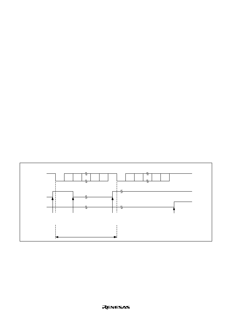
Rev. 2.0, 09/02, page 386 of 732
13.4.5
Data transmission (Asynchronous mode)
Figure 13.6 shows an example of the operation for transmission in asynchronous mode. In
transmission, the SCI operates as described below.
1. The SCI monitors the TDRE flag in SSR, and if is cleared to 0, recognizes that data has been
written to TDR, and transfers the data from TDR to TSR.
2. After transferring data from TDR to TSR, the SCI sets the TDRE flag to 1 and starts
transmission. If the TIE bit is set to 1 at this time, a transmit data empty interrupt request (TXI)
is generated. Because the TXI interrupt routine writes the next transmit data to TDR before
transmission of the current transmit data has finished, continuous transmission can be enabled.
3. Data is sent from the TxD pin in the following order: start bit, transmit data, parity bit or
multiprocessor bit (may be omitted depending on the format), and stop bit.
4. The SCI checks the TDRE flag at the timing for sending the stop bit.
5. If the TDRE flag is 0, the data is transferred from TDR to TSR, the stop bit is sent, and then
serial transmission of the next frame is started.
6. If the TDRE flag is 1, the TEND flag in SSR is set to 1, the stop bit is sent, and then the "mark
state" is entered in which 1 is output. If the TEIE bit in SCR is set to 1 at this time, a TEI
interrupt request is generated.
TDRE
TEND
0
1 frame
D0
D1
D7
0/1
1
0
D0
D1
D7
0/1
1
1
1
Data
Start
bit
Parity
bit
Stop
bit
Start
bit
Data
Parity
bit
Stop
bit
Data written to TDR
and TDRE flag cleared
to 0 in TXI interrupt
processing routine
TEI interrupt
request
generated
Idle state
(mark state)
TxD
TXI interrupt
request
generated
TXI interrupt
request
generated
Figure 13.6 Example of Operation in Transmission in Asynchronous Mode
(Example with 8-Bit Data, Parity, One Stop Bit)
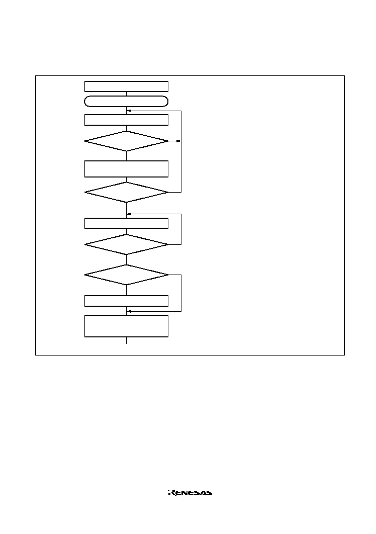
Rev. 2.0, 09/02, page 387 of 732
Figure 13.7 shows a sample flowchart for transmission in asynchronous mode.
No
<End>
[1]
Yes
Initialization
Start transmission
Read TDRE flag in SSR
[2]
No
Yes
No
Yes
Read TEND flag in SSR
[3]
No
Yes
[4]
Clear DR to 0
Clear TE bit in SCR to 0;
select the TxD pin
as an output port with the PFC
TDRE = 1
All data transmitted?
TEND = 1
Break output?
[1] SCI initialization:
Set the TxD pin using the PFC.
After the TE bit is set to 1, a frame
period of 1s is output, and
transmission is enabled. This action
doesn't initiate immediate data
transmission.
[2] SCI status check and transmit data
write:
Read SSR and check that the
TDRE flag is set to 1, then write
transmit data to TDR and clear the
TDRE flag to 0.
[3] Serial transmission continuation
procedure:
To continue serial transmission,
read 1 from the TDRE flag to
confirm that writing is possible, then
write data to TDR, and then clear
the TDRE flag to 0. Checking and
clearing of the TDRE flag is
automatic when the DMAC or DTC
is activated by a transmit data
empty interrupt (TXI) request, and
data is written to TDR.
[4] Break output at the end of serial
transmission:
To output a break in serial
transmission, first clear the port
data register (DR) to 0, then clear
the TE bit to 0 in SCR and use the
PFC to select the TxD pin as an
Write transmit data to TDR
and clear TDRE flag in SSR to 0
Figure 13.7 Sample Serial Transmission Flowchart
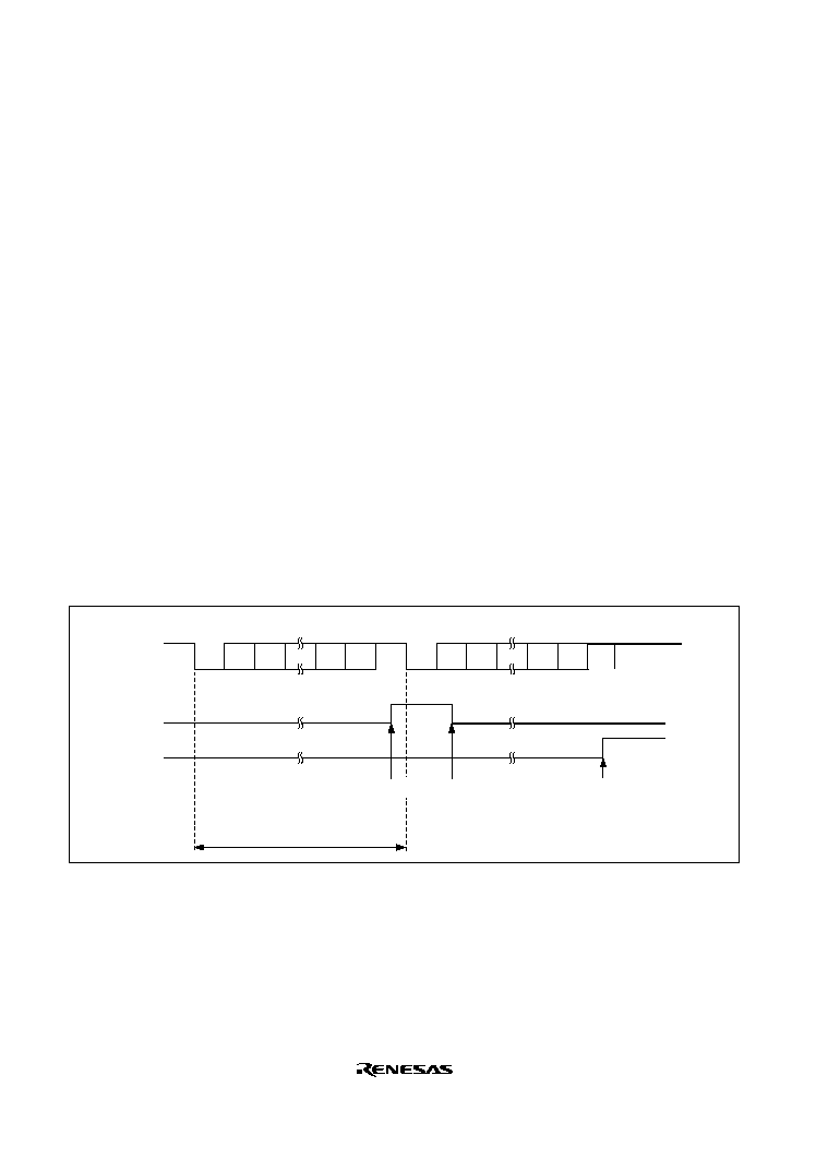
Rev. 2.0, 09/02, page 388 of 732
13.4.6
Serial data reception (Asynchronous mode)
Figure 13.8 shows an example of the operation for reception in asynchronous mode. In serial
reception, the SCI operates as described below.
1. The SCI monitors the communication line, and if a start bit is detected, performs internal
synchronization, receives receive data in RSR, and checks the parity bit and stop bit.
2. If an overrun error (when reception of the next data is completed while the RDRF flag is still
set to 1) occurs, the OER bit in SSR is set to 1. If the RIE bit in SCR is set to 1 at this time, an
ERI interrupt request is generated. Receive data is not transferred to RDR. The RDRF flag
remains to be set to 1.
3. If a parity error is detected, the PER bit in SSR is set to 1 and receive data is transferred to
RDR. If the RIE bit in SCR is set to 1 at this time, an ERI interrupt request is generated.
4. If a framing error (when the stop bit is 0) is detected, the FER bit in SSR is set to 1 and receive
data is transferred to RDR. If the RIE bit in SCR is set to 1 at this time, an ERI interrupt
request is generated.
5. If reception finishes successfully, the RDRF bit in SSR is set to 1, and receive data is
transferred to RDR. If the RIE bit in SCR is set to 1 at this time, an RXI interrupt request is
generated. Because the RXI interrupt processing routine reads the receive data transferred to
RDR before reception of the next receive data has finished, continuous reception can be
enabled.
RDRF
FER
0
1 frame
D0
D1
D7
0/1
1
0
D0
D1
D7
0/1
1
1
1
Data
Start
bit
Parity
bit
Stop
bit
Start
bit
Data
Parity
bit
Stop
bit
ERI interrupt
request generated
by framing error
Idle state
(mark state)
RDR data read and
RDRF flag cleared
to 0 in RXI interrupt
processing routine
RXI interrupt
request
generated
RxD
Figure 13.8 Example of SCI Operation in Reception
(Example with 8-Bit Data, Parity, One Stop Bit)

Rev. 2.0, 09/02, page 389 of 732
Table 13.9 shows the states of the SSR status flags and receive data handling when a receive error
is detected. If a receive error is detected, the RDRF flag retains its state before receiving data.
Reception cannot be resumed while a receive error flag is set to 1. Accordingly, clear the OER,
FER, PER, and RDRF bits to 0 before resuming reception. Figure 13.9 shows a sample flow chart
for serial data reception.
Table 13.9 SSR Status Flags and Receive Data Handling
SSR Status Flag
RDRF
*
OER
FER
PER
Receive Data
Receive Error Type
1
1
0
0
Lost
Overrun error
0
0
1
0
Transferred to RDR
Framing error
0
0
0
1
Transferred to RDR
Parity error
1
1
1
0
Lost
Overrun error + framing error
1
1
0
1
Lost
Overrun error + parity error
0
0
1
1
Transferred to RDR
Framing error + parity error
1
1
1
1
Lost
Overrun error + framing error +
parity error
Note:
*
The RDRF flag retains its state before data reception.
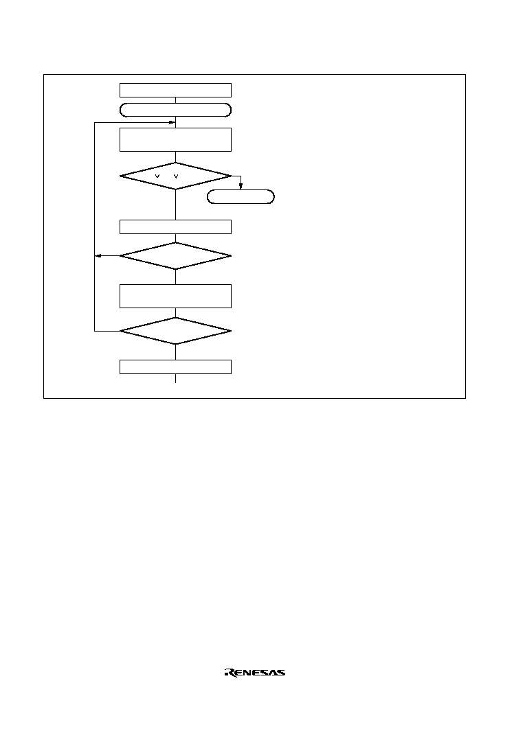
Rev. 2.0, 09/02, page 390 of 732
Yes
<End>
[1]
No
Initialization
Start reception
[2]
No
Yes
Read RDRF flag in SSR
[4]
[5]
Clear RE bit in SCR to 0
Read ORER, PER, and
FER flags in SSR
Error processing
(Continued on next page)
[3]
Read receive data in RDR, and
clear RDRF flag in SSR to 0
No
Yes
PER FER ORER = 1
RDRF = 1
All data received?
[1] SCI initialization:
Set the RxD pin using the PFC.
[2] [3] Receive error processing and break
detection:
If a receive error occurs, read the
ORER, PER, and FER flags in SSR to
identify the error. After performing the
appropriate error processing, ensure
that the ORER, PER, and FER flags are
all cleared to 0. Reception cannot be
resumed if any of these flags are set to
1. In the case of a framing error, a
break can be detected by reading the
value of the input port corresponding to
the RxD pin.
[4] SCI status check and receive data read:
Read SSR and check that RDRF = 1,
then read the receive data in RDR and
clear the RDRF flag to 0. Transition of
the RDRF flag from 0 to 1 can also be
identified by an RXI interrupt.
[5] Serial reception continuation procedure:
To continue serial reception, before the
stop bit for the current frame is
received, read the RDRF flag, read
RDR, and clear the RDRF flag to 0.
The RDRF flag is cleared automatically
when DMAC or DTC is activated by an
RXI interrupt and the RDR value is
read.
Figure 13.9 Sample Serial Reception Data Flowchart (1)

Rev. 2.0, 09/02, page 391 of 732
<End>
[3]
Error processing
Parity error processing
Yes
No
Clear ORER, PER, and
FER flags in SSR to 0
No
Yes
No
Yes
Framing error processing
No
Yes
Overrun error processing
ORER = 1
FER = 1
Break?
PER = 1
Clear RE bit in SCR to 0
Figure 13.9 Sample Serial Reception Data Flowchart (2)

Rev. 2.0, 09/02, page 392 of 732
13.5
Multiprocessor Communication Function
Use of the multiprocessor communication function enables data transfer to be performed among a
number of processors sharing communication lines by means of asynchronous serial
communication using the multiprocessor format, in which a multiprocessor bit is added to the
transfer data. When multiprocessor communication is carried out, each receiving station is
addressed by a unique ID code. The serial communication cycle consists of two component cycles:
an ID transmission cycle which specifies the receiving station, and a data transmission cycle. The
multiprocessor bit is used to differentiate between the ID transmission cycle and the data
transmission cycle. If the multiprocessor bit is 1, the cycle is an ID transmission cycle, and if the
multiprocessor bit is 0, the cycle is a data transmission cycle. Figure 13.10 shows an example of
inter-processor communication using the multiprocessor format. The transmitting station first
sends the ID code of the receiving station with which it wants to perform serial communication as
data with a 1 multiprocessor bit added. It then sends transmit data as data with a 0 multiprocessor
bit added. The receiving station skips data until data with a 1 multiprocessor bit is sent. When data
with a 1 multiprocessor bit is received, the receiving station compares that data with its own ID.
The station whose ID matches then receives the data sent next. Stations whose ID does not match
continue to skip data until data with a 1 multiprocessor bit is again received.
The SCI uses the MPIE bit in SCR to implement this function. When the MPIE bit is set to 1,
transfer of receive data from RSR to RDR, error flag detection, and setting the SSR status flags,
RDRF, FER, and OER to 1 are inhibited until data with a 1 multiprocessor bit is received. On
reception of receive character with a 1 multiprocessor bit, the MPBR bit in SSR is set to 1 and the
MPIE bit is automatically cleared, thus normal reception is resumed. If the RIE bit in SCR is set to
1 at this time, an RXI interrupt is generated.
When the multiprocessor format is selected, the parity bit setting is invalid. All other bit settings
are the same as those in normal asynchronous mode. The clock used for multiprocessor
communication is the same as that in normal asynchronous mode.

Rev. 2.0, 09/02, page 393 of 732
Transmitting
station
Receiving
station A
(ID = 01)
Receiving
station B
(ID = 02)
Receiving
station C
(ID = 03)
Receiving
station D
(ID = 04)
Serial transmission line
Serial
data
ID transmission cycle =
receiving station
specification
Data transmission cycle =
Data transmission to
receiving station specified
by ID
(MPB = 1)
(MPB = 0)
H'01
H'AA
Legend:
MPB: Multiprocessor bit
Figure 13.10 Example of Communication Using Multiprocessor Format
(Transmission of Data H'AA to Receiving Station A)
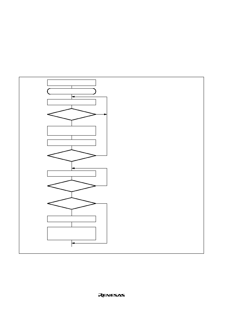
Rev. 2.0, 09/02, page 394 of 732
13.5.1
Multiprocessor Serial Data Transmission
Figure 13.11 shows a sample flowchart for multiprocessor serial data transmission. For an ID
transmission cycle, set the MPBT bit in SSR to 1 before transmission. For a data transmission
cycle, clear the MPBT bit in SSR to 0 before transmission. All other SCI operations are the same
as those in asynchronous mode.
No
<End>
[1]
Yes
Initialization
Start transmission
Read TDRE flag in SSR
[2]
No
Yes
No
Yes
Read TEND flag in SSR
[3]
No
Yes
[4]
Clear DR to 0
Clear TE bit in SCR to 0;
select the TxD pin
as an output port with the PFC
TDRE = 1
All data transmitted?
TEND = 1
Break output?
Clear TDRE flag to 0
[1] SCI initialization:
Set the TxD pin using the PFC.
After the TE bit is set to 1, a
frame period of 1s is output, and
transmission is enabled. This
action doesn't initiate immediate
data transmission.
[2] SCI status check and transmit
data write:
Read SSR and check that the
TDRE flag is set to 1, then write
transmit data to TDR. Set the
MPBT bit in SSR to 0 or 1.
Finally, clear the TDRE flag to 0.
[3] Serial transmission continuation
procedure:
To continue serial transmission,
be sure to read 1 from the TDRE
flag to confirm that writing is
possible, then write data to TDR,
and then clear the TDRE flag to
0. Checking and clearing of the
TDRE flag is automatic when the
DMAC or DTC is activated by a
transmit data empty interrupt
(TXI) request, and data is written
to TDR.
[4] Break output at the end of serial
transmission:
To output a break in serial
transmission, first clear the port
data register (DR) to 0, then
clear the TE bit to 0 in SCR and
Write transmit data to TDR and
set MPBT bit in SSR
Figure 13.11 Sample Multiprocessor Serial Transmission Flowchart
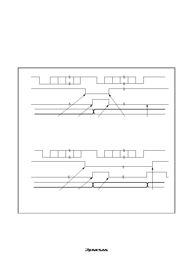
Rev. 2.0, 09/02, page 395 of 732
13.5.2
Multiprocessor Serial Data Reception
Figure 13.13 shows a sample flowchart for multiprocessor serial data reception. If the MPIE bit in
SCR is set to 1, data is skipped until data with a 1 multiprocessor bit is sent. On receiving data
with a 1 multiprocessor bit, the receive data is transferred to RDR. An RXI interrupt request is
generated at this time. All other SCI operations are the same as in asynchronous mode. Figure
13.12 shows an example of SCI operation for multiprocessor format reception.
MPIE
RxD
RxD
RDR
value
0
D0
D1
D7
1
1
0
D0
D1
D7
0
1
1
1
Data (ID1)
Start
bit
MPB
Stop
bit
Start
bit
Data (Data1)
MPB
Stop
bit
Data (ID2)
Start
bit
Stop
bit
Start
bit
Data (Data2)
Stop
bit
RXI interrupt
request
(multiprocessor
interrupt)
generated
Idle state
(mark state)
RDRF
RDR data read
and RDRF flag
cleared to 0 in
RXI interrupt
processing routine
If not this station's ID,
MPIE bit is set to 1
again
RXI interrupt request is
not generated, and RDR
retains its state
ID1
(a) Data does not match station's ID
MPIE
RDR
value
0
D0
D1
D7
1
1
0
D0
D1
D7
0
1
1
1
MPB
MPB
RXI interrupt
request
(multiprocessor
interrupt)
generated
Idle state
(mark state)
RDRF
RDR data read and
RDRF flag cleared
to 0 in RXI interrupt
processing routine
Matches this station's ID,
so reception continues,
and data is received in RXI
interrupt processing routine
MPIE bit is set to 1
again
ID2
(b) Data matches station's ID
Data2
ID1
MPIE = 0
MPIE = 0
Figure 13.12 Example of SCI Operation in Reception
(Example with 8-Bit Data, Multiprocessor Bit, One Stop Bit)
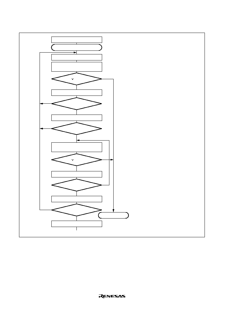
Rev. 2.0, 09/02, page 396 of 732
Yes
<End>
[1]
No
Initialization
Start reception
No
Yes
[4]
Clear RE bit in SCR to 0
Error processing
(Continued on
next page)
[5]
No
Yes
FER ORER = 1
RDRF = 1
All data received?
Set MPIE bit in SCR to 1
[2]
Read ORER and FER flags
in SSR
Read RDRF flag in SSR
[3]
Read receive data in RDR
No
Yes
This station's ID?
Read ORER and FER flags
in SSR
Yes
No
Read RDRF flag in SSR
No
Yes
FER ORER = 1
Read receive data in RDR
RDRF = 1
[1] SCI initialization:
Set the RxD pin using the PFC.
[2] ID reception cycle:
Set the MPIE bit in SCR to 1.
[3] SCI status check, ID reception and
comparison:
Read SSR and check that the RDRF
flag is set to 1, then read the receive
data in RDR and compare it with this
station's ID.
If the data is not this station's ID, set the
MPIE bit to 1 again, and clear the RDRF
flag to 0.
If the data is this station's ID, clear the
RDRF flag to 0.
[4] SCI status check and data reception:
Read SSR and check that the RDRF
flag is set to 1, then read the data in
RDR.
[5] Receive error processing and break
detection:
If a receive error occurs, read the ORER
and FER flags in SSR to identify the
error. After performing the appropriate
error processing, ensure that the ORER
and FER flags are all cleared to 0.
Reception cannot be resumed if either
of these flags is set to 1.
In the case of a framing error, a break
can be detected by reading the RxD pin
value.
Figure 13.13 Sample Multiprocessor Serial Reception Flowchart (1)
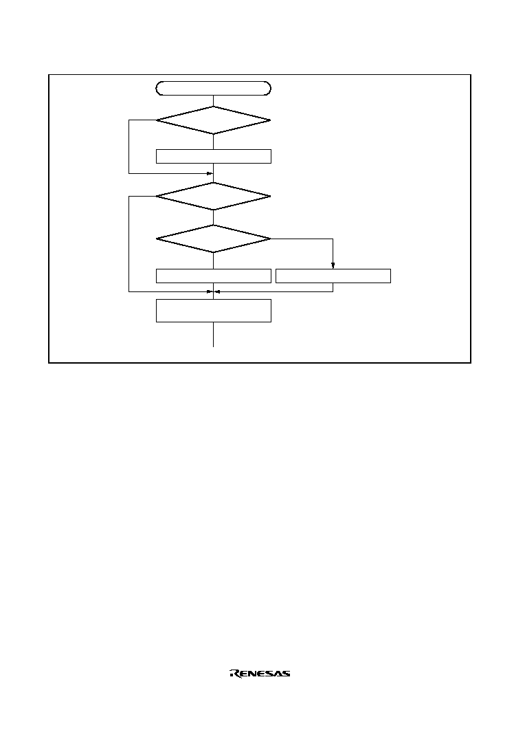
Rev. 2.0, 09/02, page 397 of 732
<End>
Error processing
Yes
No
Clear ORER and
FER flags in SSR to 0
No
Yes
No
Yes
Framing error processing
Overrun error processing
ORER = 1
FER = 1
Break?
Clear RE bit in SCR to 0
[5]
Figure 13.13 Sample Multiprocessor Serial Reception Flowchart (2)
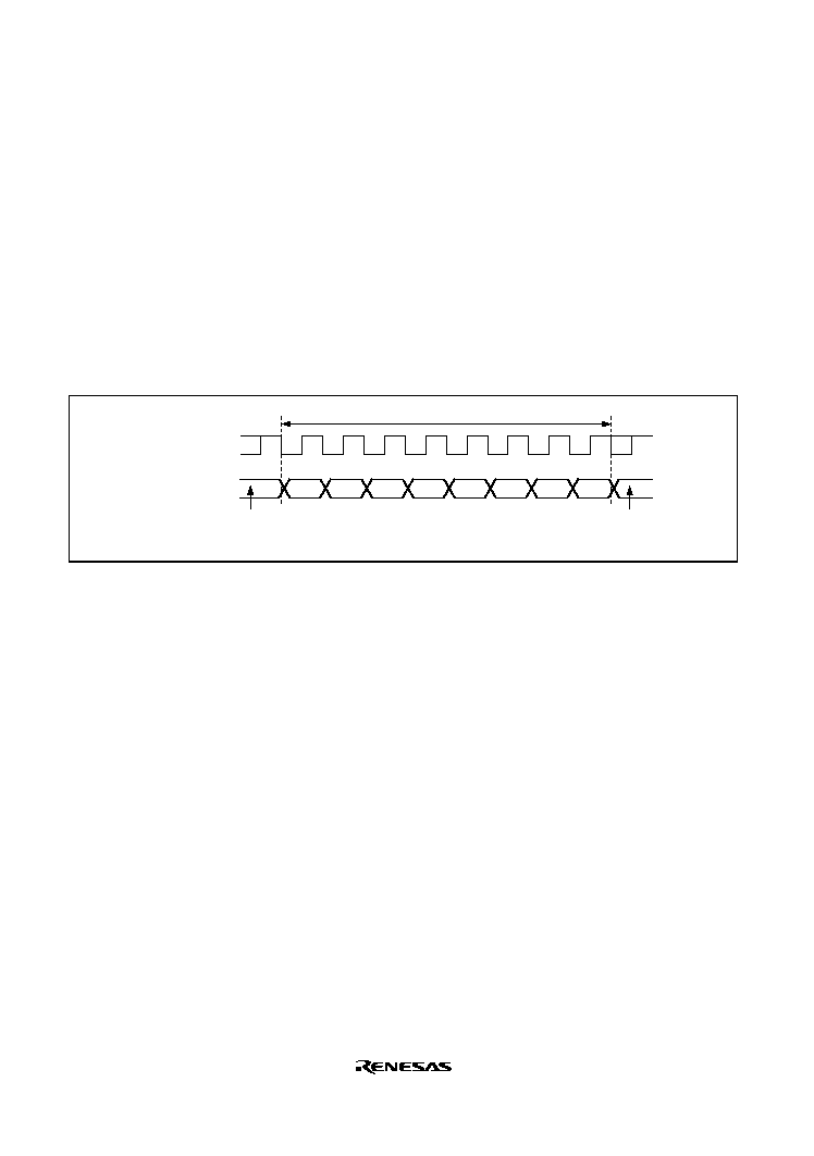
Rev. 2.0, 09/02, page 398 of 732
13.6
Operation in Clocked Synchronous Mode
Figure 13.14 shows the general format for clocked synchronous communication. In clocked
synchronous mode, data is transmitted or received in synchronization with clock pulses. Data is
transferred in 8-bit units. In clocked synchronous serial communication, data on the transmission
line is output from one falling edge of the serial clock to the next. In clocked synchronous mode,
the SCI receives data in synchronization with the rising edge of the serial clock. After 8-bit data is
output, the transmission line holds the MSB state. In clocked synchronous mode, no parity or
multiprocessor bit is added. Inside the SCI, the transmitter and receiver are independent units,
enabling full-duplex communication by use of a common clock. Both the transmitter and the
receiver also have a double-buffered structure, so that data can be read or written during
transmission or reception, enabling continuous data transfer.
Don't care
Don't care
One unit of transfer data (character or frame)
Bit 0
Serial data
Synchronization
clock
Bit 1
Bit 3
Bit 4
Bit 5
LSB
MSB
Bit 2
Bit 6
Bit 7
*
*
Note:
*
High except in continuous transfer
Figure 13.14 Data Format in Clocked Synchronous Communication (For LSB-First)
13.6.1
Clock
Either an internal clock generated by the on-chip baud rate generator or an external
synchronization clock input at the SCK pin can be selected, according to the setting of CKE1 and
CKE0 bits in SCR. When the SCI is operated on an internal clock, the serial clock is output from
the SCK pin. Eight serial clock pulses are output in the transfer of one character, and when no
transfer is performed, the clock is fixed high.
13.6.2
SCI initialization (Clocked Synchronous mode)
Before transmitting and receiving data, you should first clear the TE and RE bits in SCR to 0, then
initialize the SCI as described in a sample flowchart in figure 13.15. When the operating mode,
transfer format, etc., is changed, the TE and RE bits must be cleared to 0 before making the
change using the following procedure. When the TE bit is cleared to 0, the TDRE flag is set to 1.
Note that clearing the RE bit to 0 does not change the contents of the RDRF, PER, FER, and
ORER flags, or the contents of RDR.
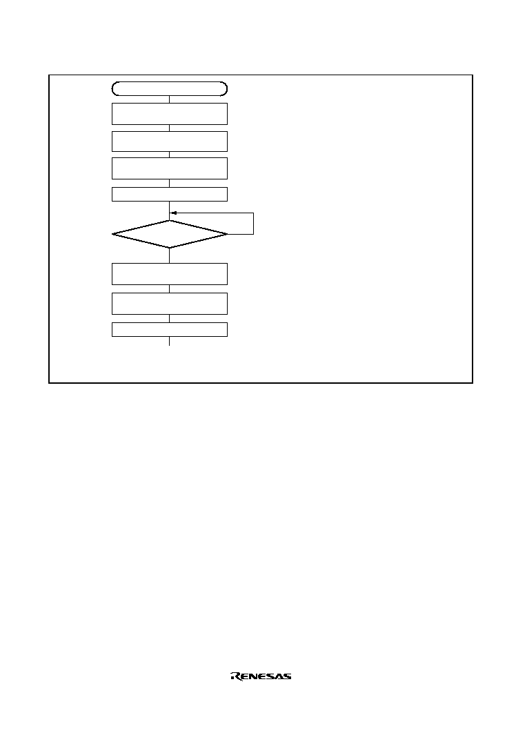
Rev. 2.0, 09/02, page 399 of 732
Wait
<Transfer start>
Start initialization
Set data transfer format in
SMR to 0.
Set RIE, TIE, TEIE, and MPIE
bits in SCR.
Set PFC to the external pins
(SCK, TXD, and RXD) to be used.
No
Yes
Set value in BRR
Set TE or RE bits in SCR to 1.
Clear RIE, TIE, TEIE, MPIE, TE
and RE bits in SCR to 0.
*
[2]
[3]
[4]
[5]
[6]
1-bit interval elapsed?
Set CKE1 and CKE0 bits in
SCR to 0. ( TE and RE bits are 0)
[1]
[1] Set the clock selection in SCR.
[2] Set the data transfer format in SMR.
[3] Write a value corresponding to the bit
rate to BRR. Not necessary if an
external clock is used.
[4] Set RIE, TIE, TEIE, and MPIE bits in
SCR to 1.
[5] Set PFC for the external pins to be
used. Set RXD input for reception and
TXD output for transmission. Set SCK
input/output according to the value set
by CKE1 and CKE0.
[6] Set TE or RE bit in SCR to 1
*
. Then,
TXD, RXD, and SCK pins can be used.
The TXD pin is in the mark status at
transmission. If the setting is reception
in clocked synchronous mode and
synchronous clock output (clock
master) at this time, then a clock starts
being output from the SCK pins.
Note: In simultaneous transmit and receive operation, the TE and RE bits should both be
cleared to 0 or set to 1 simultaneously.
Figure 13.15 Sample SCI Initialization Flowchart
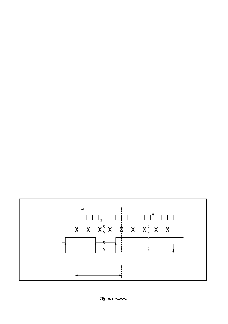
Rev. 2.0, 09/02, page 400 of 732
13.6.3
Serial data transmission (Clocked Synchronous mode)
Figure 13.16 shows an example of SCI operation for transmission in clocked synchronous mode.
In serial transmission, the SCI operates as described below.
1. The SCI monitors the TDRE flag in SSR, and if is 0, recognizes that data has been written to
TDR, and transfers the data from TDR to TSR.
2. After transferring data from TDR to TSR, the SCI sets the TDRE flag to 1 and starts
transmission. If the TIE bit in SCR is set to 1 at this time, a transmit data empty (TXI) interrupt
request is generated. Because the TXI interrupt routine writes the next transmit data to TDR
before transmission of the current transmit data has finished, continuous transmission can be
enabled.
3. 8-bit data is sent from the TxD pin synchronized with the output clock when output clock
mode has been specified and synchronized with the input clock when use of an external clock
has been specified.
4. The SCI checks the TDRE flag at the timing for sending the MSB (bit 7).
5. If the TDRE flag is cleared to 0, data is transferred from TDR to TSR, and serial transmission
of the next frame is started.
6. If the TDRE flag is set to 1, the TEND flag in SSR is set to 1, and the TxD pin maintains the
output state of the last bit. If the TEIE bit in SCR is set to 1 at this time, a TEI interrupt request
is generated. The SCK pin is fixed high.
Figure 13.17 shows a sample flowchart for serial data transmission. Even if the TDRE flag is
cleared to 0, transmission will not start while a receive error flag (ORER, FER, or PER) is set to 1.
Make sure to clear the receive error flags to 0 before starting transmission. Note that clearing the
RE bit to 0 does not clear the receive error flags.
Transfer
direction
Bit 0
Serial data
Synchroniza-
tion clock
1 frame
TDRE
TEND
Bit 1
Bit 7
Bit 0
Bit 1
Bit 6
Bit 7
TXI interrupt
request
generated
Data written to TDR
and TDRE flag cleared
to 0 in TXI interrupt
processing routine
TEI interrupt
request
generated
TXI interrupt
request
generated
Figure 13.16 Sample SCI Transmission Operation in Clocked Synchronous Mode
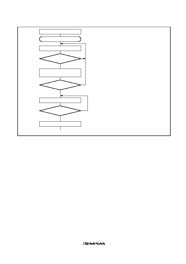
Rev. 2.0, 09/02, page 401 of 732
No
<End>
[1]
Yes
Initialization
Start transmission
Read TDRE flag in SSR
[2]
Write transmit data to TDR and
clear TDRE flag in SSR to 0
No
Yes
No
Yes
Read TEND flag in SSR
[3]
Clear TE bit in SCR to 0
TDRE = 1
All data transmitted?
TEND = 1
[1] SCI initialization:
Set the TxD pin using the PFC.
[2] SCI status check and transmit data
write:
Read SSR and check that the TDRE
flag is set to 1, then write transmit data
to TDR and clear the TDRE flag to 0.
[3] Serial transmission continuation
procedure:
To continue serial transmission, be
sure to read 1 from the TDRE flag to
confirm that writing is possible, then
write data to TDR, and then clear the
TDRE flag to 0.
Checking and clearing of the TDRE
flag is automatic when the DMAC or
DTC is activated by a transmit data
empty interrupt (TXI) request and data
is written to TDR.
Figure 13.17 Sample Serial Transmission Flowchart
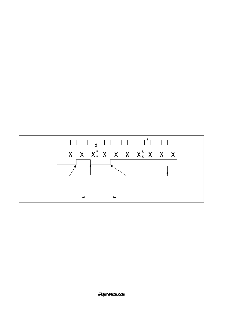
Rev. 2.0, 09/02, page 402 of 732
13.6.4
Serial data reception (Clocked Synchronous mode)
Figure 13.18 shows an example of SCI operation for reception in clocked synchronous mode. In
serial reception, the SCI operates as described below.
1. The SCI performs internal initialization in synchronization with a synchronization clock input
or output, starts receiving data, and stores the received data in RSR.
2. If an overrun error (when reception of the next data is completed while the RDRF flag is still
set to 1) occurs, the ORER bit in SSR is set to 1. If the RIE bit in SCR is set to 1 at this time,
an ERI interrupt request is generated. Receive data is not transferred to RDR. The RDRF flag
remains to be set to 1.
3. If reception finishes successfully, the RDRF bit in SSR is set to 1, and receive data is
transferred to RDR. If the RIE bit in SCR is set to 1 at this time, an RXI interrupt request is
generated. Because the RXI interrupt processing routine reads the receive data transferred to
RDR before reception of the next receive data has finished, continuous reception can be
enabled.
Bit 7
Serial data
Synchroniza-
tion clock
1 frame
RDRF
ORER
Bit 0
Bit 7
Bit 0
Bit 1
Bit 6
Bit 7
RXI interrupt
request
generated
RDR data read and
RDRF flag cleared
to 0 in RXI interrupt
processing routine
ERI interrupt
request generated
by overrun error
RXI interrupt
request
generated
Figure 13.18 Example of SCI Operation in Reception
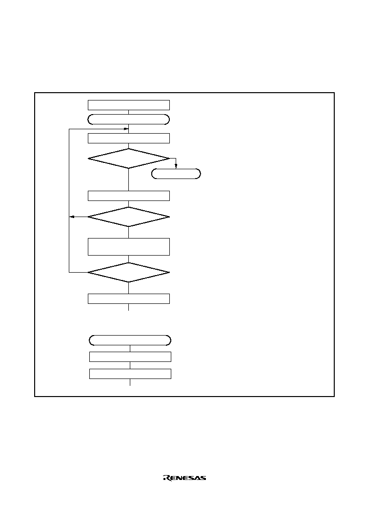
Rev. 2.0, 09/02, page 403 of 732
Reception cannot be resumed while a receive error flag is set to 1. Accordingly, clear the ORER,
FER, PER, and RDRF bits to 0 before resuming reception. Figure 13.19 shows a sample flowchart
for serial data reception.
Yes
<End>
[1]
No
Initialization
Start reception
[2]
No
Yes
Read RDRF flag in SSR
[4]
[5]
Clear RE bit in SCR to 0
Error processing
(Continued below)
[3]
Read receive data in RDR, and
clear RDRF flag in SSR to 0
No
Yes
ORER = 1
RDRF = 1
All data received?
Read ORER flag in SSR
<End>
Error processing
Overrun error processing
Clear ORER flag in SSR to 0
[3]
[1] SCI initialization:
Set the RxD pin using the PFC.
[2] [3] Receive error processing:
If a receive error occurs, read the
ORER flag in SSR, and after
performing the appropriate error
processing, clear the ORER flag to 0.
Transfer cannot be resumed if the
ORER flag is set to 1.
[4] SCI status check and receive data
read:
Read SSR and check that the RDRF
flag is set to 1, then read the receive
data in RDR and clear the RDRF flag
to 0.
Transition of the RDRF flag from 0 to 1
can also be identified by an RXI
interrupt.
[5] Serial reception continuation
procedure:
To continue serial reception, before
the MSB (bit 7) of the current frame is
received, reading the RDRF flag,
reading RDR, and clearing the RDRF
flag to 0 should be finished. The
RDRF flag is cleared automatically
when the DMAC or DTC is activated
by a receive data full interrupt (RXI)
request and the RDR value is read.
Figure 13.19 Sample Serial Reception Flowchart

Rev. 2.0, 09/02, page 404 of 732
13.6.5
Simultaneous Serial Data Transmission and Reception (Clocked Synchronous
mode)
Figure 13.20 shows a sample flowchart for simultaneous serial transmit and receive operations.
The following procedure should be used for simultaneous serial data transmit and receive
operations after the SCI initialization. To switch from transmit mode to simultaneous transmit and
receive mode, after checking that the SCI has finished transmission and the TDRE and TEND
flags are set to 1, clear TE to 0. Then simultaneously set TE and RE to 1 with a single instruction.
To switch from receive mode to simultaneous transmit and receive mode, after checking that the
SCI has finished reception, clear RE to 0. Then after checking that the RDRF and receive error
flags (ORER, FER, and PER) are cleared to 0, simultaneously set TE and RE to 1 with a single
instruction.
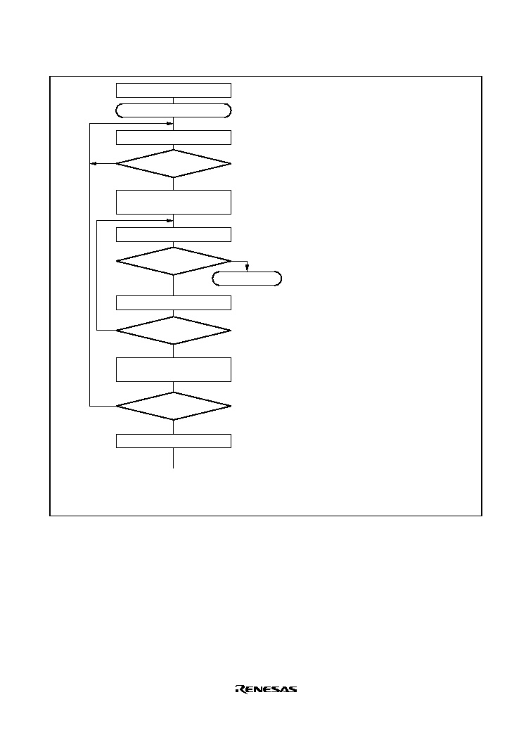
Rev. 2.0, 09/02, page 405 of 732
Yes
<End>
[1]
No
Initialization
Start transmission/reception
[5]
Error processing
[3]
No
Yes
ORER = 1
All data received?
[2]
Read TDRE flag in SSR
No
Yes
TDRE = 1
Write transmit data to TDR and
clear TDRE flag in SSR to 0
No
Yes
RDRF = 1
Read ORER flag in SSR
[4]
Read RDRF flag in SSR
[1] SCI initialization:
Set the TxD and RxD pins using the PFC.
[2] SCI status check and transmit data write:
Read SSR and check that the TDRE flag
is set to 1, then write transmit data to
TDR and clear the TDRE flag to 0.
Transition of the TDRE flag from 0 to 1
can also be identified by a TXI interrupt.
[3] Receive error processing:
If a receive error occurs, read the ORER
flag in SSR, and after performing the
appropriate error processing, clear the
ORER flag to 0. Transmission/reception
cannot be resumed if the ORER flag is
set to 1.
[4] SCI status check and receive data read:
Read SSR and check that the RDRF flag
is set to 1, then read the receive data in
RDR and clear the RDRF flag to 0.
Transition of the RDRF flag from 0 to 1
can also be identified by an RXI interrupt.
[5] Serial transmission/reception continuation
procedure:
To continue serial transmission/
reception, before the MSB (bit 7) of the
current frame is received, finish reading
the RDRF flag, reading RDR, and
clearing the RDRF flag to 0. Also, before
the MSB (bit 7) of the current frame is
transmitted, read 1 from the TDRE flag to
confirm that writing is possible. Then
write data to TDR and clear the TDRE
flag to 0.
Checking and clearing of the TDRE flag is
automatic when the DMAC or DTC is
activated by a transmit data empty
interrupt (TXI) request and data is written
to TDR. Also, the RDRF flag is cleared
automatically when the DMAC or DTC is
activated by a receive data full interrupt
(RXI) request and the RDR value is read.
Note: When switching from transmit or receive operation to simultaneous transmit and receive operations,
first clear the TE bit and RE bit to 0, then set both these bits to 1 simultaneously.
Clear TE and RE bits in SCR to 0
Read receive data in RDR, and
clear RDRF flag in SSR to 0
Figure 13.20 Sample Flowchart of Simultaneous Serial Transmit and Receive Operations

Rev. 2.0, 09/02, page 406 of 732
13.7
Interrupt Sources
13.7.1
Interrupts in Normal Serial Communication Interface Mode
Table 13.10 shows the interrupt sources in normal serial communication interface mode. A
different interrupt vector is assigned to each interrupt source, and individual interrupt sources can
be enabled or disabled using the enable bits in SCR.
When the TDRE flag in SSR is set to 1, a TXI interrupt request is generated. When the TEND flag
in SSR is set to 1, a TEI interrupt request is generated. A TXI interrupt request can activate the
DMAC or DTC to perform data transfer. The TDRE flag is cleared to 0 automatically when data
transfer is performed by the DMAC or DTC.
When the RDRF flag in SSR is set to 1, an RXI interrupt request is generated. When the ORER,
PER, or FER flag in SSR is set to 1, an ERI interrupt request is generated. An RXI interrupt
request can activate the DMAC or DTC to perform data transfer. The RDRF flag is cleared to 0
automatically when data transfer is performed by the DMAC or DTC.
A TEI interrupt is generated when the TEND flag is set to 1 while the TEIE bit is set to 1. If a TEI
interrupt and a TXI interrupt are generated simultaneously, the TXI interrupt has priority for
acceptance. However, note that if the TDRE and TEND flags are cleared simultaneously by the
TXI interrupt routine, the SCI cannot branch to the TEI interrupt routine later.

Rev. 2.0, 09/02, page 407 of 732
Table 13.10 SCI Interrupt Sources
Channel
Name
Interrupt Source
Interrupt Flag
DMAC or DTC
Activation
ERI_0
Receive Error
ORER, FER, PER
Not possible
RXI_0
Receive Data Full
RDRF
Possible
TXI_0
Transmit Data Empty
TDRE
Possible
0
TEI_0
Transmission End
TEND
Not possible
ERI_1
Receive Error
ORER, FER, PER
Not possible
RXI_1
Receive Data Full
RDRF
Possible
TXI_1
Transmit Data Empty
TDRE
Possible
1
TEI_1
Transmission End
TEND
Not possible
ERI_2
Receive Error
ORER, FER, PER
Not possible
RXI_2
Receive Data Full
RDRF
Possible
TXI_2
Transmit Data Empty
TDRE
Possible
2
TEI_2
Transmission End
TEND
Not possible
ERI_3
Receive Error
ORER, FER, PER
Not possible
RXI_3
Receive Data Full
RDRF
Possible
TXI_3
Transmit Data Empty
TDRE
Possible
3
TEI_3
Transmission End
TEND
Not possible

Rev. 2.0, 09/02, page 408 of 732
13.8
Usage Notes
13.8.1
TDR Write and TDRE Flag
The TDRE bit in the serial status register (SSR) is a status flag indicating transferring of transmit
data from TDR into TSR. The SCI sets the TDRE bit to 1 when it transfers data from TDR to
TSR.
Data can be written to TDR regardless of the TDRE bit status.
If new data is written in TDR when TDRE is 0, however, the old data stored in TDR will be lost
because the data has not yet been transferred to TSR. Before writing transmit data to TDR, be sure
to check that the TDRE bit is set to 1.
13.8.2
Module Standby Mode Setting
SCI operation can be disabled or enabled using the module standby control register. The initial
setting is for SCI operation to be halted. Register access is enabled by clearing module standby
mode. For details, refer to section 24, Power-Down modes.
13.8.3
Break Detection and Processing (Asynchronous Mode Only)
When framing error detection is performed, a break can be detected by reading the RxD pin value
directly. In a break, the input from the RxD pin becomes all 0s, and so the FER flag is set, and the
PER flag may also be set. Note that, since the SCI continues the receive operation after receiving a
break, even if the FER flag is cleared to 0, it will be set to 1 again.
13.8.4
Sending a Break Signal (Asynchronous Mode Only)
The TxD pin becomes of the I/O port general I/O pin with the I/O direction and level determined
by the port data register (DR) and the port I/O register (IOR) of the pin function controller (PFC).
These conditions allow break signals to be sent.
The DR value is substituted for the marking status until the PFC is set. Consequently, the output
port is set to initially output a 1.
To send a break in serial transmission, first clear the DR to 0, then establish the TxD pin as an
output port using the PFC.
When the TE bit is cleared to 0, the transmission section is initialized regardless of the present
transmission status.
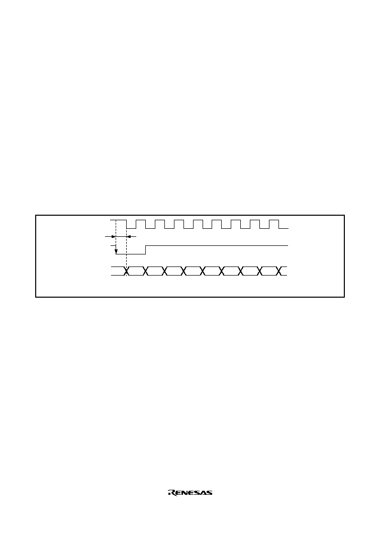
Rev. 2.0, 09/02, page 409 of 732
13.8.5
Receive Error Flags and Transmit Operations (Clocked Synchronous Mode Only)
Transmission cannot be started when a receive error flag (ORER, PER, or FER) is set to 1, even if
the TDRE flag is cleared to 0. Be sure to clear the receive error flags to 0 before starting
transmission. Note also that receive error flags cannot be cleared to 0 even if the RE bit is cleared
to 0.
13.8.6
Constraints on DMAC and DTC Use
1. When using an external clock source for the serial clock, update TDR with the DMAC or the
DTC, and then after the elapse of five peripheral clocks (P
) or more, input a transmit clock. If
a transmit clock is input in the first four P
clocks after TDR is written, an error may occur
(figure 13.21).
2. Before reading the receive data register (RDR) with the DMAC or the DTC, select the receive-
data-full (RXI) interrupt of the SCI as a start-up source.
D0
SCK
TDRE
D1
D2
D3
D4
D5
D6
D7
t
Note: During external clock operation, an error may occur if t is 4 P
clocks or less.
Figure 13.21 Example of Clocked Synchronous Transmission with DMAC/DTC
13.8.7
Cautions on Clocked Synchronous External Clock Mode
1. Set TE = RE = 1 only when external clock SCK is 1.
2. Do not set TE = RE = 1 until at least four P
clocks after external clock SCK has changed
from 0 to 1.
3. When receiving, RDRF is 1 when RE is cleared to 0 after 2.5 to 3.5 P
clocks from the rising
edge of the RxD D7 bit SCK input, but copying to RDR is not possible.
13.8.8
Caution on Clocked Synchronous Internal Clock Mode
When receiving, RDRF is 1 when RE is cleared to 0 after 1.5 P
clocks from the rising edge of the
RxD D7 bit SCK output, but copying to RDR is not possible.

Rev. 2.0, 09/02, page 410 of 732

IFIIC20A_010020020700
Rev. 2.0, 09/02, page 411 of 732
Section 14 I
2
C Bus Interface (IIC) Option
The I
2
C bus interface is an optional feature. When using this optional feature, pay attention to the
following points:
1. A "W" is added to the product-type name of a mask-ROM product which includes an
optional feature.
2
For the F-ZTAT version, the product-type code is the same regardless of whether or not
this feature is included. When you wish to use this optional feature, please contact
Hitachi
s sales office.
This LSI incorporates a single-channel I
2
C bus interface. The I
2
C bus interface complies with the
I
2
C bus (Inter-IC Bus) communications protocol that is advocated by Philips Co. and implements a
subset of the specification of that protocol. Note, however, that the configuration of the registers
that control the I
2
C bus differs on some points from that of Phillips'.
Data transfer is carried out by the data line (SDA0) and clock line (SCL0). This makes the
interface efficient in terms of the use of area for connectors and printed circuits.
14.1
Features
∑
Selection of addressing or non-addressing format
I
2
C bus format: addressing format with an acknowledge bit, master and slave operation
Serial format: non-addressing format without an acknowledge bit, and with master operation
only
∑
This I
2
C bus format complies with the I
2
C bus interface advocated by Phillips.
∑
In the I
2
C bus format, two slave addresses are specifiable for a single device.
∑
Automatic creation of start and stop conditions in slave-mode of the I
2
C bus format
∑
Selectable acknowledge output level during reception in the I
2
C bus format
∑
Automatic loading of the acknowledge bit is available during transmission in the I
2
C bus
format.
∑
A wait function is available in the I
2
C bus format in the master mode.
After all data other than the acknowledge bit has been transferred, the system can be placed in
the wait state by setting SCL0 low.
∑
A wait function for the slave mode is available in the I
2
C bus format.
After all data other than the acknowledge bit has been transferred, a request to enter the wait
state can be issued by setting SCL0 low.
∑
Three interrupt sources: (ICI) completion of data transfer, address matching, or detection of the
stop condition
∑
16 variants of the internal clock are selectable in the master mode.
∑
Automatic transfer of the register data is enabled by activating the DTC.
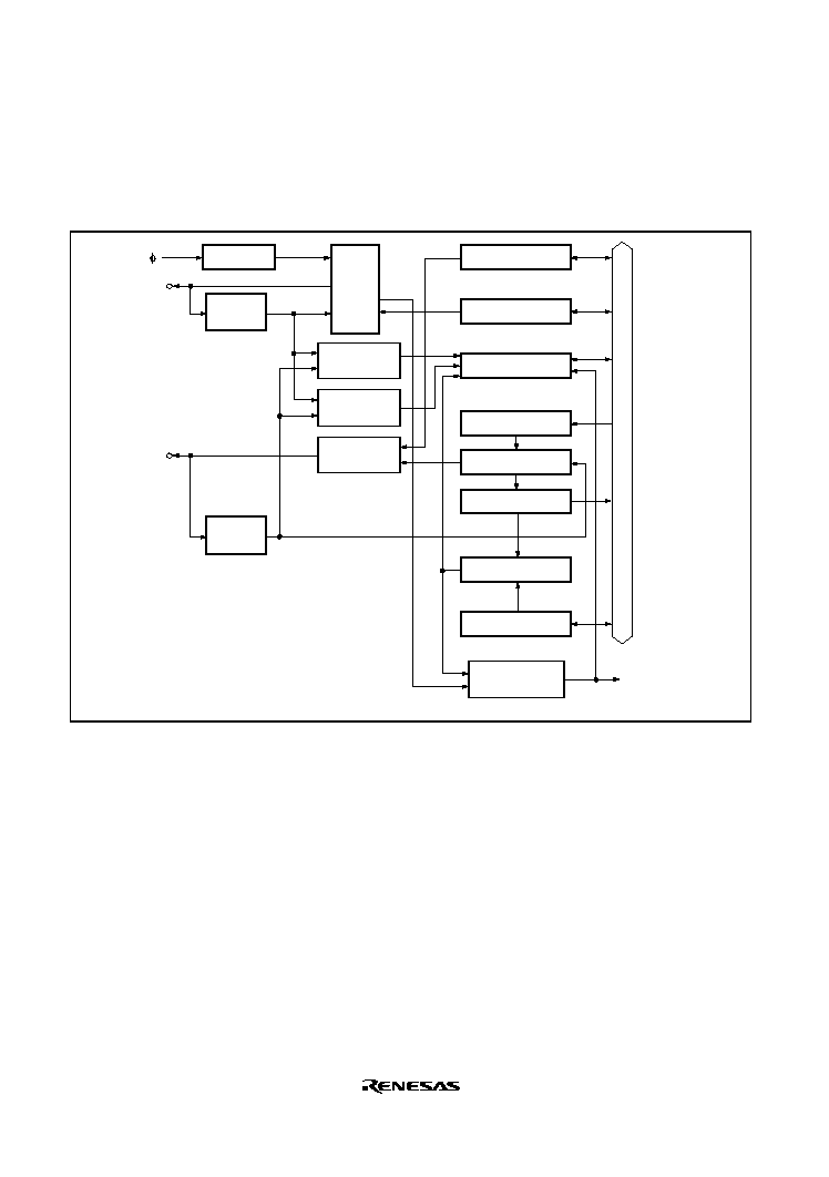
Rev. 2.0, 09/02, page 412 of 732
Figure 14.1 is a block diagram of the I
2
C bus interface. Figure 14.2 shows an example of the
connection of I
2
C bus interfaces. Since the I/O pins are driven only by the NMOS transistor, they
operate in the same way as pins driven by an open-drain NMOS transistor. The voltage that can be
applied to the I/O pins depends on the supply voltage (V
CC
) of the LSI.
SCL0
ICCR
ICMR
ICSR
ICDRS
SAR, SARX
SDA0
ICCR
ICMR
ICSR
ICDR
SAR
SARX
Legend:
:
:
:
:
:
:
I
2
C control register
I
2
C mode register
I
2
C status register
I
2
C data register
Slave address register
Second slave-address register
ICDRR
ICDRT
Prescaler
Noise
canceller
Noise
canceller
Clock
control
Bus-state
decision circuit
Arbitration
decision circuit
Output-data
control circuit
Address comparater
Interrupt
request (ICI)
Interrupt-generation
circuit
Internal data bus
P
Figure 14.1 A Block Diagram of the I
2
C Bus Interface
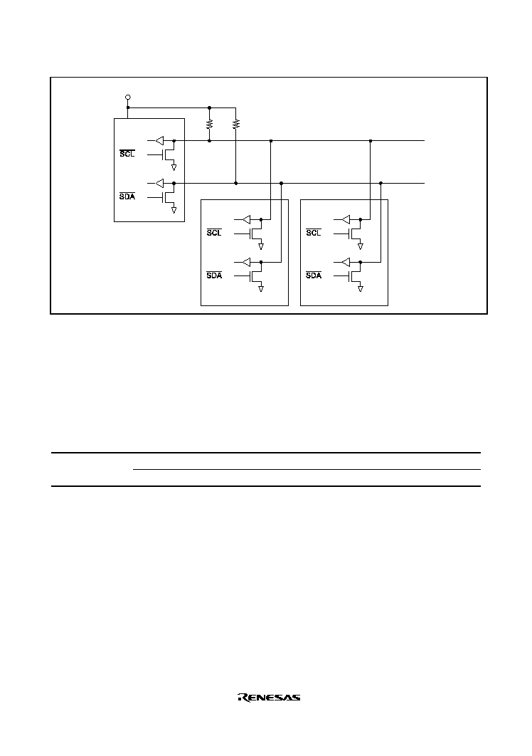
Rev. 2.0, 09/02, page 413 of 732
Vcc
Vcc
SCL
in
out
SCL
SDA
in
out
SDA
SCL
SDA
SCL
in
out
SCL
SDA
in
out
SDA
SCL
in
out
SCL
SDA
in
out
SDA
(Master)
This LSI
(Slave 1)
(Slave 2)
Figure 14.2 Example of the Connection of I
2
C Bus Interfaces
(This LSI is the Master Device)
14.2
Input/Output Pins
The I/O pins of the I
2
C bus interface are listed in table 14.1.
Table 14.1 Pin Configuration
Channel
Pin Name
*
I/O
Function
SCL0
I/O
Serial clock I/O pin
0
SDA0
I/O
Serial data I/O pin
Note:
*
In this manual, these pin names are abbreviated to SCL and SDA, respectively.

Rev. 2.0, 09/02, page 414 of 732
14.3
Description of Registers
The I
2
C bus interface includes the following registers. For the addresses of these registers and the
states of the registers in each state of processing, refer to section 25, List of Registers.
∑
I
2
C bus control register (ICCR)
∑
I
2
C bus status register (ICSR)
∑
I
2
C bus data register (ICDR)
∑
I
2
C bus mode register (ICMR)
∑
Slave-address register (SAR)
∑
Second slave-address register (SARX)
∑
Serial control register X (SCRX)
14.3.1
I
2
C Bus Data Register (ICDR)
ICDR is an 8-bit readable/writable register that holds the data for transmission during
transmission, and holds the received data during reception. Internally, ICDR consists of a shift
register (ICDRS), receive buffer (ICDRR), and transmission buffer (ICDRT).
ICDRS is the shift register and is not accessible from the CPU.
ICDRR is a read-only register; it stores data being received.
ICDRT is a write-only register; it stores data for transmission.
Data is automatically transferred between these three registers according to the bus state; this
affects the states of internal flags, such as TDRE and RDRF.
After one frame of data has been transmitted or received by ICDRS, and the next datum is present
in the ICDRT in the transmission mode (i.e., when the TDRE flag is 0), that datum is transferred
automatically from ICDRT to ICDRS. After ICDRS has received or transmitted one frame of data
in the receive mode, a datum in ICDRS is automatically transferred to ICDRR when the previous
datum is not present in ICDRR (i.e., when the RDRF flag is 0).
When, excluding the acknowledge bit, there are fewer than 8 bits in one frame, the alignment of
the data for transmission and of received data varies according to the setting of the MLS bit in
ICMR. Data for transmission should span the selected number of bits from the MSB when MLS =
0. When MLS is 1, the data should span the selected number of bits from the LSB. Received data
is read from the LSB when MLS is 0 and from the MSB when MLS is 1.
ICDR is assigned to the same address as SARX; it is only accessible when the ICE bit of ICCR is
set to 1.

Rev. 2.0, 09/02, page 415 of 732
The TDRE and RDRF flags are set/cleared under the following conditions. The setting of these
flags affects the state of the interrupt flag.
TDRE
Description
0
Transmission cannot be started or the next datum for transmission is present in the
ICDR (ICDRT).
(Initial Condition)
[Clearing conditions]
(1) In the transmission mode (TRS = 1), writing of a datum for transmission to ICDR
(ICDRT).
(2) In the I
2
C bus format or the serial format, detection of the stop condition from the
bus line's state after the issue of the stop-condition signal.
(3) Detection of the stop condition when the interface is in I
2
C bus format.
(4) In the receive mode (TRS = 0) (writing of 0 to TRS during transmission is enabled
after reception of a frame that includes the acknowledge bit).
1
The next datum for transmission can be written to ICDR (ICDRT).
[Setting conditions]
(1) Detection, by the I
2
C bus format or the serial format in the master mode
(TRS = 1), of the start condition from the bus line's state after the issue of the
start-condition signal.
(2) Transfer of data from ICDRT to ICDRS (data is transferred from ICDRT to ICDRS
when TRS = 1, TDRE = 0, and ICDRS is empty).
(3) Changing of the mode from reception (TRS = 0) to transmission (TRS = 1) after
detection of the start condition.
RDRF
Description
0
The datum in ICDR (ICDRR) is invalid.
(Initial Condition)
[Clearing condition]
When, in the receive mode, data received in ICDR (ICDRR) is read.
1
The data received in ICDR (ICDRR) can be read.
[Setting condition]
When data is transferred from ICDRS to ICDRR.
When the correct reception of data is allowed by TRS and RDRF both being 0, any
received data is transferred from ICDRS to ICDRR.

Rev. 2.0, 09/02, page 416 of 732
14.3.2
Slave-Address Register (SAR)
SAR is an 8-bit readable/writable register that is used to set the format and store the slave address.
When the interface is set for operation in the addressing format, the slave address in this register
has been enabled, and the upper 7 bits of the first frame to have been transmitted after satisfaction
of the start condition match the upper 7 bits of the value in SAR, this module has been designated,
by the master device, to act as a slave device. SAR is assigned to the same address as ICMR.
Reading from and writing to SAR is only enabled when the ICE bit in ICCR is set to 0.
Bit
Bit Name
Initial Value
R/W
Description
7
6
5
4
3
2
1
SVA6
SVA5
SVA4
SVA3
SVA2
SVA1
SVA0
0
0
0
0
0
0
0
R/W
R/W
R/W
R/W
R/W
R/W
R/W
Slave address
A unique address, which is different from the
slave address of any other device that is
connected to the I
2
C bus, is set in the SVA6 to
SVA0 bits.
0
FS
0
R/W
Format select
In conjunction with the FSX bit in SARX, this bit
selects the transfer format. For the slave mode,
the FS bit determines whether or not the slave
address in SAR is enabled. Table 14.2 shows
the settings selected by the values of these bits.

Rev. 2.0, 09/02, page 417 of 732
Table 14.2 Transfer Format
SAR
Bit 0
SARX
Bit 0
FS
FSX
Operating Mode
0
0
I
2
C bus format
∑
Enables the slave addresses in SAR and SARX
0
1
I
2
C bus format
∑
Enables the slave address in SAR
∑
Disables the slave address in SARX
1
0
I
2
C bus format
∑
Enables the slave address in SARX
∑
Disables the slave address in SAR
1
1
Clock- synchronous serial format
∑
Disables the slave addresses in SAR and SARX
14.3.3
Second Slave-Address Register (SARX)
SARX is an 8-bit readable/writable register that is used to set the format and store a second slave
address for the interface. When the interface is set for operation in the addressing format, the slave
address in this register has been enabled, and the upper 7 bits of the first frame to have been
transmitted after satisfaction of the start condition match the upper 7 bits of the value in SARX,
the interface has been designated, by the master device, to act as a slave device. SARX is assigned
to the same address as ICDR. Reading from and writing to SARX is only enabled when the ICE
bit in ICCR is set to 0.
Bit
Bit Name
Initial Value
R/W
Description
7
6
5
4
3
2
1
SVAX6
SVAX5
SVAX4
SVAX3
SVAX2
SVAX1
SVAX0
0
0
0
0
0
0
0
R/W
R/W
R/W
R/W
R/W
R/W
R/W
Second slave address
A unique address, which is different from the
slave address of any other device that is
connected to the I
2
C bus, is set in the SVAX6 to
SVAX0 bits.
0
FSX
1
R/W
Format select
In conjunction with the FS bit in SAR, this bit
selects the transfer format. For the slave mode,
the FSX bit determines whether or not the slave
address in SARX is enabled. Table 14.2, in the
above description of SAR, shows the settings
selected by the values of these bits.

Rev. 2.0, 09/02, page 418 of 732
14.3.4
I
2
C Bus Mode Register (ICMR)
ICMR is an 8-bit readable/writable register that selects transfer as MSB or LSB first, controls
waiting when the device is in the master mode, selects the frequency of the transfer clock for
master-mode operation, and the number of bits for transfer. ICMR is assigned to the same address
as SAR. ICMR is only accessible when the ICE bit in ICCR is set to 1.
Bit
Bit Name
Initial Value
R/W
Description
7
MLS
0
R/W
Selects MSB/LSB first
Selects whether data is transferred with the MSB
first or the LSB first.
When, excluding the acknowledge bit, there are
fewer than 8 bits in one frame, the alignment of the
data for transmission and of received data varies
according to the setting of the MLS bit in ICMR.
Data for transmission should span the selected
number of bits from the MSB when MLS = 0. When
MLS is 1, the data should span the selected number
of bits from the LSB. Received data is read from the
LSB when MLS =0 and from the MSB when MLS =
1.
When this module is being used in the I
2
C bus
format, do not set this bit to 1.
0: MSB first
1: LSB first

Rev. 2.0, 09/02, page 419 of 732
Bit
Bit Name
Initial Value
R/W
Description
6
WAIT
0
R/W
Wait-insertion bit
This bit determines whether or not, in the I
2
C bus
format in the master mode, the interface waits after
the data other than the acknowledge bit has been
transferred. When WAIT = 1 is set, the IRIC flag in
ICCR is set to 1 after the final bit of the data has
become low, and the interface enters the wait state
(SCL is low). Clearing the IRIC flag in ICCR to 0
cancels the wait state. The acknowledge bit is t(en
transferred. When WAIT is set to 0, no wait state is
inserted and the data and acknowledge bits are
continuously transferred. The IRIC flag in ICCR is
set to 1, regardless of the setting of the WAIT bit,
when the transfer of the acknowledge bit has been
completed.
In slave mode, this bit is disabled.
0: Data and acknowledge bits are continuously
transferred.
1: A wait state is inserted between transfer of the
data bits and of the acknowledge bit.
5
4
3
CKS2
CKS1
CKS0
0
0
0
R/W
R/W
R/W
Transfer clock select 2 to 0
The CKS2 to CKS0 bits, together with the IICX0 bit
in SCRX, select the frequency of the transfer clock.
This is used in the master mode. Set these bits to
obtain the required rate of transfer.
2
1
0
BC2
BC1
BC0
0
0
0
R/W
R/W
R/W
Bit counter
The BC2 to BC0 bits specify the number of bits to
be transferred in the next transfer. In transfer in the
I
2
C bus format (when the SAR FS bit or the SARX
FSX bit is 0), the data bits plus one acknowledge bit
are transferred. Set the BC2 to BC0 bits in the
intervals between the transfer of frames. Do not set
the BC2 to BC0 bits to 000 unless SCL is low.
The bit counter is initialized to 000 on a reset or on
detection of the start condition. In addition, this
counter returns to 000 on completion of the transfer
of all data bits and the acknowledge bit.

Rev. 2.0, 09/02, page 420 of 732
Table 14.3 Setting of the Transfer Clock
SCRX
Bit5
Bit5
Bit4
Bit3
Transfer Rate
IICX
CKS2
CKS1
CKS0
Clock
P
=
10MHz
P
=
16MHz
P
=
20MHz
P
=
25MHz
P
=
33MHz
P
=
40MHz
0
P
/28
357kHz
571kHz
714kHz
893kHz
1.18MH
z
1.43MH
z
0
1
P
/40
250kHz
400kHz
500kHz
625kHz
825kHz
1.00MH
z
0
P
/48
208kHz
333kHz
417kHz
521kHz
688kHz
833kHz
0
1
1
P
/64
156kHz
250kHz
313kHz
391kHz
516kHz
625kHz
0
P
/80
125kHz
200kHz
250kHz
313kHz
413kHz
500kHz
0
1
P
/100
100kHz
160kHz
200kHz
250kHz
330kHz
400kHz
0
P
/112
89.3kHz
143kHz
179kHz
223kHz
295kHz
357kHz
0
1
1
1
P
/128
78.1kHz
125kHz
156kHz
195kHz
258kHz
313kHz
0
P
/56
179kHz
286kHz
357kHz
446kHz
589kHz
714kHz
0
1
P
/80
125kHz
200kHz
250kHz
313kHz
413kHz
500kHz
0
P
/96
104kHz
167kHz
208kHz
260kHz
344kHz
417kHz
0
1
1
P
/128
78.1kHz
125kHz
156kHz
195kHz
258kHz
313kHz
0
P
/160
62.5kHz
100kHz
125kHz
156kHz
206kHz
250kHz
0
1
P
/200
50.0kHz
80.0kHz
100kHz
125kHz
165kHz
200kHz
0
P
/224
44.6kHz
71.4kHz
89.3kHz
112kHz
147kHz
177kHz
1
1
1
1
P
/256
39.1kHz
62.5kHz
78.1kHz
97.7kHz
129kHz
156kHz
Table 14.4 Setting of the Bit Counter
Bit2
Bit1
Bit0
Bits/frame
BC2
BC1
BC0
Clock- Synchronous
Serial Format
I
2
C Bus Format
0
8
9 (Initial value)
0
1
1
2
0
2
3
0
1
1
3
4
0
4
5
0
1
5
6
0
6
7
1
1
1
7
8

Rev. 2.0, 09/02, page 421 of 732
14.3.5
I
2
C Bus Control Register (ICCR)
ICCR is an 8-bit readable/writable register that selects operation or non-operation of the I
2
C bus
interface, enables/disables generation of the I
2
C-bus-interface interrupt signal, selects master/slave
mode, transmission/reception, enables/disables use of the acknowledge bit, confirms the state of
the bus attached to the I
2
C bus interface, sets the start/stop condition, and includes the interrupt
flag.
Bit
Bit
Name
Initial
Value
R/W
Description
7
ICE
0
R/W
I
2
C bus interface enable (ICE)
Determines whether or not the I
2
C bus interface is useable.
When this bit is set to 1, this module is set to the transfer-
enabled state. When this bit is cleared to 0, this module is
stopped, and its internal state is cleared.
0: This module is not operating.
The internal state of the I
2
C module is reinitialized.
Access to SAR and SARX is enabled.
1: This module is in its transfer-enabled state
Access to ICMR and ICDR is enabled.
6
IEIC
0
R/W
I
2
C-bus-interface interrupt enable
Determines whether to enable or disable issuing of this
interrupt from the I
2
C bus interface to the CPU.
0: Disables the interrupt
1: Enables the interrupt

Rev. 2.0, 09/02, page 422 of 732
Bit
Bit
Name
Initial
Value
R/W
Description
5
MST
0
R/W
Selects master or slave mode
This bit determines whether to use the I
2
C bus interface in
master mode or in slave mode.
0: Slave mode
[Clearing conditions]
(1) Writing of 0 to this bit by software
(2) When the master device in the I
2
C bus format starts
transmission and then fails because of a bus conflict.
1: Master mode
[Setting conditions]
(1) Writing of 1 to this bit by software (except when the 0 was
set by clearing condition (2))
(2) Writing of 1 to this bit after reading MST = 0 (when the 0
was set by clearing condition (2)).

Rev. 2.0, 09/02, page 423 of 732
Bit
Bit
Name
Initial
Value
R/W
Description
4
TRS
0
R/W
Selects transmission/reception
This bit determines whether the I
2
C bus interface is used in
receive mode or in transmit mode.
0: Receive mode
[Clearing conditions]
(1) Writing of 0 to this bit by software (except when the 1 was
set by setting condition (3))
(2) 0 is written after TRS = 1 is read (when the 1 was set by
setting condition (3))
(3) When the master device in the I
2
C bus format starts
transmission and then fails because of a bus conflict.
1: Transmit mode
[Setting conditions]
(1) Writing of 1 to this bit by software (except when the 1 was
set by clearing condition (3))
(2) Writing of 1 to this bit after reading TRS = 0 (when the 0
was set by clearing condition (3))
(3) When 1 is received as the R/W bit of the first frame in the
I
2
C bus format in slave mode.
When the addressing format (FS = 0 or FSX = 0) is used in the
slave-receive mode, transmission or reception is automatically
selected by the hardware, according to the setting of the R/W
bit of the first frame after the start condition has been satisfied.
Even if an attempt is made to change the TRS bit during the
transfer of data, the change is suspended until transmission of
the frame, including the acknowledge bit, has been completed;
the bit is then changed.

Rev. 2.0, 09/02, page 424 of 732
Bit
Bit
Name
Initial
Value
R/W
Description
3
ACKE
0
R/W
Enables/disables the acknowledge bit
This bit determines, for the I
2
C bus format, whether to ignore the
acknowledge bits returned from the receive device and thus
obtain continuous transfer or to perform error processing by
halting the transfer when the acknowledge bit is 1. When the
ACKE bit is 0, the value of the acknowledge bits that are
received do not affect the ACKB bit; the value in the ACKB bit
remains at 0.
The acknowledge bit is used in two different ways, depending
on the situation. One case is that the acknowledge bit is used
as a kind of flag to indicate whether or not processing for the
reception of data has been completed.
The other case is that acknowledge bit is fixed to 1.
0: The value of the acknowledge bit is ignored to allow the
continuous transfer of data.
1: Continuous data transfer is halted.
2
BBSY
0
R/W
Bus busy
The BBSY flag may be read to confirm whether or not the I
2
C
bus (SCL, SDA) has been released. In master mode, this bit is
used to set the start and stop conditions. When SDA changes
from high to low while SCL is high, the system regards the start
condition as having been set, and the BBSY flag is set to 1.
When SDA changes from low to high while SCL is high, the
system regards the stop condition as having been issued, and
the BBSY flag is cleared to 0.
When issuing the start condition, write 1 to BBSY and 0 to SCP.
When re-transmitting the start condition, follow the same
procedure. The stop condition is issued by writing 0 to BBSY
and SCP. Use the MOV instruction for these write operations.
Writing to the BBSY flag is disabled in slave mode. The I
2
C bus
interface must be set to master-transmission mode before the
start condition is issued. Before writing 1 to BBSY and 0 to
SCP, set MST and TRS to 1.
0: Bus-released state
[Clearing condition]
∑
Detection of the stop condition
1: Bus-occupied state
[Setting condition]
∑
Detection of the start condition

Rev. 2.0, 09/02, page 425 of 732
Bit
Bit
Name
Initial
Value
R/W
Description
1
IRIC
0
R/(W
)*
I
2
C-bus-interface interrupt-request flag
The IRIC flag indicates that the I
2
C bus interface has
generated an interrupt request for the CPU. When the slave
address or the general call address is detected in slave-
reception mode after the transfer of data has been
completed, when there is a failure because of bus conflict in
the master-transmission mode, and when the stop condition
is detected, the IRIC flag is set to 1. The timing with which
the IRIC flag is set changes according to the combination of
the values of the FS bit in SAR and the WAIT bit in ICMR.
Refer to section 14.4.6, Timing for Setting IRIC and the
Control of SCL. In addition, the condition on which the IRIC
flag is set changes according to the setting of the ACKE bit in
ICCR.
The IRIC flag is cleared by reading 1 from IRIC and then
writing 0.
When the DTC is used, the IRIC flag is automatically cleared;
this allows transfer to be continuous and without the
intervention of the CPU.
0: Transfer-wait state or during a transfer
1: An interrupt is generated.
For details, refer to table 14.5, Description of IRIC.
0
SCP
1
W
Start/stop condition issuance disabling bit
This bit controls issuing of the start/stop-condition signals in
master mode. When setting the start condition, write 1 to
BBSY and 0 to SCP. When re-transmitting the start condition,
follow the same procedure. The stop condition is set by
writing 0 to BBSY and SCP. When this bit is read, it always
returns 1. 1 written to this bit will not be stored.
0: In combination with the BBSY flag, issues the start/stop-
condition signals during writing.
1: When read, 1 is always returned. Writing to this bit is not a
valid operation.
Note:
*
It is only possible to write a 0 to this bit, to clear the flag.

Rev. 2.0, 09/02, page 426 of 732
Table 14.5 Description of IRIC
Bit1
IRIC
Description
0
While in transfer-wait state or during a transfer
[Clearing condition]
(1) Writing of 0 to this bit after reading IRIC = 1
(2) When reading from/writing to ICDR by DTC
(3) When the TDRE flag is cleared to 0
1
An interrupt is generated.
[Setting conditions]
∑
I
2
C bus format in master mode
(1) When the start condition is detected from the bus line's state after the start
condition has been set (i.e., when the TDRE flag has been set to 1 for
transmission of the first frame).
(2) When WAIT = 1, a wait is inserted between the data bits and the acknowledge bit.
(3) When the transfer of data has been completed (i.e., when the TDRE or RDRF flag
has been set to 1).
(4) When transfer has failed because of a bus conflict.
(5) When the ACKE bit is 1 and WAIT = 0, and 1 is received as an acknowledge bit
(i.e., when the ACKB bit is set to 1).
∑
I
2
C bus format in the slave mode
(1) When a slave address (SVA or SVAX) has been matched (i.e., when the AAS or
AASX flags have been set to 1), or when the re-transmission condition is satisfied
or the subsequent data transfer has been completed. (i.e., when the TDRE or
RDRF flag is set to 1)
(2) When the general call address has been detected (i.e., when the ADZ flag has
been set to 1) or when the re-transmission condition is satisfied or the subsequent
data transfer has been completed. (i.e., when the TDRE or RDRF flag is set to 1)
(3) When the ACKE bit is 1 and WAIT = 0, and 1 is received as an acknowledge bit
(i.e., when the ACKB bit is set to 1)
(4) When the stop condition is detected while the STOPIM bit in SCRX is set to 0
(i.e., when the SCRX STOPIM bit is set to 0, and the STOP or the ESTP flag is
set to 1)
∑
Clock synchronized serial format
(1) When the transfer of data has been completed (i.e., when the TDRE or the RDRF
flag has been set to 1)
(2) When the start condition has been detected while the interface is set for serial
format
Cases other than the above in which TDRE or RDRF is set to 1.

Rev. 2.0, 09/02, page 427 of 732
When the interface is in the I
2
C bus format and an interrupt is generated so that IRIC becomes 1,
other flags must be checked to locate the cause of the IRIC bit becoming 1. Each possible cause
has a corresponding flag. Precautions must be taken when the data transfer has been completed.
When the TDRE or RDRF flag, both of which are internal flags, is set, the IRTR flag, which is a
readable flag, may be set, but in some cases it will not be. In the I
2
C bus format in the slave mode,
the IRTR flag, which is the DTC-activation request flag, is not set during the period between the
completion of data transfer after a slave-address match or a general call address match and the
detection of the stop condition or transmission of the next start condition. Even when the IRIC or
IRTR flag has been set, the TDRE or RDRF flag, both of which are internal flags, may not be set
in some cases. When a continuous transfer is performed using the DTC, the IRIC or IRTR flag is
not cleared when the specified amount of data has been transferred. On the other hand, since the
specified number of read/write operations has been completed, the TDRE or the RDRF flag will
already have been cleared.
The relationship between the flags and the various states of transfer is shown in table 14.6.

Rev. 2.0, 09/02, page 428 of 732
Table 14.6 The Relationship between Flags and Transfer States
MST
TRS
BBSY
ESTP
STOP
IRTR
AASX
AL
AAS
ADZ
ACKB
State
1/0
1/0
0
0
0
0
0
0
0
0
0
Idle condition
(flag must be cleared.)
1
1
0
0
0
0
0
0
0
0
0
Start-condition issuance
1
1
1
0
0
1
0
0
0
0
0
Start-condition satisfaction
1
1/0
1
0
0
0
0
0
0
0
1/0
Master-mode wait
1
1/0
1
0
0
1
0
0
0
0
1/0
End of master-mode
transmission/reception
0
0
1
0
0
0
1/0
1
1/0
1/0
0
Arbitration lost
0
0
1
0
0
0
0
0
1
0
0
SAR match in the first
frame of slave-mode
operation
0
0
1
0
0
0
0
0
1
1
0
General call address match
0
0
1
0
0
0
1
0
0
0
0
SARX match
0
1/0
1
0
0
0
0
0
0
0
1/0
End of slave-mode
transmission/reception
(other than for an SARX
match)
0
0
1/0
1
1
1
0
0
0
0
1
0
1
1
0
0
0
0
0
0
0
1
End of slave-mode
transmission/reception
(other than for an SARX
match)
0
1/0
0
1/0
1/0
0
0
0
0
0
1/0
Stop-condition detection

Rev. 2.0, 09/02, page 429 of 732
14.3.6
I
2
C Bus Status Register (ICSR)
ICSR is an 8-bit readable/writable register that includes flags that indicate bus states and a bit for
the checking and control of the acknowledge signal.
Bit
Bit
Name
Initial
Value
R/W
Description
7
ESTP
0
R/(W)
*
Erroneous stop-condition detected
The ESTP flag indicates that the stop condition has been
detected during the transfer of a frame, in the I
2
C bus format
in the slave mode.
0: Erroneous-stop condition is not present
[Clearing condition]
(1) Writing of 0 to this bit after reading ESTP = 1
(2) Clearing of the IRIC flag to 0
1: An erroneous-stop condition has been detected in the I
2
C
bus format in the slave mode (this value has no meaning
when the interface is not in the I
2
C bus format in the slave
mode).
[Setting condition]
Detection of the stop condition during the transfer of a frame
6
STOP
0
R/(W)
*
Normal stop-condition detection flag
The STOP flag indicates that the stop condition has been
detected after the transfer of a frame in the I
2
C bus format in
the slave mode.
0: Normal stop-condition is not present.
[Clearing conditions]
(1) Writing of 0 to this bit after reading STOP = 1
(2) Clearing of the IRIC flag to 0
1: The normal stop condition has been detected in the I
2
C
bus format in the slave mode (this value has no meaning
when the interface is not in the I
2
C bus format in the slave
mode).
[Setting condition]
Detection of the stop condition after the transfer of a frame

Rev. 2.0, 09/02, page 430 of 732
Bit
Bit
Name
Initial
Value
R/W
Description
5
IRTR
0
R/(W)
*
I
2
C-bus-interface continuous transfer interrupt-request flag
The IRTR flag indicates that the I
2
C bus interface has
generated an interrupt for the CPU. The IRIC flag is set to
1 at the same time as the IRTR flag is set to 1.
The IRTR flag is set while the TDRE or RDRF flag is set to
1. The IRTR flag is cleared by reading an existing 1 from
and then writing a 0 to the flag. The IRTR flag is
automatically cleared when the IRIC flag is cleared.
0: Transfer-wait state or during transfer
[Clearing conditions]
(1) Writing of 0 to this bit after reading IRTR = 1
(2) Clearing of the IRIC flag to 0
1: Continuous-transfer state
[Setting conditions]
(1) Setting of the TDRE or RDRF flag to 1 while AASX is 1
in the I
2
C bus interface in the slave mode.
(2) Setting of the TDRE or RDRF flag to 1 when not in the
I
2
C bus interface in the slave mode.
4
AASX
0
R/(W)
*
Second slave-address detection flag
For the I
2
C bus interface in the slave mode, the AASX flag
is set to 1 when the first frame after the start condition
matches bits SVAX6 to SVAX0 of SARX.
To clear the AASX flag, read a 1 from and then write a 0 to
it. When the start condition is detected, the flag is
automatically cleared.
0: The second slave address of this device has not been
detected.
[Clearing conditions]
(1) Writing of 0 to this bit after reading AASX = 1
(2) Detection of the start condition.
(3) Entering master mode
1: This device's second slave address has been detected
[Setting condition]
(1) Detection of the second slave address in the slave
receive mode while FSX = 0.

Rev. 2.0, 09/02, page 431 of 732
Bit
Bit
Name
Initial
Value
R/W
Description
3
AL
0
R/(W)
*
Arbitration-lost flag
The AL flag indicates that the device, in master mode, has
failed to acquire bus-master status. The I
2
C bus interface
monitors the SDA as part of the method of bus arbitration.
When multiple masters make simultaneous attempts to use
the bus, the data on the line will eventually differ, for some of
the masters, from the data issued by the SDA. For such
masters, the AL flag is set to 1 as an indication that the bus is
occupied by another master.
To clear the AL flag, read a 1 from and then write a 0 to it. This
flag is automatically reset when ICDR is written to (during
transmission) or read (during reception).
0: Gaining the bus ownership
[Clearing conditions]
(1) Writing of data to ICDR (during transmission) or reading of
data from ICDR (during reception).
(2) Writing a 0 to this bit after reading it as 1
1: Lost the bus ownership
[Setting conditions]
(1) When the interface is in master-transmission mode, the
SDA value it is generating internally and the value on the
SDA pin do not match on the rising edge of SCL.
(2) When the start condition of another I
2
C device is detected
(i.e., when the interface is in master-transmission mode
and SCL goes high , and when the internal SDA and the
SDA pin do not match).

Rev. 2.0, 09/02, page 432 of 732
Bit
Bit
Name
Initial
Value
R/W
Description
2
AAS
0
R/(W)
*
Slave-address detection flag
When the first frame after the start condition matches the
SVA6 to SVA0 bits of SAR or when the general-call address
(H'00) is detected in the I
2
C bus interface in the slave-
reception mode, the AAS flag is set to 1.
To clear the AAS flag, read a 1 from and then write a 0 to it.
When ICDR is written to (during transmission) or read from
(during reception), the flag is automatically reset.
0: Neither this device's slave address nor the general call
address has been detected.
[Clearing conditions]
(1) Writing of data to ICDR (during transmission) or reading of
data from ICDR (during reception)
(2) Writing of 0 to this bit after reading it as 1
(3) Entering the master mode
1: The device's slave address or the general call address has
been detected.
[Setting condition]
Detection of the slave address or general call address while in
the slave-receive mode and FS = 0.
1
ADZ
0
R/(W)
*
General call address detection flag
In the I
2
C bus format in the slave-reception mode, the ADZ flag
is set to 1 when the general-call address (H'00) is detected in
the first frame after the start condition.
To clear the ADZ flag, read a 1 from and then write a 0 to it.
This flag is automatically reset when ICDR is written to (during
transmission) or read from (during reception).
0: The general call address has not been detected.
[Clearing conditions]
(1) Writing of data to ICDR (during transmission) or reading of
data from ICDR (during reception).
(2) Writing a 0 to this bit after reading it as 1
(3) Entering the master mode
1: The general call address has been detected.
[Setting condition]
Detection of the general call address in the slave-receive
mode (FSX = 0 or FS = 0).

Rev. 2.0, 09/02, page 433 of 732
Bit
Bit
Name
Initial Value
R/W
Description
0
ACKB
0
R/W
Acknowledge bit
The ACKB bit stores the acknowledgements.
When a given device is in the transmission mode, the
receiving device returns acknowledgements after the
receiving device has received data, and these
acknowledgements are loaded to the ACKB bit. After
the receiving device has received the data, it sends
the acknowledge bit that has been set in ACKB to the
transmitting device.
When this bit is read, the value that was loaded here
(the value returned from the receiving device) during
transmission (TRS = 1) is read. During receive
operations (TRS = 0), the value that was set is read
during receive.
0: While receiving, a 0 value is output according to
the timing for the output of the acknowledge bit.
This is the acknowledgement which is returned (0)
from the receiving device during transmission.
1: While receiving, a 1 value is also output according
to the timing for the output of the acknowledge bit.
This indicates that no acknowledgement has been
returned (1) from the receiving device during
transmission.
Note:
*
It is only possible to write a 0 to this bit, to clear the flag.

Rev. 2.0, 09/02, page 434 of 732
14.3.7
Serial Control Register X (SCRX)
SCRX is an 8-bit readable/writable register that controls register access and the I
2
C operating
mode. When the modules that are controlled by SCRX are not in use, do not write 1 to these bits.
Bit
Bit
Name
Initial Value
R/W
Description
7
6
0
0
R
R
These bits are reserved and always return 0 when
read, and should only be written with 0.
5
IICX0
0
R/W
I
2
C transfer-rate select 0
Along with bits CKS2 to CKS0 of ICMR, this bit selects
the transfer rate in the master mode. For details on
setting the transfer rate, refer to section 14.3.4, I
2
C Bus
Mode Register (ICMR).
4
IICE
0
R/W
I
2
C master enable
This bit controls access by the CPU to the data register
and control registers (ICCR, ICSR, ICDR/SARX, and
ICMR/SAR) of the I
2
C bus interface.
0: Disables CPU access to the data register and
control registers of the I
2
C bus interface.
1: Enables CPU access to the data register and control
registers of the I
2
C bus interface.
3
HNDS
0
*
R/W
Hand-shake receive bit
This bit enables/disables buffered operation in the
receive mode in the I
2
C bus format.
0: Enables buffered operation for reception
*
Receiving of the next frame proceeds even when
ICDR contains valid received data.
1: Disables buffered operation for reception
When ICDR contains valid received data, SCL is set
to its low level and receiving of the next frame of
data is thus suspended until the received data is
read from ICDR.

Rev. 2.0, 09/02, page 435 of 732
Bit
Bit
Name
Initial Value
R/W
Description
2
0
R
This bit is reserved and always returns 0 when read,
and should only be written with 0.
1
ICDRF0
0
R
This bit indicates whether or not ICDR contains valid
received data.
0: Indicates that ICDR does not contain valid received
data.
1: Indicates that ICDR contains valid received data.
0
STOPIM
0
R/W
Stop-condition-detected-interrupt mask
This bit enables/disables the issuing of stop-condition-
detected interrupt requests in the I
2
C bus format in the
slave mode.
0: This setting enables the stop-condition-detected
interrupt requests in the I
2
C bus format in the slave
mode.
1: This setting disables the stop-condition-detected
interrupt requests in the I
2
C bus format in the slave
mode.
Note:
*
Set this bit to 1.
14.4
Operation
14.4.1
I
2
C Bus Data Formats
The I
2
C bus interface is capable of transferring data in either the serial format or the I
2
C bus
format. The I
2
C bus format is referred to as an addressing format. The transfer of data in this
addressing format includes the transfer of acknowledge bits. This is shown in figures 14.3, (a) and
(b). The first frame after the start condition always consists of 8 bits.
The serial format is referred to as a `non-addressing format'. The transfer of data in this non-
addressing format does not include the transfer of an acknowledge bit. This is shown in figure
14.4. The I
2
C bus timing is shown in figure 14.5.
The symbols used in figures 14.3 to 14.5 are described in table 14.7.
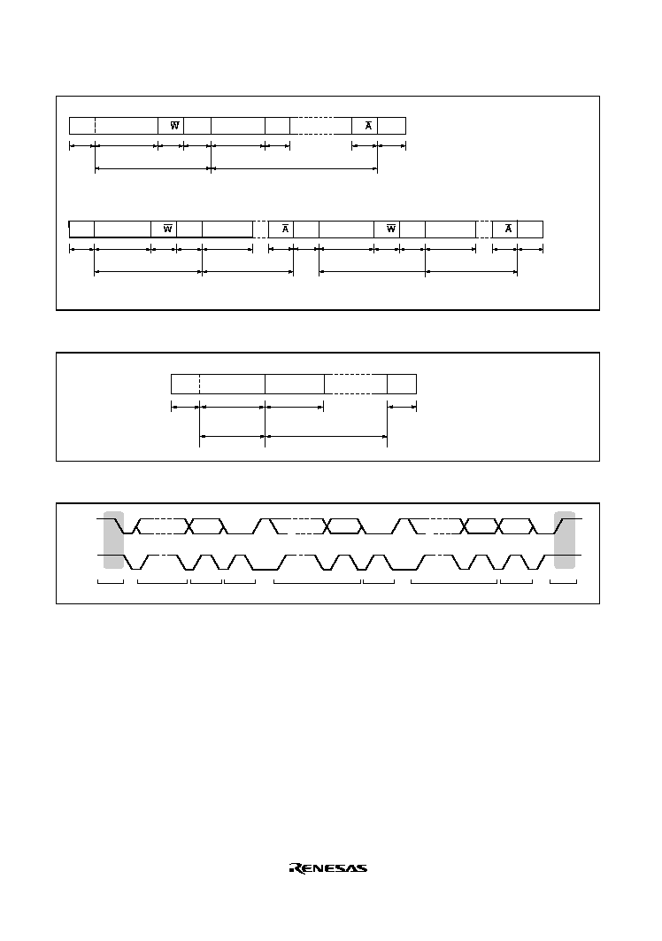
Rev. 2.0, 09/02, page 436 of 732
S
A
SLA
7
n
R/
DATA
A
1
1
m
1
1
1
A/
1
P
1
S
SLA
7
n1
7
R/
A
DATA
1
1
1
m1
1
A/
1
S
1
SLA
R/
1
1
m2
A
1
DATA
n2
A/
1
P
1
(a) FS=0 or FSX=0
Upper: Number of bits being transferred (n=1, n2=1 to 8)
Lower: Number of frames being transferred (m=1, m2=1 or above)
(b) When the start condition is re-transmitted, FS=0 or FSX=0
Number of bits
being transferred
(n=1 to 8)
Number of frames
being transferred
(m=1 or above)
Figure 14.3 I
2
C Bus Data Format 1 (I
2
C Bus Format)
S
DATA
8
n
DATA
FS=1 and FSX=1
Number of bits
being transferred
(n=1 to 8)
Number of frames
being transferred
(m=1 or above)
1
1
m
P
1
Figure 14.4 I
2
C Bus Data Format 2 (Serial Format)
SDA
SCL
S
SLA
R/W
A
9
8
1-7
9
8
1-7
9
8
1-7
DATA
A
DATA
A/A
P
Figure 14.5 I
2
C Bus Timing

Rev. 2.0, 09/02, page 437 of 732
Table 14.7 I
2
C Bus Data Format: Description of Symbols
S
This represents the start condition. The master device changes the level on SDA
from high to low while SCL is high.
SLA
This represents the slave address. The master device sends this to select the slave
device.
R/W
This represents the direction of transmission/reception. When the R/W bit is 1, data is
transferred from the slave to the master device. When the R/W bit is 0, data is
transferred from the master to the slave device.
A
This represents an acknowledgement. The receiving device sends this acknowledge
bit by setting the level on SDA to low (during master transmission, the slave returns
the acknowledge bits; during master reception, the master returns the acknowledge
bits).
DATA
This represents the transfer of data. The amount of bits to be transferred in each
such operation is set by the BC2 to BC0 bits of ICMR. The ICMR MLS bit determines
whether the data is transferred MSB first or LSB first.
P
This represents the stop condition. The master device changes the level on SDA from
low to high while SCL is high.
14.4.2
Operations in Master Transmission
In I
2
C bus format in the master transmission mode, the master device outputs the transmission
clock and data for transmission, and the slave device acknowledges its reception of data. The
following description gives the procedures for and operations of transmission.
1. Set the ICE bit in ICCR to 1. In addition, set the MLS and WAIT bits and the CKS2 to CKS0
bits of ICMR, and the IICX bit of SCRX, according to the operating mode.
2. Confirm that the bus is free by reading the BBSY flag in ICCR. Then set the MST and TRS
bits of ICCR to 1 to select the master-transmission mode. Then write 1 to BBSY and 0 to SCP.
This changes the level on SDA from high to low while SCL is high, and is thus the generation
of the start condition. The internal TDRE flag is thus set to 1, as are the IRIC and IRTR flags.
When the IEIC bit in ICCR has been set to 1, an interrupt request is generated for the CPU.
3. For a transfer in the I
2
C bus format (when the FS bit in SAR or the FSX bit in SARX is 0), the
first frame of data after the start condition includes the 7-bit slave address and the bit that
indicates the direction of the transfer operation as transmission or reception. The data for
transfer (slave address + R/W) is written to ICDR. In this case, the internal TDRE flag is
cleared to 0. The address data is transferred from ICDR to ICDRS, and the internal TDRE flag
is again set to 1. In this case, clear the IRIC flag to 0 so that the completion of this transfer can
be detected. The master device transmits the transmission clock signal and the data written in
the ICDR with the timing and in the order shown in figure 14.6. To acknowledge its selection,
the slave device that has been selected (that matches the slave address) sets the level on SDA
low in the 9th cycle of the transmission clock.
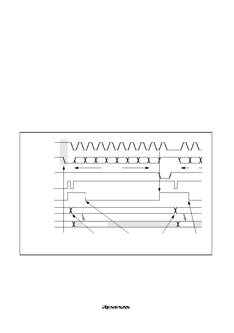
Rev. 2.0, 09/02, page 438 of 732
4. When the transmission of one frame has been completed, the IRIC flag is set to 1 on the rising
edge of the 9th cycle of the transmission clock. When the internal TDRE flag is set to 1 after
one frame has been transmitted, the level on SCL is automatically fixed low in synchronization
with the internal clock until the next datum for transmission has been written to ICDR.
5. When transmission is to be continued, the next datum for transmission is written to ICDR.
After that datum has been transferred to ICDRS and the internal TDRE flag has been set to 1,
clear the IRIC flag to 0. The next frame will be transmitted in synchronization with the internal
clock.
Data can be sequentially transmitted by repeatedly performing steps 4 and 5 above. When
terminating the transmission, clear the IRIC flag, write the H'FF to ICDR as a dummy after the
transmission of the final frame of data has been completed (when there is no further data for
transmission in ICDRT), then write 0 to the BBSY and SCP bits of ICCR to 0 at the point after the
IRIC flag has been set. When SCL is high, the level on SDA is changed from low to high to create
the stop condition.
2
1
2
1
4
3
6
5
8
7
9
IRIC
ICDRT
ICDRS
TDRE
SCL
(Master output)
SDA
(Master output)
SDA
(Slave output)
Address+R/W
Slave address
Data1
Data1
Data1
R/W
A
User processing
Slave address
Bit7
Bit6
Bit7
Bit6
Bit5
Bit4
Bit3
Bit2
Bit1
Bit0
Interrupt-request
generation
Interrupt-request
generation
Address+R/W
[4]
[2] Write 1 to BBSY and
0 to SCP (put the
start condition in place)
[3] ICDR write
[3] IRIC clear
[5] IRIC clear
[5] ICDR write
Note: The numbers in brackets [ ] represent step numbers in the above procedural description.
Start condition in place
Figure 14.6 An Example of the Timing of Operations in Master-Transmission Mode
(MLS = WAIT = 0)
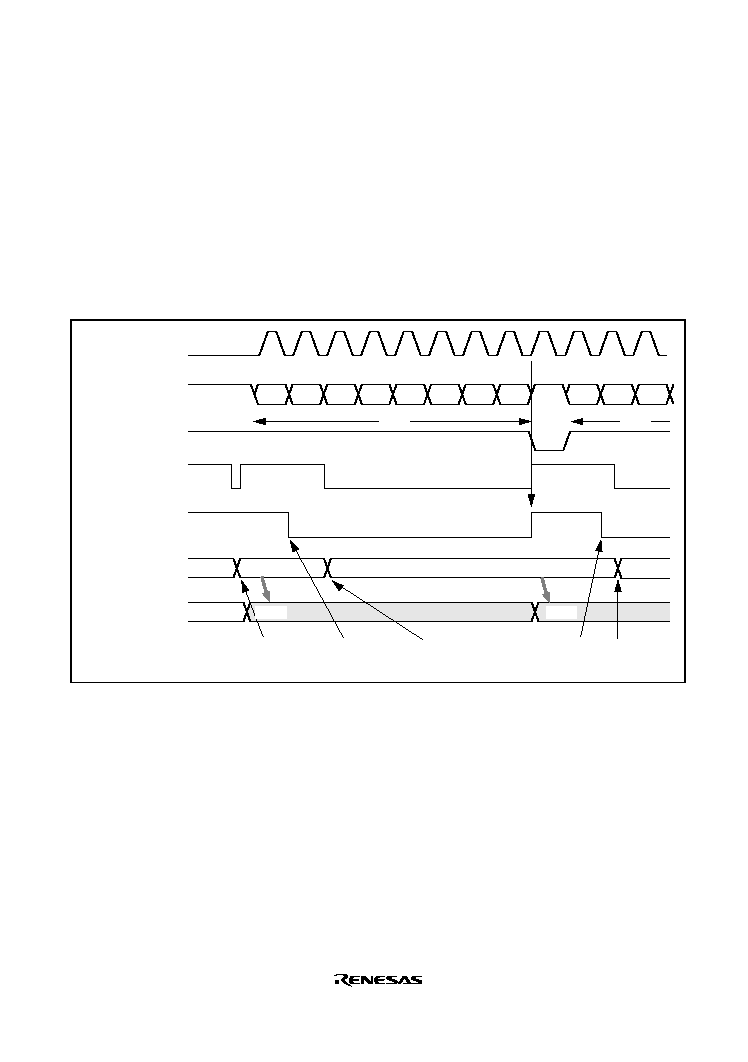
Rev. 2.0, 09/02, page 439 of 732
When continuously transmitting data,
6. Clear the IRIC flag to 0 before the rising edge of the 9th cycle of the transmission clock for the
data being transmitted, and write the next datum for transmission to ICDR.
7. When the transmission of one frame of data has been completed, the IRIC flag in ICCR is set
to 1 on the rising edge of the 9th cycle of the transmission clock. Concurrently, the next datum
for transmission is transferred from ICDR (ICDRT) to ICDRS, the internal TDRE flag is set to
1, and the next frame is transmitted in synchronization with the internal clock.
Steps 6 and 7 are repeated for the continuous transmission of data.
2
1
2
3
1
4
3
6
5
8
7
9
IRIC
ICDRT
ICDRS
TDRE
A
SCL
(Master output)
SDA
(Master output)
SDA
(Slave output)
Data2
Data1
Data2
Data1
Data3
Data2
Data1
User processing
Bit7
Bit6
Bit5
Bit7
Bit6
Bit5
Bit4
Bit3
Bit2
Bit1
Bit0
Interrupt-request
generation
ICDR write
[6] ICDR write
[6] ICDR write
[6] IRIC clear
[6] IRIC clear
Note: The numbers in brackets [ ] represent step numbers in the above procedural description.
[7]
[7]
Figure 14.7 An Example of the Continuous Transmission Timing in
Master-Transmission Mode (MLS = WAIT = 0)

Rev. 2.0, 09/02, page 440 of 732
14.4.3
Operations in Master Reception
In master-reception mode, the master device outputs the reception clock, receives data, and returns
acknowledgements of reception. The slave device transmits the data. The following description
gives the procedures for and operations of reception in master mode.
1. Clear the TRS bit in ICCR to 0 to change from the transmission mode to the reception mode.
In addition, clear the ACKB bit in ICSR to 0 (setting of the acknowledge bit).
2. When ICDR is read (a dummy read operation), the receiving of data starts; the receive clock is
output in synchronization with the internal clock, and the first datum is then received. To
determine the completion of its reception, clear the IRIC flag in ICCR.
3. The master device sets SDA to low on the 9th cycle of the receive clock and returns the
acknowledge bit. When the reception of one frame of data has been completed, the IRIC flag
in ICCR is set to 1 on the rising edge of the 9th cycle of the receive clock. When the IEIC bit
in ICCR has been set to 1, an interrupt request is generated for the CPU. In this case, if the
internal RDRF flag has been cleared to 0, the internal RDRF flag is set to 1 to continue with
reception. When the reception of the next frame is completed before the ICDR is read to clear
the IRIC flag as in step 4 below, SCL is automatically fixed to its low level in synchronization
with the internal clock.
4. Read ICDR to clear the IRIC flag in ICCR to 0. This clears the RDRF flag to 0.
Data can be continuously received by repeatedly performing steps 3 and 4 above. When receiving
is started by the change from master-transmission to master-reception mode, the internal RDRF
flag is cleared to 0. Initiation of the receiving of the next frame of data is thus automatic. To stop
receiving, the TRS bit must be set to 1 before the reception clock has started up for the next frame.
When stopping a receive operation, set the TRS bit to 1, read ICDR, and then write 0 to the BBSY
and the SCP bits of ICCR. By doing so, the level on SDA is changed from low to high while SCL
is high, and this is the stop condition.
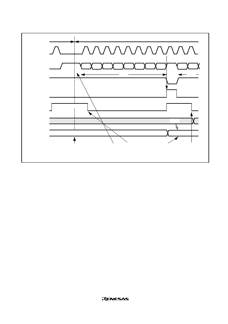
Rev. 2.0, 09/02, page 441 of 732
2
1
2
1
4
3
6
5
8
7
9
9
IRIC
ICDRS
ICDRR
RDRF
A
A
SCL
(Master output)
SDA
(Slave output)
SDA
(Master output)
Data1
Data2
Data1
Data1
User processing
Bit7
Bit6
Bit7
Bit6
Bit5
Bit4
Bit3
Bit2
Bit1
Bit0
Interrupt-request
generation
Interrupt-request
generation
[2] ICDR read
(dummy read)
[2] IRIC clear
[4] ICDR read
[4] IRIC clear
[1] TRS is cleared to 0
Note: The numbers in brackets [ ] represent step numbers in the above procedural description.
[3]
Master-transmission mode
Master-reception mode
Figure 14.8 An Example of the Timing of Operations in Master-Reception Mode
(MLS = WAIT = ACKB = 0)

Rev. 2.0, 09/02, page 442 of 732
14.4.4
Operations in Slave Reception
In the slave-reception mode, the master device transmits the transmission clock and data, and the
slave device returns acknowledgements of reception. The following description gives the
procedures for and operations of receiving in slave mode.
1. Set the ICE bit of ICCR to 1. In addition, set the MLS bit of ICMR and the MST and TRS bits
of ICCR to the values required for the mode of operation.
2. When the output of a start condition by the master device is detected, the BBSY flag in ICCR
is set to 1.
3. When the slave address of the target device matches the address sent in the first frame after the
start condition, it has been designated to act as a slave device by the master device. When the
8th bit of data (R/W) is 0, the TRS bit in ICCR remains 0; the device receives in slave mode.
4. To acknowledge its selection, the slave device sets the level on SDA low on the 9th cycle of
the receive frame. The IRIC flag in ICCR is concurrently set to 1, which, when the IEIC bit in
ICCR is set to 1, generates an interrupt request for the CPU. When the internal RDRF flag has
been cleared to 0, the internal RDRF flag is set to 1, and receiving continues. While the
internal RDRF flag is set to 1, the slave device keeps the level on SCL to low from the falling
edge of the receive clock until the current datum has been read to ICDR.
5. ICDR is read and the IRIC flag in ICCR is cleared to 0. In this case, the RDRF flag is cleared
to 0.
Data is continuously received by repeatedly performing steps 4 and 5 above. When the stop
condition is detected, i.e., when the level on SDA goes from low to high while SCL is high, the
BBSY flag in ICCR is cleared to 0.
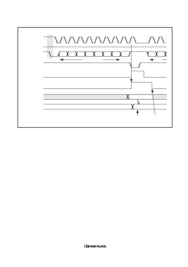
Rev. 2.0, 09/02, page 443 of 732
2
1
2
1
4
3
6
5
8
7
9
IRIC
ICDRS
ICDRR
RDRF
A
R/W
SCL
(Master output)
SDA
(Master output)
SCL
(Slave output)
SDA
(Slave output)
Address+R/W
Slave address
Data1
User processing
Bit7
Bit6
Bit7
Bit6
Bit5
Bit4
Bit3
Bit2
Bit1
Bit0
Interrupt-request
generation
Address+R/W
[5] ICDR read
[5] IRIC clear
Note: The numbers in brackets [ ] represent step numbers in the above procedural description.
[4]
Start condition in place
Figure 14.9 An Example of the Timing of Operations in Slave-Reception Mode (1)
(MLS = ACKB = 0)
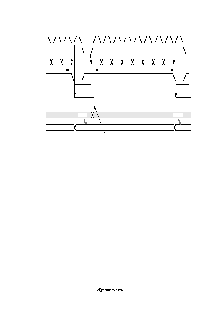
Rev. 2.0, 09/02, page 444 of 732
2
1
4
3
6
5
8
7
9
8
7
9
IRIC
ICDRS
ICDRR
RDRF
A
A
SCL
(Master output)
SDA
(Master output)
SCL
(Slave output)
SDA
(Slave output)
Data2
Data2
Data1
Data1
Data1
Data2
Bit7
Bit6
Bit5
Bit4
Bit3
Bit2
Bit1
Bit0
Bit1
Bit0
Interrupt-request
generation
Interrupt-request
generation
Note: The numbers in brackets [ ] represent step numbers in the above procedural description.
User processing
[5] ICDR read [5] IRIC clear
[4]
[4]
Figure 14.10 An Example of the Timing of Operations in Slave-Reception Mode (2)
(MLS = ACKB = 0)

Rev. 2.0, 09/02, page 445 of 732
14.4.5
Operations in Slave Transmission
In the slave-transmission mode, the slave device transmits data while the master device outputs the
reception clock and returns acknowledgements of reception. The following description gives the
procedures for and operations of transmitting in slave mode.
1. Set the ICE bit of ICCR to 1. In addition, set the MLS bit of ICMR and the MST and TRS bits
of ICCR to the values required for the mode of operation.
2. When the slave address of the target device matches the address sent in the first frame after the
start condition has been detected, the slave device sets the level on SDA low over the 9th cycle
of the clock to acknowledge its selection. The IRIC flag in ICCR is concurrently set to 1,
which, when the IEIC bit in ICCR is set to 1, generates an interrupt request for the CPU. When
the 8th bit of data (R/W) is 1, the TRS bit in ICCS is set to 1, and this automatically places the
device in the slave-transmission mode. In this case, the TDRE flag is set to 1. The slave device
sets the level on SCL low from the falling edge of the transmission clock until the first datum
for transmission is written to ICDR.
3. After 0 has been written to the IRIC flag, data is written to ICDR. In this case, the internal
TDRE flag is cleared to 0. The written data is transferred to ICDRS, and the internal TDRE
flag, the ICIR and IRTR flags are again set to 1. After clearing the IRIC flag to 0, the next
datum for transmission is written to ICDR. The slave device sequentially transmits the bits of
data written in ICDR, on the basis of the clock from the master device, and with the timing
shown in figure 14.11.
4. After the transmission of one frame has been completed, the IRIC flag in ICCR is set to 1 on
the rising edge of the 9th cycle of the transmission clock. When the internal TDRE flag is set
to 1, the slave device sets the level on SCL low from the falling edge of the transmission clock
until the next datum for transmission is written to ICDR. The master device sets SDA low on
the 9th cycle and then returns the acknowledgement that it has received the current datum. The
acknowledge signal is stored in the ACKB bit in ICSR and this makes it possible to confirm
that the transfer was completed normally. When the internal TDRE flag is 0, the bits in the
ICDR are transferred to ICDRS and transmission starts. The internal TDRE flag, and the IRIC
and the IRTR flags are then set to 1 again.
5. To continue with the transmission, clear the IRIC flag to 0 and write the next datum for
transmission to ICDR. In this case, the internal TDRE flag is cleared to 0.
Data is continuously transmitted by repeatedly performing steps 4 and 5 above. When completing
the transmission, write H'FF to ICDR. When the stop condition is detected, i.e., when the level on
SDA goes from low to high while SCL is high, the BBSY flag in ICCR is cleared to 0.
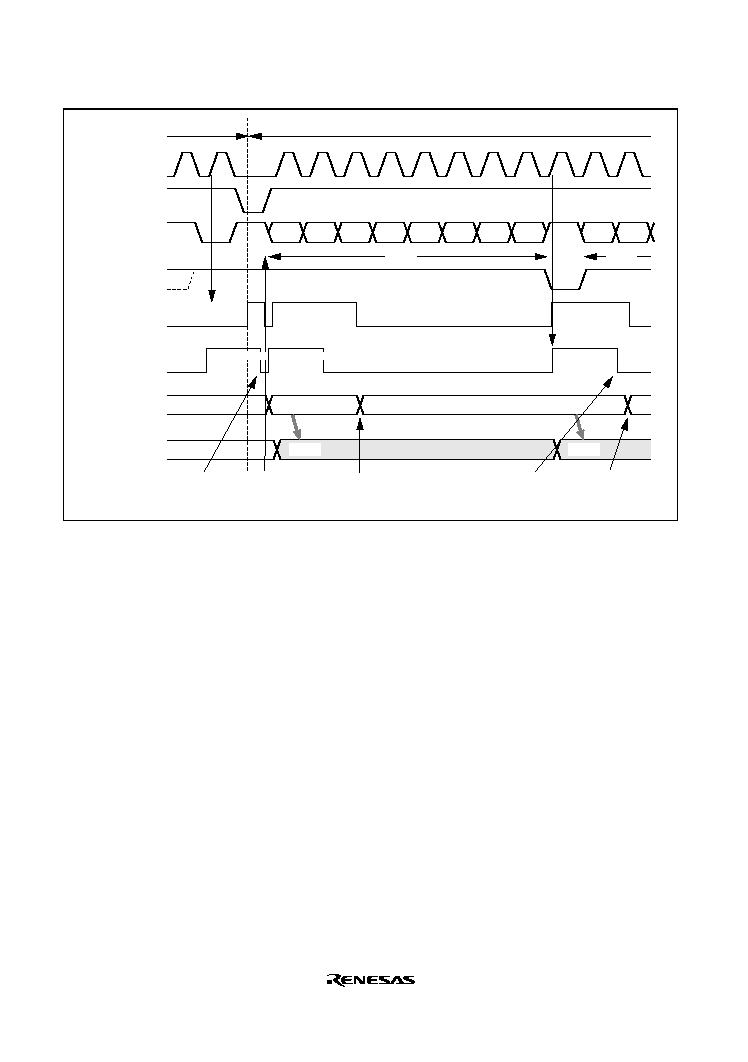
Rev. 2.0, 09/02, page 446 of 732
2
1
2
1
4
3
6
5
8
7
9
9
8
IRIC
ICDRS
ICDRT
TDRE
A
R/W
A
SCL
(Master output)
SDA
(Master output)
SCL
(Slave output)
SDA
(Slave output)
Data2
Data1
Data2
Data1
Data1
Data2
User processing
Bit7
Bit6
Bit7
Bit6
Bit5
Bit4
Bit3
Bit2
Bit1
Bit0
Interrupt-request
generation
Interrupt-request
generation
Interrupt-request
generation
[5] ICDR write
[5] IRIC clear
[3] ICDR write
[3] ICDR write
[3] IRIC clear
Note: The numbers in brackets [ ] represent step numbers in the above procedural description.
[3]
[2]
Slave-transmission mode
Master-reception mode
Figure 14.11 An Example of the Timing of Operations in Slave-Transmission Mode
(MLS = 0)
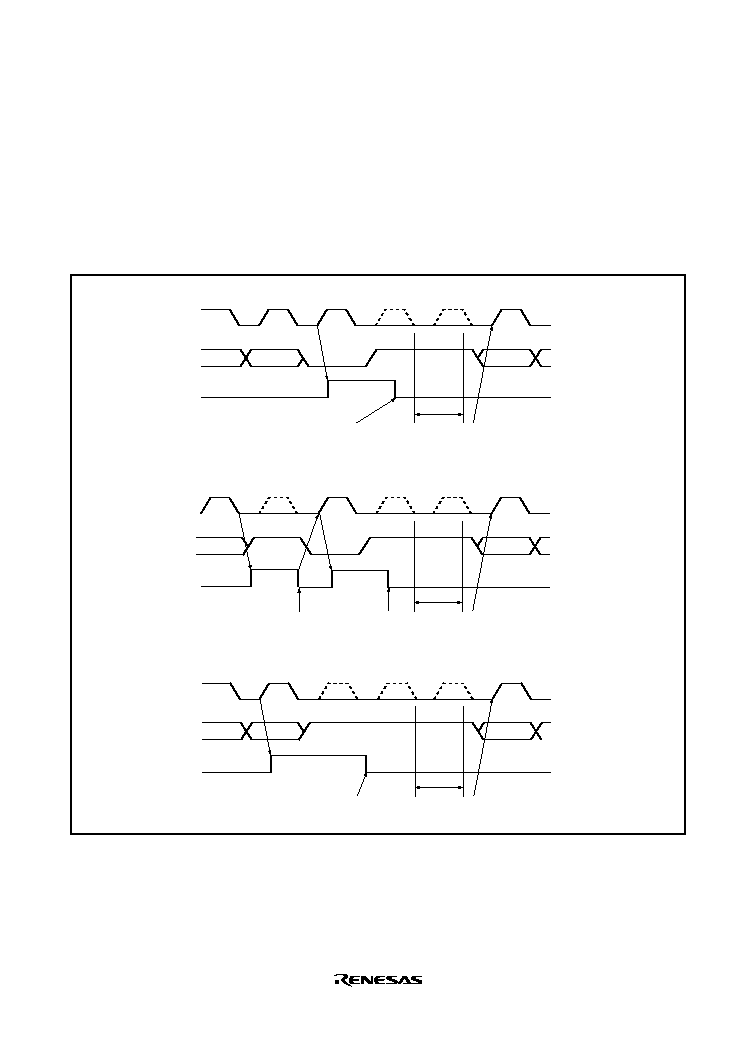
Rev. 2.0, 09/02, page 447 of 732
14.4.6
Timing for Setting IRIC and the Control of SCL
The timing with which the interrupt-request flag (IRIC) is set varies according to the settings of
the WAIT bit in ICMR, FS bit in SAR, and the FSX bit in SARX. When the TDRE and RDRF
internal flags are set to 1, the level on SCL is automatically set low in synchronization with the
internal clock after the transfer of one frame of data. Figure 14.12 shows the timing with which
IRIC is set and the control of SCL.
SCL
SDA
IRIC
1
A
8
7
1
9
8
7
SCL
SDA
IRIC
1
A
8
1
9
8
SCL
SDA
IRIC
1
8
7
1
8
7
(a) When WAIT=0, and FS=0 or FSX=0 (I
2
C bus format, no wait )
(b) When WAIT=1, and FS=0 or FSX=0 (I
2
C bus format, wait inserted )
(c) When FS=1 and FSX=1 (clock-synchronized serial format )
User processing
IRIC clear
ICDR write (during transmission) or
ICDR read (during reception)
User processing
IRIC clear
ICDR write (during transmission) or
ICDR read (during reception)
User processing
IRIC clear
IRIC clear
ICDR write (during transmission) or
ICDR read (during reception)
Figure 14.12 IRIC-Set Timing and the Control of SCL
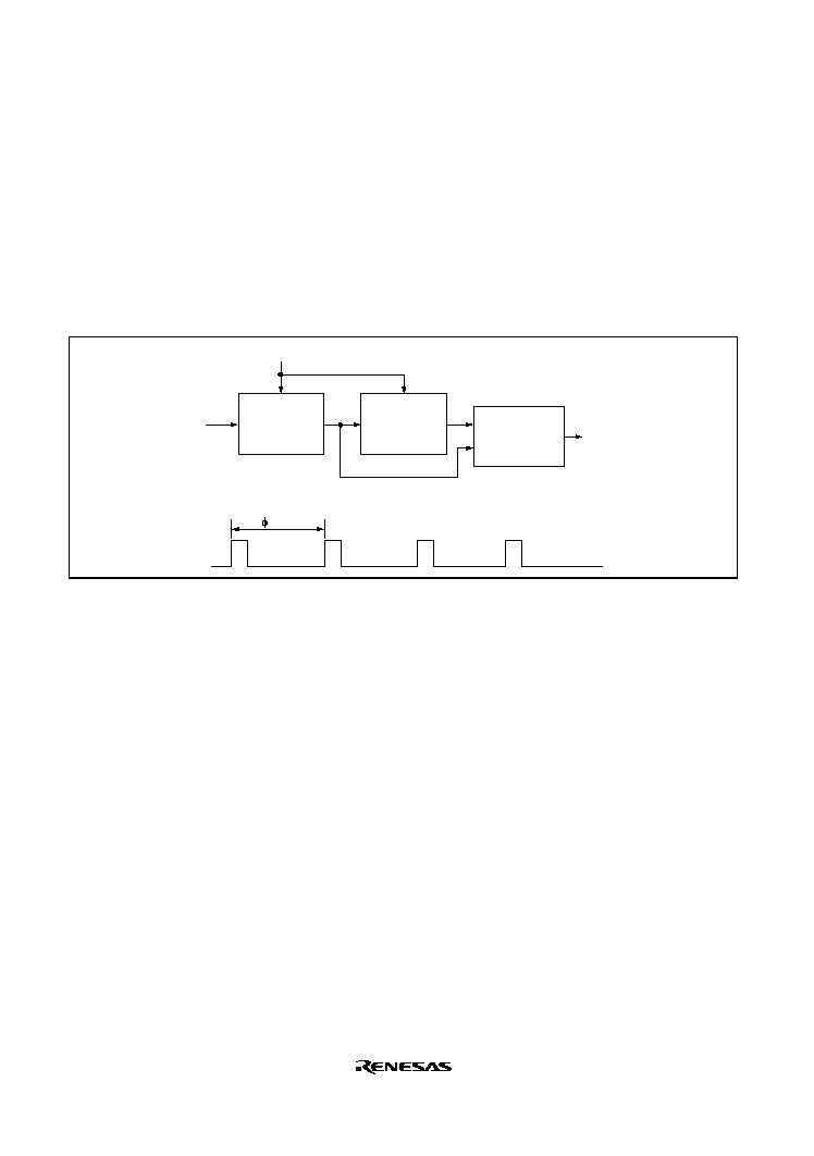
Rev. 2.0, 09/02, page 448 of 732
14.4.7
Noise Canceller
The states on the SCL and SDA pins are fetched internally via the noise canceller. Figure 14.13 is
a block diagram of the noise canceller.
The noise canceller consists of a 2-stage latch circuit and match-detection circuit, which are
connected in series. The input signal on the SCL pin (or on the SDA pin) is sampled at the interval
P
; when the two latch outputs match, the given level is then sent to the next stage. If the two
values don't match, the existing value is maintained.
C
Q
D
C
Q
D
Sampling clock
Sampling clock
SCL input signal or
SDA input signal
Latch
Latch
Match-detection
circuit
P period
Internal SCL signal or
Internal SDA signal
Figure 14.13 A Block Diagram of the Noise Canceller

Rev. 2.0, 09/02, page 449 of 732
14.4.8
DTC Operation
In the I
2
C bus format, since the slave device or the direction of transfer is selected by the slave
address or the R/W bit, and the acknowledge bit may indicate the end of reception or reception of
the final frame, the continuous transfer of data by the DTC must be combined with interrupt-
driven processing by the CPU.
Table 14.8 shows examples of processes in which the DTC is used. For the slave-mode processes,
it is assumed that the amount of data to be transferred is defined in advance.
Table 14.8 Examples of Operations in which the DTC is Used
Item
Master-
transmission
mode
Master-
reception mode
Slave-
transmission
mode
Slave-reception
mode
Transfer of slave
address + R/W
bit
DTC
transmission
(ICDR write)
CPU
transmission
(ICDR write)
CPU reception
(ICDR read)
CPU reception
(ICDR read)
Dummy-data
read
CPU processing
(ICDR read)
Main unit data
transfer
DTC
transmission
(ICDR write)
DTC reception
(ICDR read)
DTC
transmission
(ICDR write)
DTC reception
(ICDR read)
Dummy-data
(H
FF) write
DTC processing
(ICDR write)
Final frame
processing
Unnecessary
CPU reception
(ICDR read)
Unnecessary
CPU reception
(ICDR read)
Transfer-request
processing after
processing of the
final frame
First time:
Clearing by the
CPU
Second time:
Generation of
the end
condition by the
CPU
Unnecessary
Dummy data:
H
FF is
transmitted and
detected as the
end condition
and is
automatically
cleared
Unnecessary
Setting, in DTC,
the number of
frames of data to
be transferred
Transmission:
Number of
actual frames of
data + 1 (+1
represents the
frame for slave
address + R/W
bits)
Reception:
Number of
actual frames of
data
Transmission:
Number of
actual frames of
data + 1 (+1
represents
dummy data
(H
FF))
Reception:
Number of
actual frames of
data
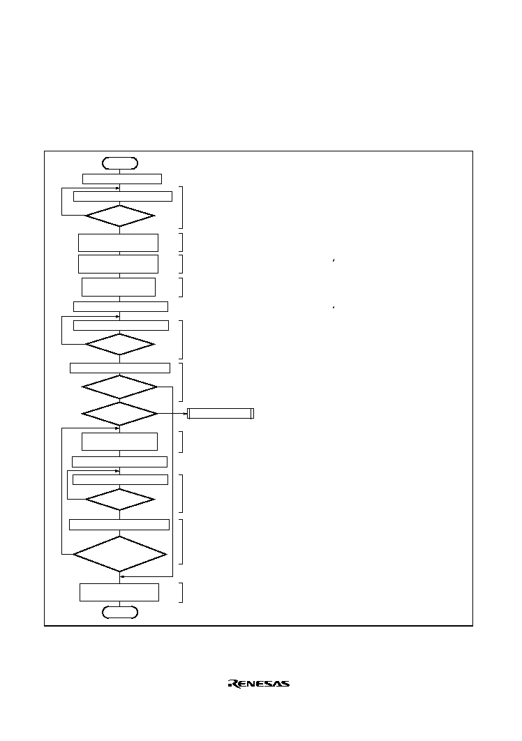
Rev. 2.0, 09/02, page 450 of 732
14.4.9
Using the Interface: Some Examples
Figures 14.14 to 14.17 are flow charts that give examples of the use of the I
2
C bus interface in
each of its modes.
BBSY=0?
No
IRIC=1?
No
No
Yes
Yes
Yes
IRIC=1?
No
No
No
Yes
Yes
Yes
Start
Initial setting
Read the BBSY flag (ICCR)
Set MST=1 and
TRS=1 (ICCR)
Write BBSY=1 and
SCP=0 (ICCR)
Write BBSY=0,
SCP=0 (ICCR)
Write the data for
transmission to ICDR
Write the data for
transmission to ICDR
Clear the IRIC flag (ICCR)
Clear the IRIC flag (ICCR)
Read the ACKB bit (ICSR)
Read the ACKB bit (ICSR)
Read the IRIC flag (ICCR)
Read the IRIC flag (ICCR)
Transmission
mode?
ACKB=0?
End
Transmission
completed?
(ACKB=1?)
Master reception
[1]
[2]
[3]
[4]
[5]
[6]
[7]
[8]
[9]
[10]
[1] Determine the states of the SCL and SDA lines.
[2] Set the device to the master-transmission mode.
[3] Generate the start condition.
[4] Set the first byte of data for transmission (slave address+R/W).
[5] Wait for the end of the current byte s transmission.
[6] Test for reception of the acknowledge bit from the specified slave device.
[7] Set the second and subsequent bytes of data for transmission.
[8] Wait for the end of the current byte s transmission.
[9] Test for the end of transmission.
[10] Generate the stop condition.
Figure 14.14 Example: Flowchart of Operations in the Master-Transmission Mode
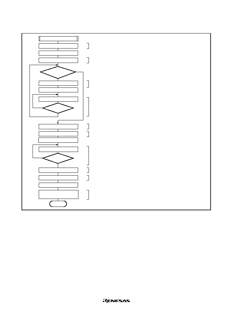
Rev. 2.0, 09/02, page 451 of 732
No
No
Yes
Yes
No
Yes
IRIC=1?
IRIC=1?
Set TRS=0 (ICCR)
Set TRS=1 (ICCR)
Set ACKB=0 (ICSR)
Set ACKB=1 (ICSR)
Write 0 to BBSY
and SCP (ICCR)
Final receive
operation?
Clear the IRIC flag (ICCR)
Clear the IRIC flag (ICCR)
Clear the IRIC flag (ICCR)
Clear the IRIC flag (ICCR)
Read the IRIC flag (ICCR)
Read the IRIC flag (ICCR)
Read ICDR
Read ICDR
Read ICDR
End
Master-reception mode
[1]
[2]
[3]
[4]
[5]
[6]
[7]
[8]
[9]
[10]
[1] Set the reception mode.
[2] Set the acknowledge bit.
[3] Start of reception (dummy read as the first operation).
[4] Wait for the reception of one byte.
[5] Set the acknowledgement for the final receive operation.
[6] Start the final receive operation.
[7] Wait for the reception of one byte.
[8] Set the device to the transmission mode.
[9] Read the data received in the final frame (When ICDR is read and the
device is not set to the transmission mode, a receive operation starts).
[10] Generate the stop condition.
Figure 14.15 Example: Flowchart of Operations in the Master-Reception Mode
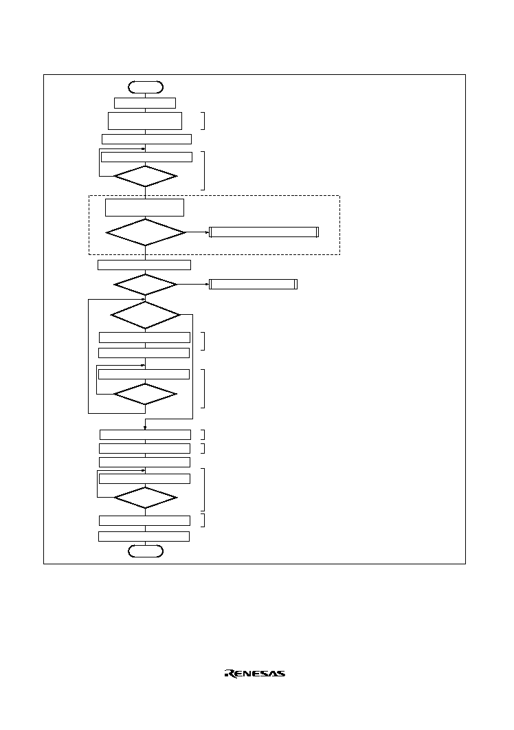
Rev. 2.0, 09/02, page 452 of 732
No
Yes
No
Yes
No
No
Yes
Yes
Yes
No
No
Yes
AAS=1 and
ADZ=0?
IRIC=1?
TRS=0?
IRIC=1?
IRIC=1?
Start
Initial setting
Set MST=0,
TRS=0 (ICCR)
Clear the IRIC flag (ICCR)
Clear the IRIC flag (ICCR)
Clear the IRIC flag (ICCR)
Read the AAS and
ADZ flags (ICSR)
Read the IRIC flag (ICCR)
Read the IRIC flag (ICCR)
Read the IRIC flag (ICCR)
End
[1]
[2]
[3]
[4]
[5]
[6]
[7]
[8]
Read ICDR
Read ICDR
Read ICDR
Set ACKB=0 (ICSR)
Set ACKB=0 (ICSR)
Final receive
operation?
General call address processing
Read the TRS bit (ICCR)
Slave-transmission mode
[1] Set the device to the slave-reception mode.
[2] Wait for one byte to be recieved (slave address).
[3] Start of reception (dummy read as the first operation).
[4] Wait for the completion of reception.
[5] Set the acknowledgement for the final receive operation.
[6] Start the final receive operation.
[7] Wait for the end of the receive operation.
[8] Read the last data to be received.
*
Explanation omission
Figure 14.16 Example: Flowchart of Operations in the Slave-Reception Mode
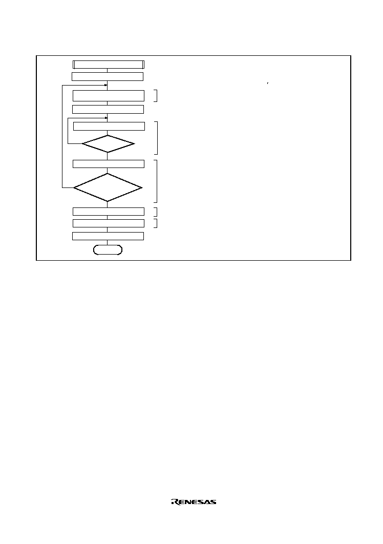
Rev. 2.0, 09/02, page 453 of 732
Yes
Yes
No
No
IRIC=1?
Clear the IRIC flag (ICCR)
Clear the IRIC flag (ICCR)
Clear the IRIC flag (ICCR)
Read the IRIC flag (ICCR)
End
[1]
[2]
[3]
[4]
[5]
Slave-transmission mode
Write the data for
transmission to ICDR
Read the ACKB bit (ICSR)
Transmission
complated?
(ACKB=1?)
Set TRS=0 (ICCR)
Read ICDR
[1] Set the data for the second and subsequent transmissions.
[2] Wait for the end of the current byte s transmission.
[3] Test for the end of transmission.
[4] Set the device to the slave-reception mode.
[5] Dummy read (to release the SCL line).
Figure 14.17 Example: Flowchart of Operations in the Slave-Transmission Mode
14.5
Usage Notes
1. In master mode, when the instruction that generates the start condition is issued immediately
after the instruction that generates the stop condition, neither the start condition nor the stop
condition will be correctly output. For the consecutive output of the start condition and stop
condition, read the port after issuing the instruction that generates the start condition, and make
sure that the levels on both SCL and SDA are low. Then issue the instruction that generates the
stop condition. Note that SCL may not have completely reached its low level when BBSY
becomes 0.
2. The following two conditions apply to the start of the next transfer: take note when reading
from/writing to ICDR.
a. ICE = 1, TRS = 1, and data is written to ICDR (including automatic transfer from ICDRT
to ICDRS)
b. ICE = 1, TRS = 0, and data is read from ICDR (including automatic transfer from ICDRS
to ICDRR)
3. In synchronization with the internal clock, SCL and SDA are output with the timing shown in
table 14.9. The timing on the bus is determined by the rise/fall times of the signals, and these
are affected by the bus-load's capacitance, series resistance, and parallel resistance.

Rev. 2.0, 09/02, page 454 of 732
Table 14.9 I
2
C Bus Timing (output of SCL and SDA)
Item
Symbol
Output Timing
Unit
Remarks
SCL-output cycle time
t
SCLO
28 t
pcyc
to 256 t
pcyc
ns
SCL-output high-pulse width
t
SCLHO
0.5 t
SCLO
ns
SCL-output low-pulse width
t
SCLLO
0.5 t
SCLO
ns
SDA-output bus-free time
t
BUFO
0.5 t
SCLO
-
1 t
pcyc
ns
Start-condition-output hold time
t
STAHO
0.5 t
SCLO
-
1 t
pcyc
ns
Output setup time for re-transmission of
start condition
t
STASO
1 t
SCLO
ns
Setup time for output of the stop condition
t
STOSO
0.5 t
SCLO
+2 t
pcyc
ns
Setup time for the output of data (master)
1 t
SCLLO
-
3 t
pcyc
ns
Setup time for the output of data (slave)
t
SDASO
1 t
SCLL
-
3 t
pcyc
ns
Data-output hold time
t
SDAHO
3 t
pcyc
ns
4. The SCL and SDA inputs are sampled in synchronization with P
. Therefore, the AC timing
depends on the period of P
cycle t
pcyc
. When the P
frequency does not reach 5 MHz, the AC
timing specifications of the I
2
C bus interface are not satisfied.
5. The SCL rising time t
Sr
is defined as being within 1,000 ns (300 ns in the high-speed mode).
The I
2
C bus interface monitors SCL in the master mode, and communication is synchronized
in a bit-by-bit basis. When the rise time t
Sr
(the time required to reach V
IH
from an initially low
level) of SCL exceeds the time determined by the input clock of the I
2
C bus interface, the high-
level period of SCL is extended. The time SCL takes to rise is determined by the pull-up
resistance and the load capacitance. Therefore, to operate at the specified transfer rate, set the
pull-up resistance and load capacitance so that each time is within the corresponding value
given in table 14.10.

Rev. 2.0, 09/02, page 455 of 732
Table 14.10 Tolerance of the SCL Rise Time (t
Sr
)
Time [ns]
IICX
t
pcyc
I
2
C bus
specification
(max)
P
=
10MHz
P
=
16MHz
P
=
20MHz
P
=
25MHz
P
=
33MHz
P
=
40MHz
Standard
mode
1000
750
468
375
300
227
188
0
7.5
t
pcyc
High-
speed
mode
300
227
188
Standard
mode
1000
875
700
530
438
1
17.5
t
pcyc
High-
speed
mode
300
6. The rise and fall times of SCL and SDA are respectively prescribed as being 1000 ns or less
and 300 ns or less by the I
2
C bus specification. The output timing of SCL and SDA for the I
2
C
bus interface of this LSI are described by t
SCLD
and t
pcyc
as shown in table 14.9. However, due to
the effect of the rise and fall times, the I
2
C bus interface specifications are not satisfied at the
maximum transfer rate. Table 14.11 shows the results of calculating the output timing for each
available operating frequency, by considering the worst-case rise and fall times. t
BUFO
does not
satisfy the specifications of the I
2
C bus interface specifications. As a countermeasure against
this problem, either (a) ensure that your program provides the required interval (approximately
1
µ
s) between issuing of the stop condition and of the next start condition or (b) select a slave
device with an input timing that permits use with this output timing for connection to the I
2
C
bus.
For t
SCLLO
in the high-speed mode and t
STASO
in the standard mode, the I
2
C bus interface specification
is not satisfied when the worst case for t
Sr
/t
Sf
is assumed. Take one of the following steps:
a. Adjust the rise and fall times by changing the pull-up resistors and load capacitance.
b. Reduce the transfer rate until the specification is satisfied.
c.
For connection to the I
2
C bus, select a slave device with an input timing that permits use
with this output timing.

Rev. 2.0, 09/02, page 456 of 732
Table 14.11 I
2
C Bus Timing (when the effect of t
Sr
/t
Sf
is at its maximum)
Time (at Maximum Transfer Rate) [ns]
Item
t
pcyc
Effect
of t
Sr
/t
Sf
(max)
I
2
C bus
specification
(min)
P
=
10MHz
P
=
16MHz
P
=
20MHz
P
=
25MHz
P
=
33MHz
P
=
40MHz
Standard
mode
-
1000
4000
4000
4000
4000
4000
4000
4000
t
SCLHO
0.5 t
SCLO
(
-
t
Sr
)
High-speed
mode
-
300
600
950
950
950
950
950
950
Standard
mode
-
250
4700
4750
4750
4750
4750
4750
4750
t
SCLLO
0.5 t
SCLO
(
-
t
Sf
)
High-speed
mode
-
250
1300
1000
*
1
1000
*
1
1000
*
1
1000
*
1
1000
*
1
1000
*
1
Standard
mode
-
1000
4700
3900
*
1
3938
*
1
3950
*
1
3960
*
1
3970
*
1
3975
*
1
t
BUFO
0.5 t
SCLO
-
1 t
pcyc
(
-
t
Sr
)
High-speed
mode
-
300
1300
850
*
1
888
*
1
900
*
1
910
*
1
920
*
1
925
*
1

Rev. 2.0, 09/02, page 457 of 732
Time (at Maximum Transfer Rate) [ns]
Item
t
pcyc
Effect
of t
Sr
/t
Sf
(max)
I
2
C bus
specification
(min)
P
=
10MHz
P
=
16MHz
P
=
20MHz
P
=
25MHz
P
=
33MHz
P
=
40MHz
Standard
mode
-
250
4000
4650
4688
4700
4710
4720
4725
t
STAHO
0.5 t
SCLO
-
1 t
pcyc
(
-
t
Sf
)
High-speed
mode
-
250
600
900
938
950
960
970
975
Standard
mode
-
1000
4700
9000
9000
9000
9000
9000
9000
t
STASO
1 t
SCLO
(
-
t
Sr
)
High-speed
mode
-
300
600
2200
2200
2200
2200
2200
2200
Standard
mode
-
1000
4000
4200
4125
4100
4080
4061
4050
t
STOSO
0.5 t
SCLO
+2 t
pcyc
(
-
t
Sr
)
High-speed
mode
-
300
600
1150
1075
1050
1030
1011
1000
Standard
mode
-
1000
250
3400
3513
3550
3580
3609
3625
t
SDASO
As
mast
er
1 t
SCLLO
*
2
-
3 t
pcyc
(
-
t
Sr
)
High-speed
mode
-
300
100
700
813
850
880
909
925
Standard
mode
-
1000
250
3400
3513
3550
3580
3609
3625
t
SDASO
As
slave
1 t
SCLL
*
2
-
3 t
pcyc
*
2
(
-
t
Sr
)
High-speed
mode
-
300
100
700
813
850
880
909
925
Standard
mode
0
0
300
188
150
120
91
75
t
SDAHO
3 t
pcyc
High-speed
mode
0
0
300
188
150
120
91
75
Notes: 1. Apply one or more of the following measures to satisfy the I
2
C bus interface
specification.
∑
Ensure that the interval between the setting of the start condition and of the stop
condition is sufficient.
∑
Adjust the rise and fall times by changing the values of the pull-up resistors and load
capacitance.
∑
Adjust the system by decreasing the transfer rate.
∑
Select a slave device with an input timing that permits the I/O timing.
The values in the above table are changed by the setting of the IICX bit and the CKS2
to CKS0 bits. Since the maximum transfer rate may not be achievable, depending on
the frequency, check whether or not the I
2
C bus interface specification is satisfied under
the actual conditions that are set.
2. Calculated from the I
2
C bus specifications (standard 4700 ns/min, high-speed: 1300
ns/min.)
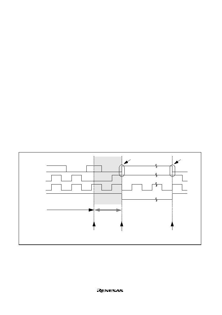
Rev. 2.0, 09/02, page 458 of 732
7. Points for caution when reading ICDR at the end of master reception
To halt the reception of data after a receive operation in the master-reception mode has been
completed, set the TRS bit to 1 and write 0 to BBSY and SCP. By doing so, the level on SDA
will be changed from low to high while SCL is high, that is, the stop condition will be
generated. The received data can be read by reading ICDR. If there is data in the buffer,
however, the data received in ICDRS cannot be transferred to ICDR. Therefore, the second-
byte of data cannot be read.
When reading of the second-byte of data is required, set the stop condition in the master-
reception mode (with the TRS bit being 0). When reading the received data, confirm that the
BBSY bit in ICCR is 0, the stop condition has been generated, and the bus is released. After
that, read the ICDR register while TRS is 0.
In this case, if an attempt is made to read the received data (data in ICDR) during the period
from the execution of the instruction (write 0 to BBSY and SCP of ICCR) that sets the stop
condition and the actual generation of the stop condition, it is not possible to generate the clock
correctly for a the subsequent master transmission.
Rewriting of the I
2
C control bit to change the mode of operation or setting of
transmission/reception, such as clearing of the MST bit after the completion of
transmission/reception by the master, must not take place in any period other than period (a)
(after confirming that the BBSY bit in ICCR has been cleared to 0) in figure 14.18.
SDA
SCL
A
8
9
Bit 0
Internal clock
BBSY bit
Stop condition
Start condition
Master-reception mode
ICDR read-disabled
period
Execution of the instruction
that sets the stop condition
(writing 0 to BBSY and SCP)
Confirmation of stop-condition
(reading 0 from BBSY)
Start condition set
(a)
Figure 14.18 Points for Caution in Reading Data Received by Master Reception
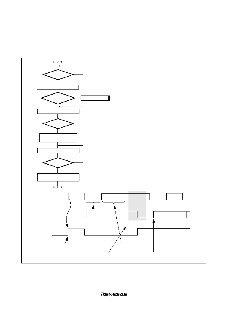
Rev. 2.0, 09/02, page 459 of 732
8. Points for Caution in Setting the Start Condition for Re-transmission
Figure 14.19 shows the timing and flowchart of the setting of the start condition for re-
transmission, and the timing with which the data is continuously written to ICDR.
Yes
Yes
Yes
Yes
No
No
No
No
SDA
ACK
bit7
IRIC
SCL
IRIC=1?
SCL=Low?
SCL=High?
Clear IRIC in ICSR
Set the start
condition?
Read the SCL pin
Other processing
Write 1 to BBSY and
0 to SCP of ICSR
Read the SCL pin
Write the data for
transmission to ICDR
[1]
[2]
[3]
[4]
[5]
[1] Wait for completion of one-byte transfer.
[2] Decide whether or not SCL is low.
[3] Execuse the instruction that sets the start
condition for re-transmission.
[4] Decide whether or not SCL is high.
[5] Set the data for transmission (slave address+R/W)
[1] Tasting of IRIC
[2] Testing of SCL=Low
[3] Instruction that puts the
start condition in place
[4] Testing of SCL=high
Start condition
(re-transmission)
[5] Write to ICDR
Note: Program so that steps 3 to 5 above are
executed continuously.
Figure 14.19 Flowchart and Timing of the Execution of the Instruction that Sets the Start
Condition for Re-Transmission
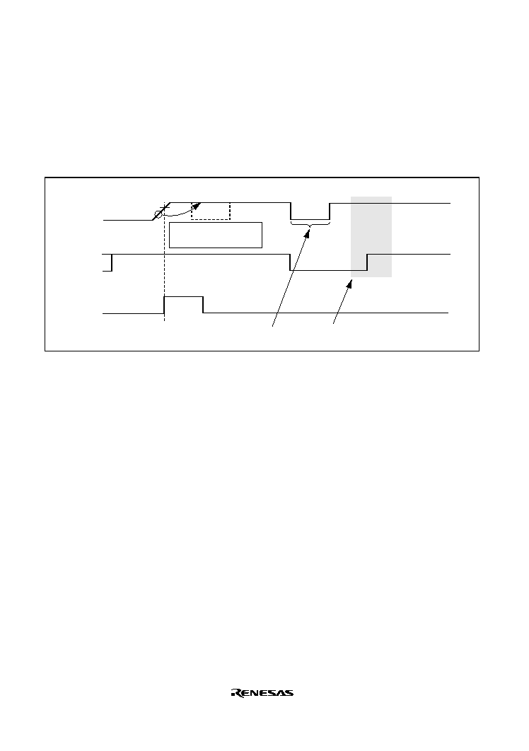
Rev. 2.0, 09/02, page 460 of 732
9. Points for Caution in the Execution of the Instruction that Sets the I
2
C Bus Interface Stop
Condition
If the rise time in the 9
th
cycle of SCL exceeds the specified value due to a high bus-load
capacitance, or if a slave device inserts a wait by setting the level on SCL low, read SCL in the
following way to confirm that the level is low, and then execute the instruction that sets the
stop condition.
SDA
IRIC
SCL
VIH
9
th
cycle
Period for securing
the high-level period
SCL is detected as low
since this waveform takes
a long time to rise.
Stop condition
[1] Decision on whether
or not SCL is low
[2] Execution of the instruction
that sets the Stop Condition
Figure 14.20 Timing for the Setting of the Stop Condition
10. Set the HNDS bit in serial control register X (SCRX) to 1.
11. In slave transmit operation of the I
2
C bus interface module, when ICDR is read from or ICCR
is read from or written to at the moment address reception is switched to data transmission,
erroneous data may be transmitted.
In normal transmit operation, when a first frame is received and the received address matches,
the TRS bit is automatically set to 1 and transmit mode is entered if the R/W bit of the 8th
clock cycle is 1. The SCL pin is then fixed to low from the fall of the 9th clock of the first
frame until the transmit data is written to the ICDR register.
However, when ICDR is read from or ICCR is read from or written to within 6 peripheral
clock cycles (half-tone dot-meshing area in figure 14.21) after the rising edge of the 9th
transmit/receive clock for address reception of the first frame, the SCL pin is not fixed low
after the fall of the 9th clock for the first frame. The master device starts sending clock signals
before the slave device has written transmit data to ICDR. As a result, data in the ICDR shift
register is output to the SDA pin, and erroneous data is transmitted to the master device.
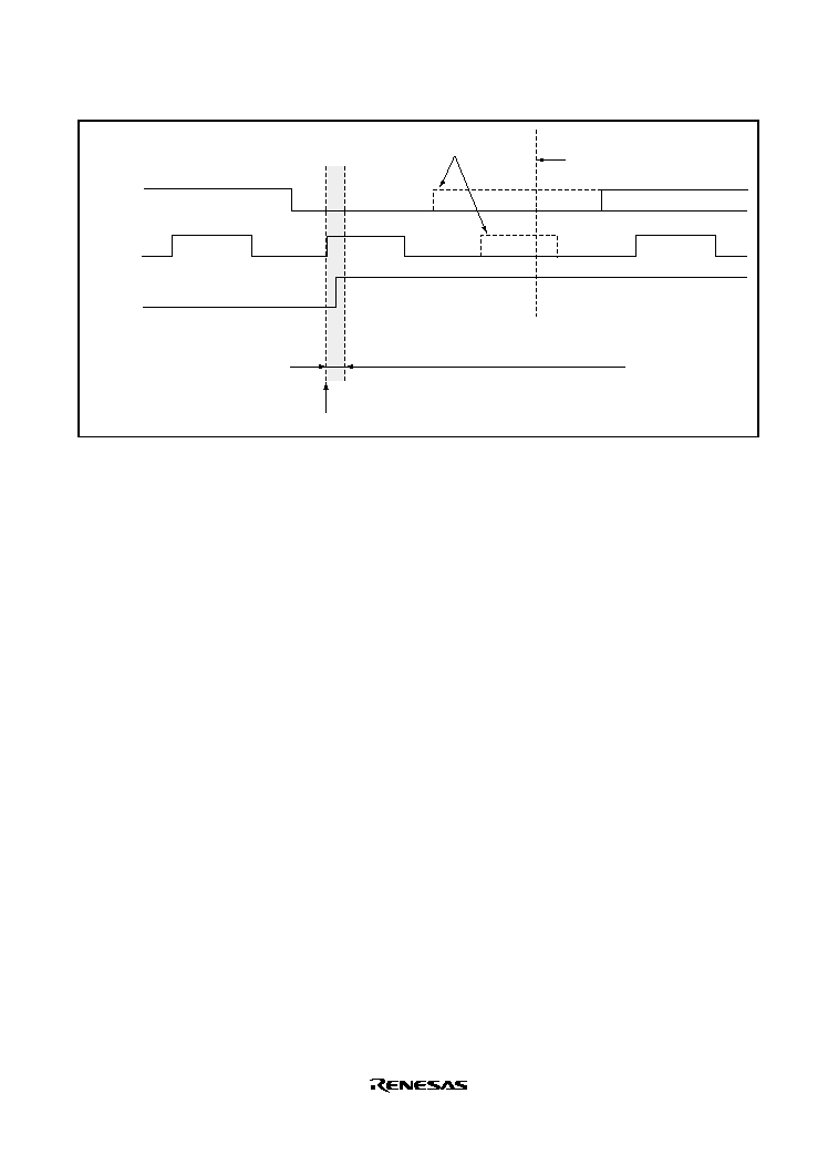
Rev. 2.0, 09/02, page 461 of 732
SDA
SCL
TRS bit
R/W
A
Bit 7
Data transmission
8
9
Address reception
Write to ICDR
Period in which read from ICDR and read from
or write to ICDR are prohibited
(6 peripheral clocks)
Detection of rise of 9th transmit/receive clock
Erroneous waveforms
Figure 14.21 Scheme of Slave Transmit Operation
In slave transmit operation, do not read from ICDR or read from or write to ICCR during the
period indicated by half-tone dot-meshing in figure 14.21.
For the interrupt processing that normally occurs in synchronization with the rising edge of the
9th transmit/receive clock, reading from ICDR or reading from or writing to ICCR causes no
problems because the prohibited period ends before transiting to the interrupt processing.
To ensure that this interrupt processing is carried out, satisfy either of the following conditions.
(1) Before the next slave address reception starts, complete the ICDR read operation and ICCR
read/write operation.
(2) Monitor the BC2 to BC0 bits (bit counters 2 to 0) in ICMR, and when the BC2 to BC0 bits
are all cleared to 0 (8th or 9th clock), wait for at least two transmit/receive clocks before
reading from ICDR or reading from or writing to ICCR to avoid the period in which these
operations will cause a failure.
12. To change, without transiting to the stop condition, from slave transmit operation (TRS = 1) to
next address receive operation (TRS = 0) by the input of resumption condition, clear TRS to 0
during time period (a) in figure 14.22, when the I
2
C bus interface is in slave mode.
In slave mode, the TRS bit setting in ICCR becomes valid as soon as the bit is set during the
period from when the rising edge of the 9th clock or a stop condition is detected to the next
rising edge at the SCL pin (period (a) in figure 14.22).
However, for any other period (i.e., period (b) in figure 14.22), the TRS bit setting is retained
until the next rising edge of the 9th clock or a stop condition is detected, so that the TRS bit
setting does not become valid immediately.
Accordingly, in the address reception following input of a resumption condition, the internally
effective TRS bit setting remains 1 (transmit mode), and the acknowledge bit that should be
transmitted at the end of address reception is not transmitted at the 9th transmit/receive clock.
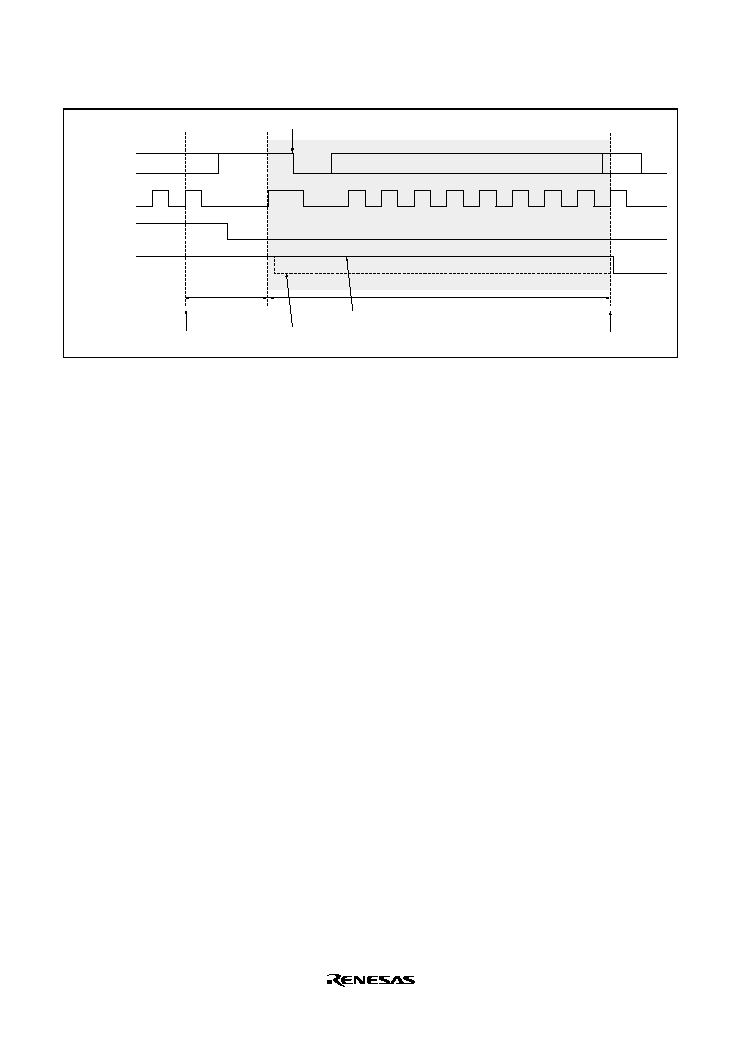
Rev. 2.0, 09/02, page 462 of 732
Resumption condition
1
2
3
4
5
6
7
8
9
8
9
(a)
(b)
SDA
SCL
(a) TRS bit
(b) TRS bit
A
Detection of rise of 9th
transmit/receive clock
Detection of rise of 9th
transmit/receive clock
TRS bit setting value
TRS bit effective value
Period in which TRS bit setting is retained
Address reception
Data
transmission
Figure 14.22 Scheme of TRS Bit Setting in Slave Mode

ADCMS20B_010020020700
Rev. 2.0, 09/02, page 463 of 732
Section 15 A/D Converter
This LSI includes a successive approximation type 10-bit A/D converter. The block diagram of the
A/D converter is shown in figure 15.1.
15.1
Features
∑
10-bit resolution
∑
Input channels
8 channels (two independent A/D conversion modules)
∑
Conversion time: 5.4 µs per channel (at P
= 25 MHz operation), 6.7µs per channel (at P
= 20
MHz operation)
∑
Three operating modes
Single mode: Single-channel A/D conversion
Continuous scan mode: Continuous A/D conversion on 1 to 4 channels
Single-cycle scan mode: Single-cycle A/D conversion on 1 to 4 channels
∑
Data registers
Conversion results are held in a 16-bit data register for each channel
∑
Sample and hold function
∑
Three methods for conversion start
Software
Conversion start trigger from multifunction timer pulse unit (MTU)
External trigger signal
∑
Interrupt request
An A/D conversion end interrupt request (ADI) can be generated
∑
Module standby mode can be set
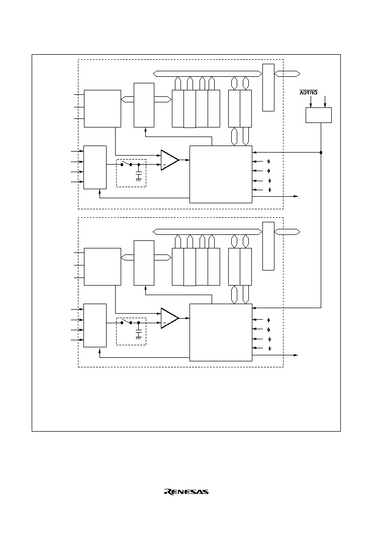
Rev. 2.0, 09/02, page 464 of 732
Control circuit
Control circuit
+
P /8
MTU
trigger
AN0
AN1
AN2
AN3
P /4
P /16
AV
CC
AV
ref
AV
SS
ADDR0
ADCSR_0
ADCR_0
ADDR1
ADDR2
ADTSR
ADDR3
ADI0(DTC)
interrupt signal
P /32
P /8
P /4
P /16
P /32
(only for SH7145)
(only for SH7145)
10-bit
D/A
A/D0
A/D1
+
AN4
AN5
AN6
AN7
AV
CC
AV
ref
AV
SS
ADDR4
ADCSR_1
ADCR_1
ADDR5
ADDR6
ADDR7
ADI1
(DMAC/DTC)
interrupt signal
ADCR_0
ADCSR_0
ADDR0
ADDR1
ADDR2
ADDR3
: A/D0 control register
: A/D0 control/status register
: A/D0 data register 0
: A/D0 data register 1
: A/D0 data register 2
: A/D0 data register 3
: A/D1 control register
: A/D1 control/status register
: A/D1 data register 4
: A/D1 data register 5
: A/D1 data register 6
: A/D1 data register 7
ADCR_1
ADCSR_1
ADDR4
ADDR5
ADDR6
ADDR7
Bus interface
Bus interface
Legend:
Sample-and-hold circuit
Comparator
Comparator
Analog
m
ultiple
x
e
r
Analog
m
ultiple
x
e
r
Sample-and-hold circuit
Successive
approximations
register
10-bit
D/A
Successive
approximations
register
Module data bus
Module data bus
Figure 15.1 Block Diagram of A/D Converter (For One Module)

Rev. 2.0, 09/02, page 465 of 732
15.2
Input/Output Pins
Table 15.1 summarizes the input pins used by the A/D converter. This LSI has two A/D
conversion modules, each of which can be operated independently. The input channels are divided
into four channel sets.
The analog input pins are as shown in table 15.1.
Table 15.1 Pin Configuration
Module Type
Pin Name
I/O
Function
Common
AV
CC
Input
Analog block power supply and reference
voltage
AV
ref
Input
A/D conversion reference voltage
(Only for SH7145)
AV
SS
Input
Analog block ground and reference voltage
ADTRG
Input
A/D external trigger input pin
AN0
Input
Analog input pin 0
A/D module 0 (A/D0)
AN1
Input
Analog input pin 1
AN2
Input
Analog input pin 2
AN3
Input
Analog input pin 3
AN4
Input
Analog input pin 4
A/D module 1 (A/D1)
AN5
Input
Analog input pin 5
AN6
Input
Analog input pin 6
AN7
Input
Analog input pin 7
Note:
The connected A/D module differs for each pin. The control registers of each must be set
each module. The AV
ref
pin is internally connected to the AV
cc
pin in the SH7144.

Rev. 2.0, 09/02, page 466 of 732
15.3
Register Description
The A/D converter has the following registers. For details on register addresses, refer to section
25, List of Registers.
∑
A/D data register 0 (ADDR0)
∑
A/D data register 1 (ADDR1)
∑
A/D data register 2 (ADDR2)
∑
A/D data register 3 (ADDR3)
∑
A/D data register 4 (ADDR4)
∑
A/D data register 5 (ADDR5)
∑
A/D data register 6 (ADDR6)
∑
A/D data register 7 (ADDR7)
∑
A/D control/status register_0 (ADCSR_0)
∑
A/D control/status register_1 (ADCSR_1)
∑
A/D control register_0 (ADCR_0)
∑
A/D control register_1 (ADCR_1)
∑
A/D trigger select register (ADTSR)
15.3.1
A/D Data Registers 0 to 7 (ADDR0 to ADDR7)
ADDRs are 16-bit read-only registers. The conversion result for each analog input channel is
stored in ADDR with the corresponding number. (For example, the conversion result of AN4 is
stored in ADDR4.)
The converted 10-bit data is stored in bits 6 to 15. The lower 6 bits are always read as 0.
The data bus between the CPU and the A/D converter is 8 bits wide. The upper byte can be read
directly from the CPU, however the lower byte should be read via a temporary register. The
temporary register contents are transferred from the ADDR when the upper byte data is read.
When reading the ADDR, read the upper byte before the lower byte, or read in word unit.
The initial value of ADDR is H
0000.

Rev. 2.0, 09/02, page 467 of 732
15.3.2
A/D Control/Status Register_0 to 1 (ADCSR_0 to ADCSR_1)
ADCSR for each module controls A/D conversion operations.
Bit
Bit Name Initial Value
R/W
Description
7
ADF
0
R/(W)
*
A/D End Flag
A status flag that indicates the end of A/D conversion.
[Setting conditions]
∑
When A/D conversion ends in single mode
∑
When A/D conversion ends on all specified
channels in scan mode
[Clearing conditions]
∑
When 0 is written after reading ADF = 1
∑
When the DMAC or the DTC is activated by an
ADI interrupt and ADDR is read
6
ADIE
0
R/W
A/D Interrupt Enable
The A/D conversion end interrupt (ADI) request is
enabled when 1 is set
When changing the operating mode, first clear the
ADST bit in the A/D control registers (ADCR) to 0.
5
0
R
Reserved
This bit is always read as 0, and should only be
written with 0.
4
ADM
0
R/W
Select the A/D conversion mode.
0: Single mode
1: Scan mode
When changing the operating mode, first clear the
ADST bit in the A/D control registers (ADCR) to 0.
3
1
R
Reserved
This bit is always read as 1, and should only be
written with 1.
2
0
R
Reserved
This bit is always read as 0, and should only be
written with 0.
1
0
CH1
CH0
0
0
R/W
R/W
Channel select 1, 0
Select analog input channels. See table 15.2.
When changing the operating mode, first clear the
ADST bit in the A/D control registers (ADCR) to 0.
Note:
*
Only 0 can be written to clear the flag.

Rev. 2.0, 09/02, page 468 of 732
Table 15.2 Channel Select List
Bit 1
Bit 0
Analog Input Channels
Single Mode
Scan Mode
CH1
CH0
A/D0
A/D1
A/D0
A/D1
0
0
AN0
AN4
AN0
AN4
1
AN1
AN5
AN0, AN1
AN4, AN5
1
0
AN2
AN6
AN0 to AN2
AN4 to AN6
1
AN3
AN7
AN0 to AN3
AN4 to AN7
15.3.3
A/D Control Register_0 to 1 (ADCR_0 to ADCR_1)
ADCR for each module controls A/D conversion started by an external trigger signal and selects
the operating clock.
Bit
Bit Name
Initial Value
R/W
Description
7
TRGE
0
R/W
Trigger Enable
Enables or disables triggering of A/D conversion by
ADTRG
or an MTU trigger.
0: A/D conversion triggering is disabled
1: A/D conversion triggering is enabled
6
5
CKS1
CKS0
0
0
R/W
R/W
Clock Select 0 and 1
Select the A/D conversion time.
00: P
/32
01: P
/16
10: P
/8
11: P
/4
When changing the operating mode, first clear the
ADST bit in the A/D control registers (ADCR) to 0.
CKS[1,0] = b'11 can be set while P
25 MHz.

Rev. 2.0, 09/02, page 469 of 732
Bit
Bit Name
Initial Value
R/W
Description
4
ADST
0
R/W
A/D Start
Starts or stops A/D conversion. When this bit is set to
1, A/D conversion is started. When this bit is cleared
to 0, A/D conversion is stopped and the A/D converter
enters the idle state. In single or single-cycle scan
mode, this bit is automatically cleared to 0 when A/D
conversion ends on the selected single channel. In
continuous scan mode, A/D conversion is
continuously performed for the selected channels in
sequence until this bit is cleared by a software, reset,
or in software standby mode, or module standby
mode.
3
ADCS
0
R/W
A/D Continuous Scan
Selects either single-cycle scan or continuous scan in
scan mode. This bit is valid only when scan mode is
selected.
0: Single-cycle scan
1: Continuous scan
When changing the operating mode, first clear the
ADST bit in the A/D control registers (ADCR) to 0.
2
1
0
--
--
--
1
1
1
--
--
--
Reserved
These bits are always read as 1, and should only be
written with 1.

Rev. 2.0, 09/02, page 470 of 732
15.3.4
A/D Trigger Select Register (ADTSR)
The ADTSR enables an A/D conversion started by an external trigger signal.
Bit
Bit Name
Initial Value
R/W
Description
7 to 4 --
All 0
R
Reserved
These bits are always read as 0, and should only be
written with 0.
3
2
TRG1S1
TRG1S0
0
0
R/W
R/W
AD Trigger 1 Select 1 and 0
Enable the start of A/D conversion by A/D1 with a
trigger signal.
00: A/D conversion start by external trigger pin
(
ADTRG
) or MTU trigger is enabled
01: A/D conversion start by external trigger pin
(
ADTRG
) is enabled
10: A/D conversion start by MTU trigger is enabled
11: Setting prohibited
When changing the operating mode, first clear the
ADST and TRGE bit in the A/D control registers
(ADCR) to 0.
1
0
TRG0S1
TRG0S0
0
0
R/W
R/W
AD Trigger 0 Select 1 and 0
Enable the start of A/D conversion by A/D0 with a
trigger signal.
00: A/D conversion start by external trigger pin
(
ADTRG
) or MTU trigger is enabled
01: A/D conversion start by external trigger pin
(
ADTRG
) is enabled
10: A/D conversion start by MTU trigger is enabled
11: Setting prohibited
When changing the operating mode, first clear the
ADST and TRGE bit in the A/D control registers
(ADCR) to 0.

Rev. 2.0, 09/02, page 471 of 732
15.4
Operation
The A/D converter operates by successive approximation with 10-bit resolution. It has two
operating modes; single mode and scan mode. There are two kinds of scan mode: continuous
mode and single-cycle mode. When changing the operating mode or analog input channel, in order
to prevent incorrect operation, first clear the ADST bit to 0 in ADCR. The ADST bit can be set at
the same time when the operating mode or analog input channel is changed.
15.4.1
Single Mode
In single mode, A/D conversion is to be performed only once on the specified single channel. The
operations are as follows.
1. A/D conversion is started when the ADST bit in ADCR is set to 1, according to software,
MTU, or external trigger input.
2. When A/D conversion is completed, the result is transferred to the A/D data register
corresponding to the channel.
3. On completion of conversion, the ADF bit in ADCSR is set to 1. If the ADIE bit is set to 1 at
this time, an ADI interrupt request is generated.
4. The ADST bit remains set to 1 during A/D conversion. When A/D conversion ends, the ADST
bit is automatically cleared to 0 and the A/D converter enters the idle state.
15.4.2
Continuous Scan Mode
In continuous scan mode, A/D conversion is to be performed sequentially on the specified
channels. The operations are as follows.
1. When the ADST bit in ADCR is set to 1 by software, MTU, or external trigger input, A/D
conversion starts on the channel with the lowest number in the group (AN0, AN1, ..., AN3).
2. When A/D conversion for each channel is completed, the result is sequentially transferred to
the A/D data register corresponding to each channel.
3. When conversion of all the selected channels is completed, the ADF bit in ADCSR is set to 1.
If the ADIE bit is set to 1 at this time, an ADI interrupt is requested after A/D conversion ends.
Conversion of the first channel in the group starts again.
4. Steps 2 to 3 are repeated as long as the ADST bit remains set to 1. When the ADST bit is
cleared to 0, A/D conversion stops and the A/D converter enters the idle state.

Rev. 2.0, 09/02, page 472 of 732
15.4.3
Single-Cycle Scan Mode
In single-cycle scan mode , A/D conversion is to be performed once on the specified channels.
Operations are as follows.
1. When the ADST bit in ADCR is set to 1 by a software, MTU, or external trigger input, A/D
conversion starts on the channel with the lowest number in the group (AN0, AN1, ..., AN3).
2. When A/D conversion for each channel is completed, the result is sequentially transferred to
the A/D data register corresponding to each channel.
3. When conversion of all the selected channels is completed, the ADF bit in ADCSR is set to 1.
If the ADIE bit is set to 1 at this time, an ADI interrupt is requested after A/D conversion ends.
4. After A/D conversion ends, the ADST bit is automatically cleared to 0 and the A/D converter
enters the idle state. When the ADST bit is cleared to 0 during A/D conversion, A/D
conversion stops and the A/D converter enters the idle state.
15.4.4
Input Signal Sampling and A/D Conversion Time
The A/D converter has a built-in sample-and-hold circuit for each module. The A/D converter
samples the analog input when the A/D conversion start delay time (t
D
) has passed after the ADST
bit in ADCR is set to 1, then starts conversion. Figure 15.2 shows the A/D conversion timing.
Table 15.3 shows the A/D conversion time.
As indicated in figure 15.2, the A/D conversion time (t
CONV
) includes t
D
and the input sampling time
(t
SPL
). The length of t
D
varies depending on the timing of the write access to ADCR. The total
conversion time therefore varies within the ranges indicated in table 15.3.
In scan mode, the values given in table 15.3 apply to the first conversion time. The values given in
table 15.4 apply to the second and subsequent conversions.
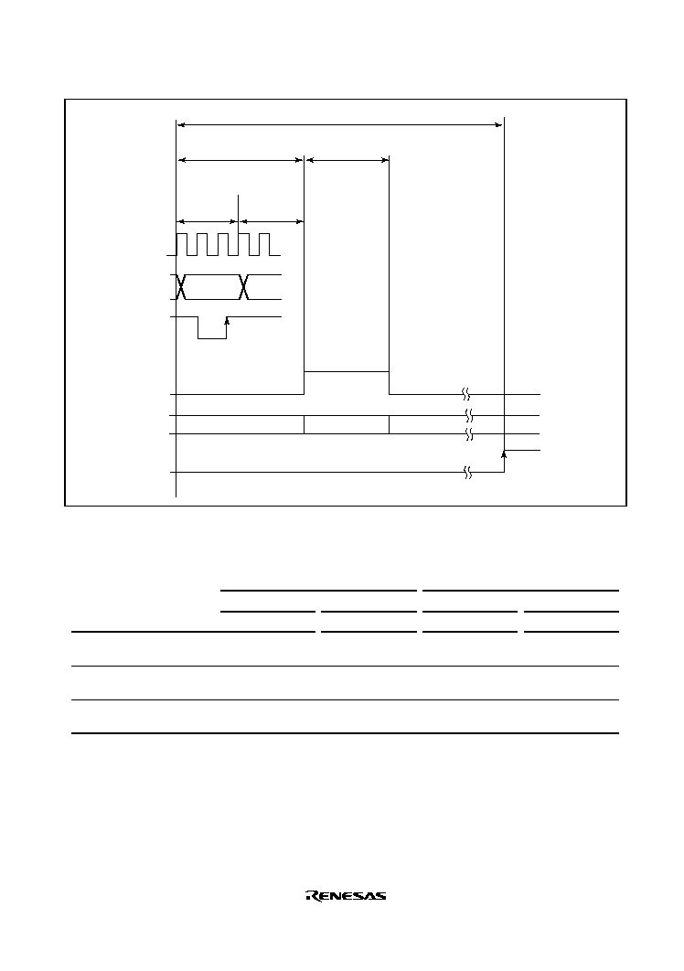
Rev. 2.0, 09/02, page 473 of 732
P
A/D converter
A/D conversion
A/D conversion start
delay time(t
D
)
A/D conversion time (t
CONV
)
Analog input
sampling time(t
SPL
)
ADST write timing
End of A/D conversion
ADF
Address
ADCSR
write
cycle
Internal write
signal
Analog input
sampling time
Idle state
Sample-and-hold
Figure 15.2 A/D Conversion Timing
Table 15.3 A/D Conversion Time (Single Mode)
CKS1 = 0
CKS1 = 1
CKS0 = 0
CKS0 = 1
CKS0 = 0
CKS0 = 1
Item
Symbol
Min
Typ
Max
Min
Typ
Max
Min
Typ
Max
Min
Typ
Max
A/D conversion
start delay
t
D
31
--
62
15
--
30
7
--
14
3
--
6
Input sampling
time
t
SPL
--
256
--
--
128
--
--
64
--
--
32
--
A/D conversion
time
t
CONV
1024 --
1055
515
--
530
259
--
266
131
--
134
Note:
All values represent the number of states for P
.
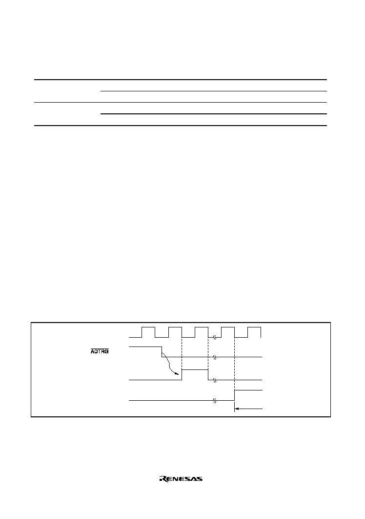
Rev. 2.0, 09/02, page 474 of 732
Table 15.4 A/D Conversion Time (Scan Mode)
CKS1
CKS0
Conversion Time (State)
0
1024 (Fixed)
0
1
512 (Fixed)
0
256 (Fixed)
1
1
128 (Fixed)
15.4.5
A/D Converter Activation by MTU
The A/D converter can be independently activated by an A/D conversion request from the interval
timer of the MTU.
To activate the A/D converter by the MTU, set the A/D trigger select register (ADTSR). After this
register setting has been made, the ADST bit in ADCR is automatically set to 1 when an A/D
conversion request from the interval timer of the MTU occurs. The timing from setting of the
ADST bit until the start of A/D conversion is the same as when 1 is written to the ADST bit by
software.
15.4.6
External Trigger Input Timing
A/D conversion can be externally triggered. When the TRGS1 and TRGS0 bits are set to 00 or 01
in ADTSR, external trigger input is enabled at the
ADTRG pin. A falling edge of the ADTRG pin
sets the ADST bit to 1 in ADCR, starting A/D conversion. Other operations, in both single and
scan modes, are the same as when the ADST bit has been set to 1 by software. Figure 15.3 shows
the timing.
CK
External trigger
signal
ADST
A/D conversion
Figure 15.3 External Trigger Input Timing

Rev. 2.0, 09/02, page 475 of 732
15.5
Interrupt Sources and DTC, DMAC Transfer Requests
The A/D converter generates an A/D conversion end interrupt (ADI) upon the completion of A/D
conversion. ADI interrupt requests are enabled when the ADIE bit is set to 1 while the ADF bit in
ADCSR is set to 1 after A/D conversion is completed. The data transfer controller (DTC) or the
direct memory access controller (DMAC) can be activated by an ADI interrupt. Having the
converted data read by the DTC or the DMAC in response to an ADI interrupt enables continuous
conversion to be achieved without imposing a load on software.
When the DTC or the DMAC is activated by an ADI interrupt, the ADF bit in ADCSR is
automatically cleared when data is transferred by the DTC or the DMAC.
Table 15.5 A/D Converter Interrupt Source
Name
Interrupt Source
Interrupt Source Flag DTC Activation DMAC Activation
ADI0
A/D0 conversion completed ADF in ADCSR_0
Possible
Impossible
ADI1
A/D1 conversion completed ADF in ADCSR_1
Possible
Possible
15.6
Definitions of A/D Conversion Accuracy
This LSI's A/D conversion accuracy definitions are given below.
∑
Resolution
The number of A/D converter digital output codes
∑
Quantization error
The deviation inherent in the A/D converter, given by 1/2 LSB (see figure 15.4).
∑
Offset error
The deviation of the analog input voltage value from the ideal A/D conversion characteristic
when the digital output changes from the minimum voltage value B'0000000000 (H'00) to
B'0000000001 (H'01) (see figure 15.5).
∑
Full-scale error
The deviation of the analog input voltage value from the ideal A/D conversion characteristic
when the digital output changes from B'1111111110 (H'3FE) to B'1111111111 (H'3FF) (see
figure 15.5).
∑
Nonlinearity error
The error with respect to the ideal A/D conversion characteristic between zero voltage and full-
scale voltage. Does not include offset error, full-scale error, or quantization error (see figure
15.5).
∑
Absolute accuracy
The deviation between the digital value and the analog input value. Includes offset error, full-
scale error, quantization error, and nonlinearity error.
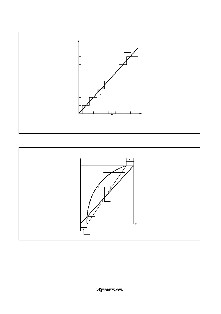
Rev. 2.0, 09/02, page 476 of 732
111
110
101
100
011
010
001
000
1
1024
2
1024
1022
1024
1023
1024
FS
Quantization error
Digital output
Ideal A/D conversion
characteristic
Analog
input voltage
Figure 15.4 Definitions of A/D Conversion Accuracy
FS
Digital output
Ideal A/D conversion
characteristic
Nonlinearity
error
Analog
input voltage
Offset error
Actual A/D conversion
characteristic
Full-scale error
Figure 15.5 Definitions of A/D Conversion Accuracy
Rev. 2.0, 09/02, page 477 of 732
15.7
Usage Notes
15.7.1
Module Standby Mode Setting
Operation of the A/D converter can be disabled or enabled using the module standby control
register. The initial setting is for operation of the A/D converter to be halted. Register access is
enabled by clearing module standby mode. For details, refer to section 24, Power-Down Modes.
15.7.2
Permissible Signal Source Impedance
This LSI's analog input is designed such that conversion accuracy is guaranteed for an input signal
for which the signal source impedance is 1 k
or less. This specification is provided to enable the
A/D converter's sample-and-hold circuit input capacitance to be charged within the sampling time;
if the sensor output impedance exceeds 1 k
, charging may be insufficient and it may not be
possible to guarantee A/D conversion accuracy. With a large capacitance provided externally for
A/D conversion in single mode, the input impedance will essentially comprise only the internal
input resistance of 10 k
, and the signal source impedance is ignored. However, as a low-pass
filter effect is obtained in this case, it may not be possible to follow a high speed switching analog
signal (e.g., 5 mV/
µ
s or greater) (see figure 15.6). When converting a high-speed analog signal or
performing conversion in scan mode, a low-impedance buffer should be inserted.
15.7.3
Influences on Absolute Accuracy
Adding capacitance results in coupling with GND, and therefore noise in GND may adversely
affect absolute accuracy. Be sure to make the connection to an electrically stable GND such as
AVss.
Care is also required to insure that filter circuits do not interfere in the accuracy by the digital
signals on the printed circuit board (i.e, acting as antennas).
20 pF
10 k
C
in
=
20 pF
Sensor output
impedance of
up to 1 k
This LSI
Low-pass
filter
C = 0.1 F
Sensor input
A/D converter
equivalent circuit
Figure 15.6 Example of Analog Input Circuit

Rev. 2.0, 09/02, page 478 of 732
15.7.4
Range of Analog Power Supply and Other Pin Settings
If the conditions below are not met, the reliability of the device may be adversely affected.
∑
Analog input voltage range
The voltage applied to analog input pin ANn (VANn) during A/D conversion should be in the
range AVss
VANn
AVcc.
∑
Relationship between AVcc, Avss and Vcc, Vss
The Relationship between AVcc, AVss and Vcc, Vss should be AVcc = Vcc
±
0.3V and Avss
= Vss. If the A/D converter is not used, this relationship should be AVcc = Vcc and Avss =
Vss.
∑
Setting range of AVref input voltage (only for SH7145)
Set the AVref pin input voltage as AVref
AVcc. If the A/D converter is not used, set the
AVref pin as AVref = AVcc.
15.7.5
Notes on Board Design
In board design, digital circuitry and analog circuitry should be as mutually isolated as possible,
and layout in which digital circuit signal lines and analog circuit signal lines cross or are in close
proximity should be avoided as far as possible. Failure to do so may result in incorrect operation
of the analog circuitry due to inductance, adversely affecting A/D conversion values. Also, digital
circuitry must be isolated from the analog input signals (AN0 to AN7), and analog power supply
(AVcc) by the analog ground (AVss). Also, the analog ground (AVss) should be connected at one
point to a stable digital ground (Vss) on the board.
15.7.6
Notes on Noise Countermeasures
A protection circuit should be connected in order to prevent damage due to abnormal voltage, such
as an excessive surge at the analog input pins (AN0 to AN7), to AVcc and AVss, as shown in
figure 15.7. Also, the bypass capacitors connected to AVcc and the filter capacitor connected to
AN0 to AN7 must be connected to AVss.
If a filter capacitor is connected, the input currents at the analog input pins (AN0 to AN7) are
averaged, and so an error may arise. Also, when A/D conversion is performed frequently, as in
scan mode, if the current charged and discharged by the capacitance of the sample-and-hold circuit
in the A/D converter exceeds the current input via the input impedance (R
in
), an error will arise in
the analog input pin voltage. Careful consideration is therefore required when deciding circuit
constants.
Rev. 2.0, 09/02, page 479 of 732
AVCC
AVref
*
1
AN0 to AN7
AVSS
*
1
R
in
*
2
100
0.1 µF
0.01 µF
10 µF
Notes: Values are reference values.
*
1
*
2 R
in
: Input impedance
Figure 15.7 Example of Analog Input Protection Circuit
Table 15.6 Analog Pin Specifications
Item
Min
Max
Unit
Analog input capacitance
--
20
pF
Permissible signal source impedance
--
1
k

Rev. 2.0, 09/02, page 480 of 732
TIMCMT0A_000220020700
Rev. 2.0, 09/02, page 481 of 732
Section 16 Compare Match Timer (CMT)
This LSI has an on-chip compare match timer (CMT) comprising two 16-bit timer channels. The
CMT has 16-bit counters and can generate interrupts at specified intervals.
16.1
Features
The CMT has the following features:
∑
Four kinds of counter input clock can be selected
One of four internal clocks (P
/8, P
/32, P
/128, P
/512) can be selected independently
for each channel.
∑
Interrupt sources
A compare match interrupt can be requested independently for each channel.
∑
Module standby mode can be set
Figure 16.1 shows a block diagram of the CMT.
Control circuit
Clock selection
Module bus
Control circuit
Clock selection
CMI0
CMI1
P
/8
P
/32
P
/128
P
/512
P
/8
P
/32
P
/128
P
/512
Bus
interface
Internal bus
Legend:
CMSTR: Compare match timer start register
CMCSR: Compare match timer control/status register
CMCOR: Compare match timer constant register
CMCNT: Compare match timer counter
CMI:
Compare match interrupt
Comparator
CMSTR
CMT
CMCSR_0
CMCOR_0
Comparator
CMCNT_0
CMCSR_1
CMCOR_1
CMCNT_1
Figure 16.1 CMT Block Diagram

Rev. 2.0, 09/02, page 482 of 732
16.2
Register Descriptions
The CMT has the following registers. For details on register addresses and register states during
each processing, refer to section 25, List of Registers.
∑
Compare match timer start register (CMSTR)
∑
Compare match timer control/status register_0 (CMCSR_0)
∑
Compare match timer counter_0 (CMCNT_0)
∑
Compare match timer constant register_0 (CMCOR_0)
∑
Compare match timer control/status register_1 (CMCSR_1)
∑
Compare match timer counter_1 (CMCNT_1)
∑
Compare match timer constant register_1 (CMCOR_1)
16.2.1
Compare Match Timer Start Register (CMSTR)
The compare match timer start register (CMSTR) is a 16-bit register that selects whether to
operate or halt the channel 0 and channel 1 counters (CMCNT).
Bit
Bit Name Initial Value
R/W
Description
15 to 2
All 0
R
Reserved
These bits always read 0. The write value should
always be 0.
1
STR1
0
R/W
Count Start 1
This bit selects whether to operate or halt compare
match timer counter_1. (CMCNT_1)
0: CMCNT_1 count operation halted
1: CMCNT_1 count operation
0
STR0
0
R/W
Count Start 0
This bit selects whether to operate or halt compare
match timer counter_0. (CMCNT_0)
0: CMCNT_0 count operation halted
1: CMCNT_0 count operation

Rev. 2.0, 09/02, page 483 of 732
16.2.2
Compare Match Timer Control/Status Register 0 and 1(CMCSR0, 1)
The compare match timer control/status register (CMCSR) is a 16-bit register that indicates the
occurrence of compare matches, sets the enable/disable status of interrupts, and establishes the
clock used for incrementation. It is initialized to H'0000 by a power-on reset and in the standby
modes.
Bit
Bit Name Initial Value
R/W
Description
15 to 8
All 0
R
Reserved
These bits always read 0. The write value should
always be 0.
7
CMF
0
R/(W)
*
Compare Match Flag
This flag indicates whether or not the CMCNT and
CMCOR values have matched.
0: CMCNT and CMCOR values have not matched
[Clearing condition]
∑
Write 0 to CMF after reading 1 from it
1: CMCNT and CMCOR values have matched
6
CMIE
0
R/W
Compare Match Interrupt Enable
This bit selects whether to enable or disable a
compare match interrupt (CMI) when the CMCNT and
CMCOR values have matched (CMF = 1).
0: Compare match interrupt (CMI) disabled
1: Compare match interrupt (CMI) enabled
5 to 2
All 0
R
Reserved
These bits always read 0. The write value should
always be 0.
1
0
CKS1
CKS0
0
0
R/W
R/W
These bits select the clock input to CMCNT from
among the four internal clocks obtained by dividing
the peripheral clock (P
). When the STR bit of
CMSTR is set to 1, CMCNT begins incrementing with
the clock selected by CKS1 and CKS0.
00: P
/8
01: P
/32
10: P
/128
11: P
/512
Note:
*
Only 0 can be written, for flag clearing.
Rev. 2.0, 09/02, page 484 of 732
16.2.3
Compare Match Timer Counter_0 and 1 (CMCNT_0, 1)
The compare match timer counter (CMCNT) is a 16-bit register used as an up-counter for
generating interrupt requests.
The initial value of CMCNT is H
0000.
16.2.4
Compare Match Timer Constant Register_0 and 1 (CMCOR_0, 1)
The compare match timer constant register (CMCOR) is a 16-bit register that sets the period for
compare match with CMCNT.
The initial value of CMCOR is H
FFFF.
16.3
Operation
16.3.1
Compare Match Counter Operation
When an internal clock is selected with the CKS1, CKS0 bits of the CMCSR register and the STR
bit of CMSTR is set to 1, CMCNT begins incrementing with the selected clock. When the
CMCNT counter value matches that of the compare match constant register (CMCOR), the
CMCNT counter is cleared to H'0000 and the CMF flag of the CMCSR register is set to 1. If the
CMIE bit of the CMCSR register is set to 1 at this time, a compare match interrupt (CMI) is
requested. The CMCNT counter begins counting up again from H'0000.
Figure 16.2 shows the compare match counter operation.
CMCNT value
CMCOR
H'0000
Counter cleared by CMCOR
compare match
Time
Figure 16.2 Counter Operation
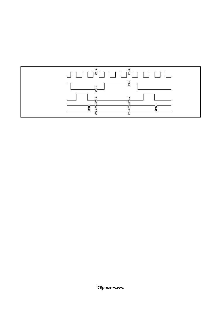
Rev. 2.0, 09/02, page 485 of 732
16.3.2
CMCNT Count Timing
One of four clocks (P
/8, P
/32, P
/128, P
/512) obtained by dividing the peripheral clock (P
)
can be selected by the CKS1 and CKS0 bits of CMCSR. Figure 16.3 shows the CMCNT count
timing.
P
Internal
clock
CMCNT
input clock
CMCNT
N-1
N
N+1
Figure 16.3 Count Timing
16.4
Interrupts
16.4.1
Interrupt Sources and DTC Activation
The CMT has a compare match interrupt for each channel, with independent vector addresses
allocated to each of them. The corresponding interrupt request is output when interrupt request
flag CMF is set to 1 and interrupt enable bit CMIE has also been set to 1.
When activating CPU interrupts by interrupt request, the priority between the channels can be
changed by means of interrupt controller settings. See section 6, Interrupt Controller, for details.
The data transfer controller (DTC) can be activated by an interrupt request. In this case, the
priority between channels is fixed. See section 8, Data Transfer Controller, for details.
16.4.2
Compare Match Flag Set Timing
The CMF bit of the CMCSR register is set to 1 by the compare match signal generated when the
CMCOR register and the CMCNT counter match. The compare match signal is generated upon
the final state of the match (timing at which the CMCNT counter matching count value is
updated). Consequently, after the CMCOR register and the CMCNT counter match, a compare
match signal will not be generated until a CMCNT counter input clock occurs. Figure 16.4 shows
the CMF bit set timing.
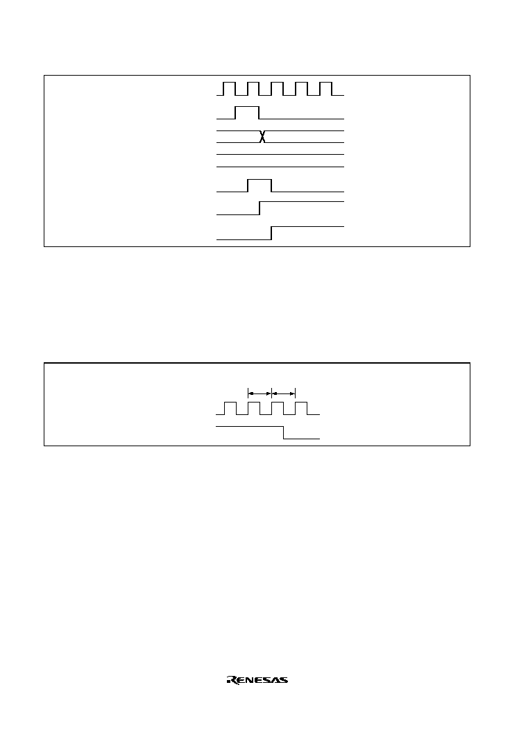
Rev. 2.0, 09/02, page 486 of 732
CMCNT
input clock
CMCNT
CMCOR
N
0
N
Compare
match signal
CMF
CMI
P
Figure 16.4 CMF Set Timing
16.4.3
Compare Match Flag Clear Timing
The CMF bit of the CMCSR register is cleared by writing a 0 to it after reading a 1 or the clearing
signal after the DTC transfer. Figure 16.5 shows the timing when the CMF bit is cleared by the
CPU.
T1
T2
CMCSR write cycle
P
CMF
Figure 16.5 Timing of CMF Clear by the CPU
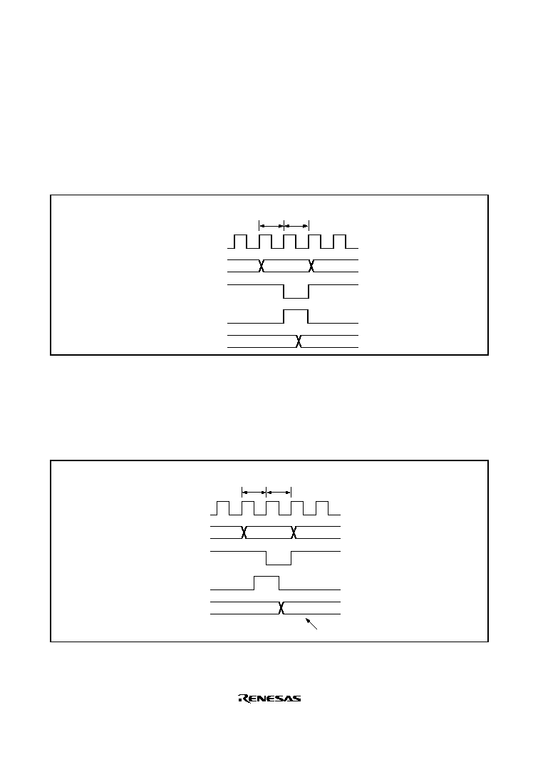
Rev. 2.0, 09/02, page 487 of 732
16.5
Usage Notes
16.5.1
Contention between CMCNT Write and Compare Match
If a compare match signal is generated during the T2 state of the CMCNT counter write cycle, the
CMCNT counter clear has priority, so the write to the CMCNT counter is not performed. Figure
16.6 shows the timing.
P
T1
T2
Address
CMCNT
Internal
write signal
CMCNT
N
H' 0000
Compare
match signal
CMCNT write cycle
Figure 16.6 CMCNT Write and Compare Match Contention
16.5.2
Contention between CMCNT Word Write and Counter Incrementation
If an increment occurs during the T2 state of the CMCNT counter word write cycle, the counter
write has priority, so no increment occurs. Figure 16.7 shows the timing.
P
T1
T2
Address
CMCNT
Internal write
signal
CMCNT
N
M
CMCNT write data
CMCNT
input clock
CMCNT write cycle
Figure 16.7 CMCNT Word Write and Increment Contention
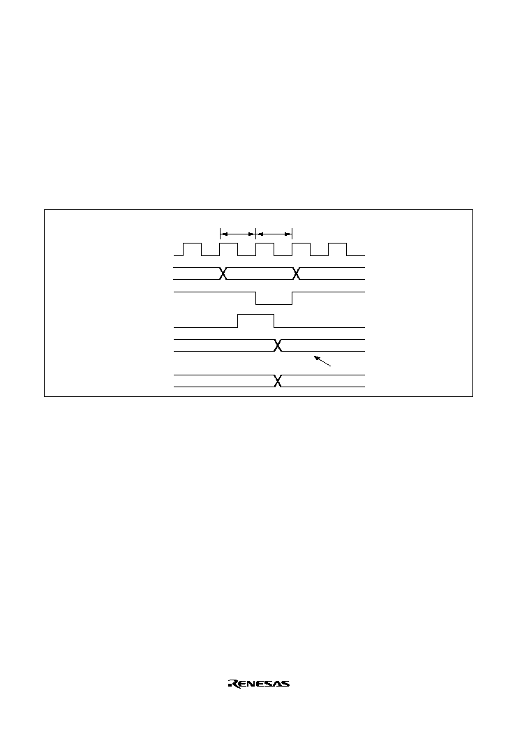
Rev. 2.0, 09/02, page 488 of 732
16.5.3
Contention between CMCNT Byte Write and Counter Incrementation
If an increment occurs during the T2 state of the CMCNT byte write cycle, the counter write has
priority, so no increment of the write data results on the side on which the write was performed.
The byte data on the side on which writing was not performed is also not incremented, so the
contents are those before the write.
Figure 16.8 shows the timing when an increment occurs during the T2 state of the CMCNT
(Upper byte) write cycle.
P
T1
T2
Address
CMCNT (Upper byte)
Internal write
signal
CMCNT
(Upper byte)
N
M
CMCNT
(Lower byte)
X
X
CMCNT write data
CMCNT input
clock
CMCNT write cycle
Figure 16.8 CMCNT Byte Write and Increment Contention

Rev. 2.0, 09/02, page 489 of 732
Section 17 Pin Function Controller (PFC)
The pin function controller (PFC) is composed of registers that are used to select the
functions of multiplexed pins and assign pins to be inputs or outputs. Tables 17.1 to 17.12
list the multiplexed pins of this LSI.
Tables 17.13 and 17.14 list the pin functions in each operating mode.
Table 17.1 SH7144 Multiplexed Pins (Port A)
Port
Function 1
(Related Module)
Function 2
(Related Module)
Function 3
(Related Module)
Function 4
(Related Module)
A
PA0 I/O (port)
RXD0 input (SCI)
PA1 I/O (port)
TXD0 output (SCI)
PA2 I/O (port)
SCK0 I/O (SCI)
DREQ0
input (DMAC)
IRQ0
input (INTC)
PA3 I/O (port)
RXD1 input (SCI)
PA4 I/O (port)
TXD1 output (SCI)
PA5 I/O (port)
SCK1 I/O (SCI)
DREQ1
input (DMAC)
IRQ1
input (INTC)
PA6 I/O (port)
TCLKA input (MTU)
CS2
output (BSC)
PA7 I/O (port)
TCLKB input (MTU)
CS3
output (BSC)
PA8 I/O (port)
TCLKC input (MTU)
IRQ2
input (INTC)
PA9 I/O (port)
TCLKD input (MTU)
IRQ3
input (INTC)
PA10 I/O (port)
CS0
output (BSC)
PA11 I/O (port)
CS1
output (BSC)
PA12 I/O (port)
WRL
output (BSC)
PA13 I/O (port)
WRH
output (BSC)
PA14 I/O (port)
RD
output (BSC)
PA15 I/O (port)
CK output (CPG)

Rev. 2.0, 09/02, page 490 of 732
Table 17.2 SH7144 Multiplexed Pins (Port B)
Port
Function 1
(Related Module)
Function 2
(Related Module)
Function 3
(Related Module)
Function 4
(Related Module)
Function 5
(Related Module)
B
PB0 I/O (port)
A16 output (BSC)
PB1 I/O (port)
A17 output (BSC)
PB2 I/O (port)
IRQ0
input (INTC)
POE0
input (port)
SCL0 I/O (IIC)
PB3 I/O (port)
IRQ1
input (INTC)
POE1
input (port)
SDA0 I/O (IIC)
PB4 I/O (port)
IRQ2
input (INTC)
POE2
input (port)
PB5 I/O (port)
IRQ3
input (INTC)
POE3
input (port)
PB6 I/O (port)
IRQ4
input (INTC)
A18 output (BSC)
BACK
output (BSC)
PB7 I/O (port)
IRQ5
input (INTC)
A19 output (BSC)
BREQ
input (BSC)
PB8 I/O (port)
IRQ6
input (INTC)
A20 output (BSC)
WAIT
input (BSC)
PB9 I/O (port)
IRQ7
input (INTC)
A21 output (BSC)
ADTRG
input (A/D)
Table 17.3 SH7144 Multiplexed Pins (Port C)
Port
Function 1
(Related Module)
Function 2
(Related Module)
Function 3
(Related Module)
Function 4
(Related Module)
C
PC0 I/O (port)
A0 output (BSC)
PC1 I/O (port)
A1 output (BSC)
PC2 I/O (port)
A2 output (BSC)
PC3 I/O (port)
A3 output (BSC)
PC4 I/O (port)
A4 output (BSC)
PC5 I/O (port)
A5 output (BSC)
PC6 I/O (port)
A6 output (BSC)
PC7 I/O (port)
A7 output (BSC)
PC8 I/O (port)
A8 output (BSC)
PC9 I/O (port)
A9 output (BSC)
PC10 I/O (port)
A10 output (BSC)
PC11 I/O (port)
A11 output (BSC)
PC12 I/O (port)
A12 output (BSC)
PC13 I/O (port)
A13 output (BSC)
PC14 I/O (port)
A14 output (BSC)
PC15 I/O (port)
A15 output (BSC)

Rev. 2.0, 09/02, page 491 of 732
Table 17.4 SH7144 Multiplexed Pins (Port D)
Port
Function 1
(Related Module)
Function 2
(Related Module)
Function 3
(Related Module)
Function 4
(Related Module)
D
PD0 I/O (port)
D0 I/O (BSC)
PD1 I/O (port)
D1 I/O (BSC)
PD2 I/O (port)
D2 I/O (BSC)
PD3 I/O (port)
D3 I/O (BSC)
PD4 I/O (port)
D4 I/O (BSC)
PD5 I/O (port)
D5 I/O (BSC)
PD6 I/O (port)
D6 I/O (BSC)
PD7 I/O (port)
D7 I/O (BSC)
PD8 I/O (port)
D8 I/O (BSC)
AUDATA0 I/O (AUD)
*
PD9 I/O (port)
D9 I/O (BSC)
AUDATA1 I/O (AUD)
*
PD10 I/O (port)
D10 I/O (BSC)
AUDATA2 I/O (AUD)
*
PD11 I/O (port)
D11 I/O (BSC)
AUDATA3 I/O (AUD)
*
PD12 I/O (port)
D12 I/O (BSC)
AUDRST
input (AUD)
*
PD13 I/O (port)
D13 I/O (BSC)
AUDMD input (AUD)
*
PD14 I/O (port)
D14 I/O (BSC)
AUDCK I/O (AUD)
*
PD15 I/O (port)
D15 I/O (BSC)
AUDSYNC
I/O (AUD)
*
Note:
*
F-ZTAT only.

Rev. 2.0, 09/02, page 492 of 732
Table 17.5 SH7144 Multiplexed Pins (Port E)
Port
Function 1
(Related Module)
Function 2
(Related Module)
Function 3
(Related Module)
Function 4
(Related Module)
E
PE0 I/O port
TIOC0A I/O (MTU)
DREQ0
input (DMAC)
TMS input (H-UDI)
*
PE1 I/O port
TIOC0B I/O (MTU)
DRAK0 output (DMAC)
TRST
input (H-UDI)
*
PE2 I/O port
TIOC0C I/O (MTU)
DREQ1
input (DMAC)
TDI input (H-UDI)
*
PE3 I/O port
TIOC0D I/O (MTU)
DRAK1 output (DMAC)
TDO output (H-UDI)
*
PE4 I/O port
TIOC1A I/O (MTU)
RXD3 input (SCI)
TCK input (H-UDI)
*
PE5 I/O port
TIOC1B I/O (MTU)
TXD3 output (SCI)
PE6 I/O port
TIOC2A I/O (MTU)
SCK3 I/O (SCI)
PE7 I/O port
TIOC2B I/O (MTU)
RXD2 input (SCI)
PE8 I/O port
TIOC3A I/O (MTU)
SCK2 I/O (SCI)
PE9 I/O port
TIOC3B I/O (MTU)
SCK3 I/O (SCI)
PE10 I/O port
TIOC3C I/O (MTU)
TXD2 output (SCI)
PE11 I/O port
TIOC3D I/O (MTU)
RXD3 input (SCI)
PE12 I/O port
TIOC4A I/O (MTU)
TXD3 output (SCI)
PE13 I/O port
TIOC4B I/O (MTU)
MRES
input (INTC)
PE14 I/O port
TIOC4C I/O (MTU)
DACK0 output (DMAC)
PE15 I/O port
TIOC4D I/O (MTU)
DACK1 output (DMAC)
IRQOUT
output (INTC)
Note:
*
F-ZTAT only.
Table 17.6 SH7144 Multiplexed Pins (Port F)
Port
Function 1
(Related Module)
Function 2
(Related Module)
Function 3
(Related Module)
Function 4
(Related Module)
F
PF0 input (port)
AN0 input (A/D)
PF1 input (port)
AN1 input (A/D)
PF2input (port)
AN2 input (A/D)
PF3 input (port)
AN3 input (A/D)
PF4 input (port)
AN4 input (A/D)
PF5 input (port)
AN5 input (A/D)
PF6 input (port)
AN6 input (A/D)
PF7 input (port)
AN7 input (A/D)

Rev. 2.0, 09/02, page 493 of 732
Table 17.7 SH7145 Multiplexed Pins (Port A)
Port
Function 1
(Related Module)
Function 2
(Related Module)
Function 3
(Related Module)
Function 4
(Related Module)
A
PA0 I/O (port)
RXD0 input (SCI)
PA1 I/O (port)
TXD0 output (SCI)
PA2 I/O (port)
SCK0 I/O (SCI)
DREQ0
input (DMAC)
IRQ0
input (INTC)
PA3 I/O (port)
RXD1 input (SCI)
PA4 I/O (port)
TXD1 output (SCI)
PA5 I/O (port)
SCK1 I/O (SCI)
DREQ1
input (DMAC)
IRQ1
input (INTC)
PA6 I/O (port)
TCLKA input (MTU)
CS2
output (BSC)
PA7 I/O (port)
TCLKB input (MTU)
CS3
output (BSC)
PA8 I/O (port)
TCLKC input (MTU)
IRQ2
input (INTC)
PA9 I/O (port)
TCLKD input (MTU)
IRQ3
input (INTC)
PA10 I/O (port)
CS0
output (BSC)
PA11 I/O (port)
CS1
output (BSC)
PA12 I/O (port)
WRL
output (BSC)
PA13 I/O (port)
WRH
output (BSC)
PA14 I/O (port)
RD
output (BSC)
PA15 I/O (port)
CK output (CPG)
PA16 I/O (port)
AUDSYNC
I/O (AUD)
*
PA17 I/O (port)
WAIT
input (BSC)
PA18 I/O (port)
BREQ
input (BSC)
DRAK0 output (DMAC)
PA19 I/O (port)
BACK
output (BSC)
DRAK1 output (DMAC)
PA20 I/O (port)
PA21 I/O (port)
PA22 I/O (port)
WRHL
output (BSC)
PA23 I/O (port)
WRHH
output (BSC)
Note:
*
F-ZTAT only.

Rev. 2.0, 09/02, page 494 of 732
Table 17.8 SH7145 Multiplexed Pins (Port B)
Port
Function 1
(Related Module)
Function 2
(Related Module)
Function 3
(Related Module)
Function 4
(Related Module)
Function 5
(Related Module)
B
PB0 I/O (port)
A16 output (BSC)
PB1 I/O (port)
A17 output (BSC)
PB2 I/O (port)
IRQ0
input (INTC)
POE0
input (port)
SCL0 I/O (IIC)
PB3 I/O (port)
IRQ1
input (INTC)
POE1
input (port)
SDA0 I/O (IIC)
PB4 I/O (port)
IRQ2
input (INTC)
POE2
input (port)
PB5 I/O (port)
IRQ3
input (INTC)
POE3
input (port)
PB6 I/O (port)
IRQ4
input (INTC)
A18 output (BSC)
BACK
output (BSC)
PB7 I/O (port)
IRQ5
input (INTC)
A19 output (BSC)
BREQ
input (BSC)
PB8 I/O (port)
IRQ6
input (INTC)
A20 output (BSC)
WAIT
input (BSC)
PB9 I/O (port)
IRQ7
input (INTC)
A21 output (BSC)
ADTRG
input (A/D)
Table 17.9 SH7145 Multiplexed Pins (Port C)
Port
Function 1 (Related
Module)
Function 2 (Related
Module)
Function 3 (Related
Module)
Function 4 (Related
Module)
C
PC0 I/O (port)
A0 output (BSC)
PC1 I/O (port)
A1 output (BSC)
PC2 I/O (port)
A2 output (BSC)
PC3 I/O (port)
A3 output (BSC)
PC4 I/O (port)
A4 output (BSC)
PC5 I/O (port)
A5 output (BSC)
PC6 I/O (port)
A6 output (BSC)
PC7 I/O (port)
A7 output (BSC)
PC8 I/O (port)
A8 output (BSC)
PC9 I/O (port)
A9 output (BSC)
PC10 I/O (port)
A10 output (BSC)
PC11 I/O (port)
A11 output (BSC)
PC12 I/O (port)
A12 output (BSC)
PC13 I/O (port)
A13 output (BSC)
PC14 I/O (port)
A14 output (BSC)
PC15 I/O (port)
A15 output (BSC)

Rev. 2.0, 09/02, page 495 of 732
Table 17.10 SH7145 Multiplexed Pins (Port D)
Port
Function 1
(Related Module)
Function 2
(Related Module)
Function 3
(Related Module)
Function 4
(Related Module)
D
PD0 I/O (port)
D0 I/O (BSC)
PD1 I/O (port)
D1 I/O (BSC)
PD2 I/O (port)
D2 I/O (BSC)
PD3 I/O (port)
D3 I/O (BSC)
PD4 I/O (port)
D4 I/O (BSC)
PD5 I/O (port)
D5 I/O (BSC)
PD6 I/O (port)
D6 I/O (BSC)
PD7 I/O (port)
D7 I/O (BSC)
PD8 I/O (port)
D8 I/O (BSC)
PD9 I/O (port)
D9 I/O (BSC)
PD10 I/O (port)
D10 I/O (BSC)
PD11 I/O (port)
D11 I/O (BSC)
PD12 I/O (port)
D12 I/O (BSC)
PD13 I/O (port)
D13 I/O (BSC)
PD14 I/O (port)
D14 I/O (BSC)
PD15 I/O (port)
D15 I/O (BSC)
PD16 I/O (port)
D16 I/O (BSC)
IRQ0
input (INTC)
AUDATA0 I/O (AUD)
*
PD17 I/O (port)
D17 I/O (BSC)
IRQ1
input (INTC)
AUDATA1 I/O (AUD)
*
PD18 I/O (port)
D18 I/O (BSC)
IRQ2
input (INTC)
AUDATA2 I/O (AUD)
*
PD19 I/O (port)
D19 I/O (BSC)
IRQ3
input (INTC)
AUDATA3 I/O (AUD)
*
PD20 I/O (port)
D20 I/O (BSC)
IRQ4
input (INTC)
AUDRST
input (AUD)
*
PD21 I/O (port)
D21 I/O (BSC)
IRQ5
input (INTC)
AUDMD input (AUD)
*
PD22 I/O (port)
D22 I/O (BSC)
IRQ6
input (INTC)
AUDCK I/O (AUD)
*
PD23 I/O (port)
D23 I/O (BSC)
IRQ7
input (INTC)
AUDSYNC
I/O (AUD)
*
PD24 I/O (port)
D24 I/O (BSC)
DREQ0
input (DMAC)
PD25 I/O (port)
D25 I/O (BSC)
DREQ1
input (DMAC)
PD26 I/O (port)
D26 I/O (BSC)
DACK0 output (DMAC)
PD27 I/O (port)
D27 I/O (BSC)
DACK1 output (DMAC)
PD28 I/O (port)
D28 I/O (BSC)
CS2
output (BSC)
PD29 I/O (port)
D29 I/O (BSC)
CS3
output (BSC)
PD30 I/O (port)
D30 I/O (BSC)
IRQOUT
output (INTC)
PD31 I/O (port)
D31 I/O (BSC)
ADTRG
input (A/D)
Note:
*
F-ZTAT only.

Rev. 2.0, 09/02, page 496 of 732
Table 17.11 SH7145 Multiplexed Pins (Port E)
Port
Function 1
(Related Module)
Function 2
(Related Module)
Function 3
(Related Module)
Function 4
(Related Module)
E
PE0 I/O (port)
TIOC0A I/O (MTU)
DREQ0
input (DMAC)
AUDCK I/O (AUD)
*
PE1 I/O (port)
TIOC0B I/O (MTU)
DACK0 output (DMAC)
AUDMD input (AUD)
*
PE2 I/O (port)
TIOC0C I/O (MTU)
DREQ1
input (DMAC)
AUDRST
input (AUD)
*
PE3 I/O (port)
TIOC0D I/O (MTU)
DACK1 output (DMAC)
AUDATA3 I/O (AUD)
*
PE4 I/O (port)
TIOC1A I/O (MTU)
RXD3 input (SCI)
AUDATA2 I/O (AUD)
*
PE5 I/O (port)
TIOC1B I/O (MTU)
TXD3 output (SCI)
AUDATA1 I/O (AUD)
*
PE6 I/O (port)
TIOC2A I/O (MTU)
SCK3 I/O (SCI)
AUDATA0 I/O (AUD)
*
PE7 I/O (port)
TIOC2B I/O (MTU)
RXD2 input (SCI)
PE8 I/O (port)
TIOC3A I/O (MTU)
SCK2 I/O (SCI)
TMS input (H-UDI)
*
PE9 I/O (port)
TIOC3B I/O (MTU)
TRST
input (H-UDI)
*
SCK3 I/O (SCI)
PE10 I/O (port)
TIOC3C I/O (MTU)
TXD2 output (SCI)
TDI input (H-UDI)
*
PE11 I/O (port)
TIOC3D I/O (MTU)
TDO output (H-UDI)
*
RXD3 input (SCI)
PE12 I/O (port)
TIOC4A I/O (MTU)
TCK input (H-UDI)
*
TXD3 output (SCI)
PE13 I/O (port)
TIOC4B I/O (MTU)
MRES
input (INTC)
PE14 I/O (port)
TIOC4C I/O (MTU)
DACK0 output (DMAC)
PE15 I/O (port)
TIOC4D I/O (MTU)
DACK1 output (DMAC)
IRQOUT
output (INTC)
Note:
*
F-ZTAT only.
Table 17.12 SH7145 Multiplexed Pins (Port F)
Port
Function 1
(Related Module)
Function 2
(Related Module)
Function 3
(Related Module)
Function 4
(Related Module)
F
PF0 input (port)
AN0 input (A/D)
PF1 input (port)
AN1 input (A/D)
PF2 input (port)
AN2 input (A/D)
PF3 input (port)
AN3 input (A/D)
PF4 input (port)
AN4 input (A/D)
PF5 input (port)
AN5 input (A/D)
PF6 input (port)
AN6 input (A/D)
PF7 input (port)
AN7 input (A/D)

Rev. 2.0, 09/02, page 497 of 732
Table 17.13 SH7144 Pin Functions in Each Mode (1)
Pin Name
Pin No.
On-Chip ROM Disabled (MCU mode 0)
On-Chip ROM Disabled (MCU mode 1)
SH7144
Initial Function
PFC Selected Function
Possibilities
Initial Function
PFC Selected Function
Possibilities
21, 37, 65,
103
Vcc
Vcc
Vcc
Vcc
3, 23, 39,
55, 61, 71,
90, 101,
109
Vss
Vss
Vss
Vss
100
AVcc
AVcc
AVcc
AVcc
97
AVss
AVss
AVss
AVss
80
PLLVcc
PLLVcc
PLLVcc
PLLVcc
81
PLLCAP
PLLCAP
PLLCAP
PLLCAP
82
PLLVss
PLLVss
PLLVss
PLLVss
1
PE14
PE14/TIOC4C/DACK0
PE14
PE14/TIOC4C/DACK0
2
PE15
PE15/TIOC4D/DACK1/
IRQOUT
PE15
PE15/TIOC4D/DACK1/
IRQOUT
4
A0
PC0/A0
A0
PC0/A0
5
A1
PC1/A1
A1
PC1/A1
6
A2
PC2/A2
A2
PC2/A2
7
A3
PC3/A3
A3
PC3/A3
8
A4
PC4/A4
A4
PC4/A4
9
A5
PC5/A5
A5
PC5/A5
10
A6
PC6/A6
A6
PC6/A6
11
A7
PC7/A7
A7
PC7/A7
12
A8
PC8/A8
A8
PC8/A8
13
A9
PC9/A9
A9
PC9/A9
14
A10
PC10/A10
A10
PC10/A10
15
A11
PC11/A11
A11
PC11/A11
16
A12
PC12/A12
A12
PC12/A12
17
A13
PC13/A13
A13
PC13/A13
18
A14
PC14/A14
A14
PC14/A14
19
A15
PC15/A15
A15
PC15/A15
20
A16
PB0/A16
A16
PB0/A16
22
A17
PB1/A17
A17
PB1/A17

Rev. 2.0, 09/02, page 498 of 732
Pin Name
Pin No.
On-Chip ROM Disabled (MCU mode 0)
On-Chip ROM Disabled (MCU mode 1)
SH7144
Initial Function
PFC Selected Function
Possibilities
Initial Function
PFC Selected Function
Possibilities
24
PB2
PB2/
IRQ0
/
POE0
/SCL0
PB2
PB2/
IRQ0
/
POE0
/SCL0
25
PB3
PB3/
IRQ1
/
POE1
/SDA0
PB3
PB3/
IRQ1
/
POE1
/SDA0
26
PB4
PB4/
IRQ2
/
POE2
PB4
PB4/
IRQ2
/
POE2
27
ASEBRKAK*
1
ASEBRKAK*
1
ASEBRKAK*
1
ASEBRKAK*
1
28
PB5
PB5/
IRQ3
/
POE3
PB5
PB5/
IRQ3
/
POE3
29
PB6
PB6/
IRQ4
/A18/
BACK
PB6
PB6/
IRQ4
/A18/
BACK
30
PB7
PB7/
IRQ5
/A19/
BREQ
PB7
PB7/
IRQ5
/A19/
BREQ
31
PB8
PB8/
IRQ6
/A20/
WAIT
PB8
PB8/
IRQ6
/A20/
WAIT
32
PB9
PB9/
IRQ7
/A21/
ADTRG
PB9
PB9/
IRQ7
/A21/
ADTRG
33
DBGMD
*
1
DBGMD
*
1
DBGMD
*
1
DBGMD
*
1
34
RD
PA14/
RD
RD
PA14/
RD
35
WDTOVF
WDTOVF
WDTOVF
WDTOVF
36
WRH
PA13/
WRH
WRH
PA13/
WRH
38
WRL
PA12/
WRL
WRL
PA12/
WRL
40
CS1
PA11/
CS1
CS1
PA11/
CS1
41
CS0
PA10/
CS0
CS0
PA10/
CS0
42
PA9
PA9/TCLKD/
IRQ3
PA9
PA9/TCLKD/
IRQ3
43
PA8
PA8/TCLKC/
IRQ2
PA8
PA8/TCLKC/
IRQ2
44
PA7
PA7/TCLKB/
CS3
PA7
PA7/TCLKB/
CS3
45
PA6
PA6/TCLKA/
CS2
PA6
PA6/TCLKA/
CS2
46
PA5
PA5/SCK1/
DREQ1
/
IRQ1
PA5
PA5/SCK1/
DREQ1
/
IRQ1
47
PA4
PA4/TXD1
PA4
PA4/TXD1
48
PA3
PA3/RXD1
PA3
PA3/RXD1
49
PA2
PA2/SCK0/
DREQ0
/
IRQ0
PA2
PA2/SCK0/
DREQ0
/
IRQ0
50
PA1
PA1/TXD0
PA1
PA1/TXD0
51
PA0
PA0/RXD0
PA0
PA0/RXD0
52
PD15
PD15/D15/
AUDSYNC*
1
D15
PD15/D15/
AUDSYNC*
1
53
PD14
PD14/D14/AUDCK
*
1
D14
PD14/D14/AUDCK
*
1
54
PD13
PD13/D13/AUDMD
*
1
D13
PD13/D13/AUDMD
*
1

Rev. 2.0, 09/02, page 499 of 732
Pin Name
Pin No.
On-Chip ROM Disabled (MCU mode 0)
On-Chip ROM Disabled (MCU mode 1)
SH7144
Initial Function
PFC Selected Function
Possibilities
Initial Function
PFC Selected Function
Possibilities
56
PD12
PD12/D12/
AUDRST*
1
D12
PD12/D12/
AUDRST*
1
57
PD11
PD11/D11/AUDATA3
*
1
D11
PD11/D11/AUDATA3
*
1
58
PD10
PD10/D10/AUDATA2
*
1
D10
PD10/D10/AUDATA2
*
1
59
PD9
PD9/D9/AUDATA1
*
1
D9
PD9/D9/AUDATA1
*
1
60
PD8
PD8/D8/AUDATA0
*
1
D8
PD8/D8/AUDATA0
*
1
62
D7
PD7/D7
D7
PD7/D7
63
D6
PD6/D6
D6
PD6/D6
64
D5
PD5/D5
D5
PD5/D5
66
D4
PD4/D4
D4
PD4/D4
67
D3
PD3/D3
D3
PD3/D3
68
D2
PD2/D2
D2
PD2/D2
69
D1
PD1/D1
D1
PD1/D1
70
D0
PD0/D0
D0
PD0/D0
72
XTAL
XTAL
XTAL
XTAL
73
MD3
MD3
MD3
MD3
74
EXTAL
EXTAL
EXTAL
EXTAL
75
MD2
MD2
MD2
MD2
76
NMI
NMI
NMI
NMI
77
FWP
*
1
FWP
*
1
FWP
*
1
FWP
*
1
78
MD1
MD1
MD1
MD1
79
MD0
MD0
MD0
MD0
83
CK
PA15/CK
CK
PA15/CK
84
RES
RES
RES
RES
85
PE0/(TMS
*
1
*
2
)
PE0/TIOC0A/
DREQ0
PE0/(TMS
*
1
*
2
)
PE0/TIOC0A/
DREQ0
86
PE1/(
TRST*
1
*
2
)
PE1/TIOC0B/DRAK0
PE1/(
TRST*
1
*
2
)
PE1/TIOC0B/DRAK0
87
PE2/(TDI
*
1
*
2
)
PE2/TIOC0C/
DREQ1
PE2/(TDI
*
1
*
2
)
PE2/TIOC0C/
DREQ1
88
PE3/(TDO
*
1
*
2
)
PE3/TIOC0D/DRAK1
PE3/(TDO
*
1
*
2
)
PE3/TIOC0D/DRAK1
89
PE4/(TCK
*
1
*
2
)
PE4/TIOC1A/RXD3
PE4/(TCK
*
1
*
2
)
PE4/TIOC1A/RXD3
Notes: 1. F-ZTAT only.
2. Fixed to TMS,
TRST
, TDI, TDO, and TCK when using E10A (in DBGMD=H).

Rev. 2.0, 09/02, page 500 of 732
Pin Name
Pin No.
On-Chip ROM Disabled (MCU mode 0)
On-Chip ROM Disabled (MCU mode 1)
SH7144
Initial Function
PFC Selected Function
Possibilities
Initial Function
PFC Selected Function
Possibilities
91
PF0/AN0
PF0/AN0
PF0/AN0
PF0/AN0
92
PF1/AN1
PF1/AN1
PF1/AN1
PF1/AN1
93
PF2/AN2
PF2/AN2
PF2/AN2
PF2/AN2
94
PF3/AN3
PF3/AN3
PF3/AN3
PF3/AN3
95
PF4/AN4
PF4/AN4
PF4/AN4
PF4/AN4
96
PF5/AN5
PF5/AN5
PF5/AN5
PF5/AN5
98
PF6/AN6
PF6/AN6
PF6/AN6
PF6/AN6
99
PF7/AN7
PF7/AN7
PF7/AN7
PF7/AN7
102
PE5
PE5/TIOC1B/TXD3
PE5
PE5/TIOC1B/TXD3
104
PE6
PE6/TIOC2A/SCK3
PE6
PE6/TIOC2A/SCK3
105
PE7
PE7/TIOC2B/RXD2
PE7
PE7/TIOC2B/RXD2
106
PE8
PE8/TIOC3A/ SCK2
PE8
PE8/TIOC3A/SCK2
107
PE9
PE9/TIOC3B/ SCK3
PE9
PE9/TIOC3B/SCK3
108
PE10
PE10/TIOC3C/TXD2
PE10
PE10/TIOC3C/TXD2
110
PE11
PE11/TIOC3D/RXD3
PE11
PE11/TIOC3D/RXD3
111
PE12
PE12/TIOC4A/TXD3
PE12
PE12/TIOC4A/TXD3
112
PE13
PE13/TIOC4B/
MRES
PE13
PE13/TIOC4B/
MRES

Rev. 2.0, 09/02, page 501 of 732
Table 17.13 SH7144 Pin Functions in Each Mode (2)
Pin Name
Pin No.
On-Chip ROM Enabled (MCU mode 2)
Single Chip Mode (MCU mode 3)
SH7144
Initial Function
PFC Selected Function
Possibilities
Initial Function
PFC Selected Function
Possibilities
21, 37, 65,
103
Vcc
Vcc
Vcc
Vcc
3, 23, 39,
55, 61, 71,
90, 101,
109
Vss
Vss
Vss
Vss
100
AVcc
AVcc
AVcc
AVcc
97
AVss
AVss
AVss
AVss
80
PLLVcc
PLLVcc
PLLVcc
PLLVcc
81
PLLCAP
PLLCAP
PLLCAP
PLLCAP
82
PLLVss
PLLVss
PLLVss
PLLVss
1
PE14
PE14/TIOC4C/DACK0
PE14
PE14/TIOC4C/DACK0
2
PE15
PE15/TIOC4D/DACK1/
IRQOUT
PE15
PE15/TIOC4D/DACK1/
IRQOUT
4
PC0
PC0/A0
PC0
PC0/A0
5
PC1
PC1/A1
PC1
PC1/A1
6
PC2
PC2/A2
PC2
PC2/A2
7
PC3
PC3/A3
PC3
PC3/A3
8
PC4
PC4/A4
PC4
PC4/A4
9
PC5
PC5/A5
PC5
PC5/A5
10
PC6
PC6/A6
PC6
PC6/A6
11
PC7
PC7/A7
PC7
PC7/A7
12
PC8
PC8/A8
PC8
PC8/A8
13
PC9
PC9/A9
PC9
PC9/A9
14
PC10
PC10/A10
PC10
PC10/A10
15
PC11
PC11/A11
PC11
PC11/A11
16
PC12
PC12/A12
PC12
PC12/A12
17
PC13
PC13/A13
PC13
PC13/A13
18
PC14
PC14/A14
PC14
PC14/A14
19
PC15
PC15/A15
PC15
PC15/A15
20
PB0
PB0/A16
PB0
PB0/A16
22
PB1
PB1/A17
PB1
PB1/A17

Rev. 2.0, 09/02, page 502 of 732
Pin Name
Pin No.
On-Chip ROM Enabled (MCU mode 2)
Single Chip Mode (MCU mode 3)
SH7144
Initial Function
PFC Selected Function
Possibilities
Initial Function
PFC Selected Function
Possibilities
24
PB2
PB2/
IRQ0
/
POE0
/SCL0
PB2
PB2/
IRQ0
/
POE0
/SCL0
25
PB3
PB3/
IRQ1
/
POE1
/SDA0
PB3
PB3/
IRQ1
/
POE1
/SDA0
26
PB4
PB4/
IRQ2
/
POE2
PB4
PB4/
IRQ2
/
POE2
27
ASEBRKAK*
1
ASEBRKAK*
1
ASEBRKAK*
1
ASEBRKAK*
1
28
PB5
PB5/
IRQ3
/
POE3
PB5
PB5/
IRQ3
/
POE3
29
PB6
PB6/
IRQ4
/A18/
BACK
PB6
PB6/
IRQ4
/A18/
BACK
30
PB7
PB7/
IRQ5
/A19/
BREQ
PB7
PB7/
IRQ5
/A19/
BREQ
31
PB8
PB8/
IRQ6
/A20/
WAIT
PB8
PB8/
IRQ6
/A20/
WAIT
32
PB9
PB9/
IRQ7
/A21/
ADTRG
PB9
PB9/
IRQ7
/A21/
ADTRG
33
DBGMD
*
1
DBGMD
*
1
DBGMD
*
1
DBGMD
*
1
34
PA14
PA14/
RD
PA14
PA14/
RD
35
WDTOVF
WDTOVF
WDTOVF
WDTOVF
36
PA13
PA13/
WRH
PA13
PA13/
WRH
38
PA12
PA12/
WRL
PA12
PA12/
WRL
40
PA11
PA11/
CS1
PA11
PA11/
CS1
41
PA10
PA10/
CS0
PA10
PA10/
CS0
42
PA9
PA9/TCLKD/
IRQ3
PA9
PA9/TCLKD/
IRQ3
43
PA8
PA8/TCLKC/
IRQ2
PA8
PA8/TCLKC/
IRQ2
44
PA7
PA7/TCLKB/
CS3
PA7
PA7/TCLKB/
CS3
45
PA6
PA6/TCLKA/
CS2
PA6
PA6/TCLKA/
CS2
46
PA5
PA5/SCK1/
DREQ1
/
IRQ1
PA5
PA5/SCK1/
DREQ1
/
IRQ1
47
PA4
PA4/TXD1
PA4
PA4/TXD1
48
PA3
PA3/RXD1
PA3
PA3/RXD1
49
PA2
PA2/SCK0/
DREQ0
/
IRQ0
PA2
PA2/SCK0/
DREQ0
/
IRQ0
50
PA1
PA1/TXD0
PA1
PA1/TXD0
51
PA0
PA0/RXD0
PA0
PA0/RXD0
52
PD15
PD15/D15/
AUDSYNC*
1
PD15
PD15/D15/
AUDSYNC*
1
53
PD14
PD14/D14/AUDACK
*
1
PD14
PD14/D14/AUDACK
*
1
54
PD13
PD13/D13/AUDMD
*
1
PD13
PD13/D13/AUDMD
*
1

Rev. 2.0, 09/02, page 503 of 732
Pin Name
Pin No.
On-Chip ROM Enabled (MCU mode 2)
Single Chip Mode (MCU mode 3)
56
PD12
PD12/D12/
AUDRST*
1
PD12
PD12/D12/
AUDRST*
1
57
PD11
PD11/D11/AUDATA3
*
1
PD11
PD11/D11/AUDATA3
*
1
58
PD10
PD10/D10/AUDATA2
*
1
PD10
PD10/D10/AUDATA2
*
1
59
PD9
PD9/D9/AUDATA1
*
1
PD9
PD9/D9/AUDATA1
*
1
60
PD8
PD8/D8/AUDATA0
*
1
PD8
PD8/D8/AUDATA0
*
1
62
PD7
PD7/D7
PD7
PD7/D7
63
PD6
PD6/D6
PD6
PD6/D6
64
PD5
PD5/D5
PD5
PD5/D5
66
PD4
PD4/D4
PD4
PD4/D4
67
PD3
PD3/D3
PD3
PD3/D3
68
PD2
PD2/D2
PD2
PD2/D2
69
PD1
PD1/D1
PD1
PD1/D1
70
PD0
PD0/D0
PD0
PD0/D0
72
XTAL
XTAL
XTAL
XTAL
73
MD3
MD3
MD3
MD3
74
EXTAL
EXTAL
EXTAL
EXTAL
75
MD2
MD2
MD2
MD2
76
NMI
NMI
NMI
NMI
77
FWP
*
1
FWP
*
1
FWP
*
1
FWP
*
1
78
MD1
MD1
MD1
MD1
79
MD0
MD0
MD0
MD0
83
CK
PA15/CK
PA15
PA15/CK
84
RES
RES
RES
RES
85
PE0/(TMS
*
1
*
2
)
PE0/TIOC0A/
DREQ0
PE0/(TMS
*
1
*
2
)
PE0/TIOC0A/
DREQ0
86
PE1/(
TRST*
1
*
2
)
PE1/TIOC0B/DRAK0
PE1/(
TRST*
1
*
2
)
PE1/TIOC0B/DRAK0
87
PE2/(TDI
*
1
*
2
)
PE2/TIOC0C/
DREQ1
PE2/(TDI
*
1
*
2
)
PE2/TIOC0C/
DREQ1
88
PE3/(TDO
*
1
*
2
)
PE3/TIOC0D/DRAK1
PE3/(TDO
*
1
*
2
)
PE3/TIOC0D/DRAK1
89
PE4/(TCK
*
1
*
2
)
PE4/TIOC1A/RXD3
PE4/(TCK
*
1
*
2
)
PE4/TIOC1A/RXD3
Notes: 1. F-ZTAT only.
2. Fixed to TMS,
TRST
, TDI, TDO, and TCK when using E10A (in DBGMD=H)

Rev. 2.0, 09/02, page 504 of 732
Pin Name
Pin No.
On-Chip ROM Enabled (MCU mode 2)
Single Chip Mode (MCU mode 3)
SH7144
Initial Function
PFC Selected Function
Possibilities
Initial Function
PFC Selected Function
Possibilities
91
PF0/AN0
PF0/AN0
PF0/AN0
PF0/AN0
92
PF1/AN1
PF1/AN1
PF1/AN1
PF1/AN1
93
PF2/AN2
PF2/AN2
PF2/AN2
PF2/AN2
94
PF3/AN3
PF3/AN3
PF3/AN3
PF3/AN3
95
PF4/AN4
PF4/AN4
PF4/AN4
PF4/AN4
96
PF5/AN5
PF5/AN5
PF5/AN5
PF5/AN5
98
PF6/AN6
PF6/AN6
PF6/AN6
PF6/AN6
99
PF7/AN7
PF7/AN7
PF7/AN7
PF7/AN7
102
PE5
PE5/TIOC1B/TXD3
PE5
PE5/TIOC1B/TXD3
104
PE6
PE6/TIOC2A/SCK3
PE6
PE6/TIOC2A/SCK3
105
PE7
PE7/TIOC2B/RXD2
PE7
PE7/TIOC2B/RXD2
106
PE8
PE8/TIOC3A/ SCK2
PE8
PE8/TIOC3A/SCK2
107
PE9
PE9/TIOC3B/ SCK3
PE9
PE9/TIOC3B/SCK3
108
PE10
PE10/TIOC3C/TXD2
PE10
PE10/TIOC3C/TXD2
110
PE11
PE11/TIOC3D/RXD3
PE11
PE11/TIOC3D/RXD3
111
PE12
PE12/TIOC4A/TXD3
PE12
PE12/TIOC4A/TXD3
112
PE13
PE13/TIOC4B/
MRES
PE13
PE13/TIOC4B/
MRES

Rev. 2.0, 09/02, page 505 of 732
Table 17.14 SH7145 Pin Functions in Each Mode (1)
Pin Name
Pin No.
On-Chip ROM Disabled (MCU mode 0)
On-Chip ROM Disabled (MCU mode 1)
SH7145
Initial Function
PFC Selected Function
Possibilities
Initial Function
PFC Selected Function
Possibilities
12, 26, 40,
63, 77, 85,
112, 135
Vcc
Vcc
Vcc
Vcc
6, 14, 28,
55, 61, 71,
79, 87, 93,
117, 129,
141
Vss
Vss
Vss
Vss
128
AVcc
AVcc
AVcc
AVcc
127
AVREF
AVREF
AVREF
AVREF
124
AVss
AVss
AVss
AVss
104
PLLVcc
PLLVcc
PLLVcc
PLLVcc
105
PLLCAP
PLLCAP
PLLCAP
PLLCAP
106
PLLVss
PLLVss
PLLVss
PLLVss
1
PA23
PA23/
WRHH
WRHH
PA23/
WRHH
2
PE14
PE14/TIOC4C/DACK0
PE14
PE14/TIOC4C/DACK0
3
PA22
PA22/
WRHL
WRHL
PA22/
WRHL
4
PA21
PA21
PA21
PA21
5
PE15
PE15/TIOC4D/DACK1/
IRQOUT
PE15
PE15/TIOC4D/DACK1/
IRQOUT
7
A0
PC0/A0
A0
PC0/A0
8
A1
PC1/A1
A1
PC1/A1
9
A2
PC2/A2
A2
PC2/A2
10
A3
PC3/A3
A3
PC3/A3
11
A4
PC4/A4
A4
PC4/A4
13
A5
PC5/A5
A5
PC5/A5
15
A6
PC6/A6
A6
PC6/A6
16
A7
PC7/A7
A7
PC7/A7
17
A8
PC8/A8
A8
PC8/A8
18
A9
PC9/A9
A9
PC9/A9
19
A10
PC10/A10
A10
PC10/A10

Rev. 2.0, 09/02, page 506 of 732
Pin Name
Pin No.
On-Chip ROM Disabled (MCU mode 0)
On-Chip ROM Disabled (MCU mode 1)
SH7145
Initial Function
PFC Selected Function
Possibilities
Initial Function
PFC Selected Function
Possibilities
20
A11
PC11/A11
A11
PC11/A11
21
A12
PC12/A12
A12
PC12/A12
22
A13
PC13/A13
A13
PC13/A13
23
A14
PC14/A14
A14
PC14/A14
24
A15
PC15/A15
A15
PC15/A15
25
A16
PB0/A16
A16
PB0/A16
27
A17
PB1/A17
A17
PB1/A17
29
PA20
PA20
PA20
PA20
30
PA19
PA19/
BACK
/DRAK1
PA19
PA19/
BACK
/DRAK1
31
PB2
PB2/
IRQ0
/
POE0
/SCL0
PB2
PB2/
IRQ0
/
POE0
/SCL0
32
PB3
PB3/
IRQ1
/
POE1
/SDA0
PB3
PB3/
IRQ1
/
POE1
/SDA0
33
PA18
PA18/
BREQ
/DRAK0
PA18
PA18/
BREQ
/DRAK0
34
PB4
PB4/
IRQ2
/
POE2
PB4
PB4/
IRQ2
/
POE2
35
ASEBRKAK*
1
ASEBRKAK*
1
ASEBRKAK*
1
ASEBRKAK*
1
36
PB5
PB5/
IRQ3
/
POE3
PB5
PB5/
IRQ3
/
POE3
37
PB6
PB6/
IRQ4
/A18/
BACK
PB6
PB6/
IRQ4
/A18/
BACK
38
PB7
PB7/
IRQ5
/A19/
BREQ
PB7
PB7/
IRQ5
/A19/
BREQ
39
PB8
PB8/
IRQ6
/A20/
WAIT
PB8
PB8/
IRQ6
/A20/
WAIT
41
PB9
PB9/
IRQ7
/A21/
ADTRG
PB9
PB9/
IRQ7
/A21/
ADTRG
42
DBGMD
*
1
DBGMD
*
1
DBGMD
*
1
DBGMD
*
1
43
RD
PA14/
RD
RD
PA14/
RD
44
WDTOVF
WDTOVF
WDTOVF
WDTOVF
45
PD31
PD31/D31/
ADTRG
D31
PD31/D31/
ADTRG
46
PD30
PD30/D30/
IRQOUT
D30
PD30/D30/
IRQOUT
47
WRH
PA13/
WRH
WRH
PA13/
WRH
48
WRL
PA12/
WRL
WRL
PA12/
WRL
49
CS1
PA11/
CS1
CS1
PA11/
CS1
50
CS0
PA10/
CS0
CS0
PA10/
CS0

Rev. 2.0, 09/02, page 507 of 732
Pin Name
Pin No.
On-Chip ROM Disabled (MCU mode 0)
On-Chip ROM Disabled (MCU mode 1)
SH7145
Initial Function
PFC Selected Function
Possibilities
Initial Function
PFC Selected Function
Possibilities
51
PA9
PA9/TCLKD/
IRQ3
PA9
PA9/TCLKD/
IRQ3
52
PA8
PA8/TCLKC/
IRQ2
PA8
PA8/TCLKC/
IRQ2
53
PA7
PA7/TCLKB/
CS3
PA7
PA7/TCLKB/
CS3
54
PA6
PA6/TCLKA/
CS2
PA6
PA6/TCLKA/
CS2
56
PD29
PD29/D29/
CS3
D29
PD29/D29/
CS3
57
PD28
PD28/D28/
CS2
D28
PD28/D28/
CS2
58
PD27
PD27/D27/DACK1
D27
PD27/D27/DACK1
59
PD26
PD26/D26/DACK0
D26
PD26/D26/DACK0
60
PD25
PD25/D25/
DREQ1
D25
PD25/D25/
DREQ1
62
PD24
PD24/D24/
DREQ0
D24
PD24/D24/
DREQ0
64
PD23
PD23/D23/
IRQ7
/
AUDSYNC*
1
D23
PD23/D23/
IRQ7
/
AUDSYNC*
1
65
PD22
PD22/D22/
IRQ6
/AUDCK
*
1
D22
PD22/D22/
IRQ6
/AUDCK
*
1
66
PD21
PD21/D21/
IRQ5
/AUDMD
*
1
D21
PD21/D21/
IRQ5
/AUDMD
*
1
67
PD20
PD20/D20/
IR 4
/
AUDRST*
1
D20
PD20/D20/
IRQ4
/
AUDRST*
1
68
PD19
PD19/D19/
IRQ3
/
AUDATA3
*
1
D19
PD19/D19/
IRQ3
/
AUDATA3
*
1
69
PD18
PD18/D18/
IRQ2
/
AUDATA2
*
1
D18
PD18/D18/
IRQ2
/
AUDATA2
*
1
70
PD17
PD17/D17/
IRQ1
/
AUDATA1
*
1
D17
PD17/D17/
IRQ1
/
AUDATA1
*
1
72
PD16
PD16/D16/
IRQ0
/
AUDATA0
*
1
D16
PD16/D16/
IRQ0
/
AUDATA0
*
1
73
D15
PD15/D15
D15
PD15/D15
74
D14
PD14/D14
D14
PD14/D14
75
D13
PD13/D13
D13
PD13/D13
76
D12
PD12/D12
D12
PD12/D12
78
D11
PD11/D11
D11
PD11/D11
80
D10
PD10/D10
D10
PD10/D10

Rev. 2.0, 09/02, page 508 of 732
Pin Name
Pin No.
On-Chip ROM Disabled (MCU mode 0)
On-Chip ROM Disabled (MCU mode 1)
SH7145
Initial Function
PFC Selected Function
Possibilities
Initial Function
PFC Selected Function
Possibilities
81
D9
PD9/D9
D9
PD9/D9
82
D8
PD8/D8
D8
PD8/D8
83
D7
PD7/D7
D7
PD7/D7
84
D6
PD6/D6
D6
PD6/D6
86
D5
PD5/D5
D5
PD5/D5
88
D4
PD4/D4
D4
PD4/D4
89
D3
PD3/D3
D3
PD3/D3
90
D2
PD2/D2
D2
PD2/D2
91
D1
PD1/D1
D1
PD1/D1
92
D0
PD0/D0
D0
PD0/D0
94
XTAL
XTAL
XTAL
XTAL
95
MD3
MD3
MD3
MD3
96
EXTAL
EXTAL
EXTAL
EXTAL
97
MD2
MD2
MD2
MD2
98
NMI
NMI
NMI
NMI
99
FWP
*
1
FWP
*
1
FWP
*
1
FWP
*
1
100
PA16
PA16/
AUDSYNC*
1
PA16
PA16/
AUDSYNC*
1
101
PA17
PA17/
WAIT
PA17
PA17/
WAIT
102
MD1
MD1
MD1
MD1
103
MD0
MD0
MD0
MD0
107
CK
PA15/CK
CK
PA15/CK
108
RES
RES
RES
RES
109
PE0
PE0/TIOC0A/
DREQ0
/
AUDCK
*
1
PE0
PE0/TIOC0A/
DREQ0
/
AUDCK
*
1
110
PE1
PE1/TIOC0B/DRAK0/
AUDMD
*
1
PE1
PE1/TIOC0B/DRAK0/
AUDMD
*
1
111
PE2
PE2/TIOC0C/
DREQ1
/
AUDRST*
1
PE2
PE2/TIOC0C/
DREQ1
/
AUDRST*
1
113
PE3
PE3/TIOC0D/DRAK1/
AUDATA3
*
1
PE3
PE3/TIOC0D/DRAK1/
AUDATA3
*
1
114
PE4
PE4/TIOC1A/RXD3/
AUDATA2
*
1
PE4
PE4/TIOC1A/RXD3/
AUDATA2
*
1

Rev. 2.0, 09/02, page 509 of 732
Pin Name
Pin No.
On-Chip ROM Disabled (MCU mode 0)
On-Chip ROM Disabled (MCU mode 1)
SH7145
Initial Function
PFC Selected Function
Possibilities
Initial Function
PFC Selected Function
Possibilities
115
PE5
PE5/TIOC1B/TXD3
/AUDATA1
*
1
PE5
PE5/TIOC1B/TXD3
/AUDATA1
*
1
116
PE6
PE6/TIOC2A/SCK3
/AUDATA0
*
1
PE6
PE6/TIOC2A/SCK3
/AUDATA0
*
1
118
PF0/AN0
PF0/AN0
PF0/AN0
PF0/AN0
119
PF1/AN1
PF1/AN1
PF1/AN1
PF1/AN1
120
PF2/AN2
PF2/AN2
PF2/AN2
PF2/AN2
121
PF3/AN3
PF3/AN3
PF3/AN3
PF3/AN3
122
PF4/AN4
PF4/AN4
PF4/AN4
PF4/AN4
123
PF5/AN5
PF5/AN5
PF5/AN5
PF5/AN5
125
PF6/AN6
PF6/AN6
PF6/AN6
PF6/AN6
126
PF7/AN7
PF7/AN7
PF7/AN7
PF7/AN7
130
PA0
PA0/RXD0
PA0
PA0/RXD0
131
PA1
PA1/TXD0
PA1
PA1/TXD0
132
PA2
PA2/SCK0/
DREQ0
/
IRQ0
PA2
PA2/SCK0/
DREQ0
/
IRQ0
133
PA3
PA3/RXD1
PA3
PA3/RXD1
134
PA4
PA4/TXD1
PA4
PA4/TXD1
136
PA5
PA5/SCK1/
DREQ1
/
IRQ1
PA5
PA5/SCK1/
DREQ1
/
IRQ1
137
PE7
PE7/TIOC2B/RXD2
PE7
PE7/TIOC2B/RXD2
138
PE8/(TMS
*
1
*
2
)
PE8/TIOC3A/SCK2
PE8/(TMS
*
1
*
2
)
PE8/TIOC3A/SCK2
139
PE9/(
TRST*
1
*
2
)
PE9/TIOC3B/SCK3
PE9/(
TRST*
1
*
2
)
PE9/TIOC3B/SCK3
140
PE10/(TDI
*
1
*
2
)
PE10/TIOC3C/TXD2
PE10/(TDI
*
1
*
2
)
PE10/TIOC3C/TXD2
142
PE11/(TDO
*
1
*
2
)
PE11/TIOC3D/RXD3
PE11/(TDO
*
1
*
2
)
PE11/TIOC3D/RXD3
143
PE12/(TCK
*
1
*
2
)
PE12/TIOC4A/TXD3
PE12/(TCK
*
1
*
2
)
PE12/TIOC4A/TXD3
144
PE13
PE13/TIOC4B/
MRES
PE13
PE13/TIOC4B/
MRES
Notes: 1. F-ZTAT only.
2. Fixed to TMS,
TRST
, TDI, TDO, and TCK when using E10A (in DBGMD=H)

Rev. 2.0, 09/02, page 510 of 732
Table 17.14 SH7145 Pin Functions in Each Mode (2)
Pin Name
Pin No.
On-Chip ROM Enabled (MCU mode 2)
Single Chip Mode (MCU mode 3)
SH7145
Initial Function
PFC Selected Function
Possibilities
Initial Function
PFC Selected Function
Possibilities
12, 26, 40,
63, 77, 85,
112, 135
Vcc
Vcc
Vcc
Vcc
6, 14, 28,
55, 61, 71,
79, 87, 93,
117, 129,
141
Vss
Vss
Vss
Vss
128
AVcc
AVcc
AVcc
AVcc
127
AVREF
AVREF
AVREF
AVREF
124
AVss
AVss
AVss
AVss
104
PLLVcc
PLLVcc
PLLVcc
PLLVcc
105
PLLCAP
PLLCAP
PLLCAP
PLLCAP
106
PLLVss
PLLVss
PLLVss
PLLVss
1
PA23
PA23/
WRHH
PA23
PA23/
WRHH
2
PE14
PE14/TIOC4C/DACK0
PE14
PE14/TIOC4C/DACK0
3
PA22
PA22/
WRHL
PA22
PA22/
WRHL
4
PA21
PA21
PA21
PA21
5
PE15
PE15/TIOC4D/DACK1/
IRQOUT
PE15
PE15/TIOC4D/DACK1/
IRQOUT
7
PC0
PC0/A0
PC0
PC0/A0
8
PC1
PC1/A1
PC1
PC1/A1
9
PC2
PC2/A2
PC2
PC2/A2
10
PC3
PC3/A3
PC3
PC3/A3
11
PC4
PC4/A4
PC4
PC4/A4
13
PC5
PC5/A5
PC5
PC5/A5
15
PC6
PC6/A6
PC6
PC6/A6
16
PC7
PC7/A7
PC7
PC7/A7
17
PC8
PC8/A8
PC8
PC8/A8
18
PC9
PC9/A9
PC9
PC9/A9
19
PC10
PC10/A10
PC10
PC10/A10

Rev. 2.0, 09/02, page 511 of 732
Pin Name
Pin No.
On-Chip ROM Enabled (MCU mode 2)
Single Chip Mode (MCU mode 3)
SH7145
Initial Function
PFC Selected Function
Possibilities
Initial Function
PFC Selected Function
Possibilities
20
PC11
PC11/A11
PC11
PC11/A11
21
PC12
PC12/A12
PC12
PC12/A12
22
PC13
PC13/A13
PC13
PC13/A13
23
PC14
PC14/A14
PC14
PC14/A14
24
PC15
PC15/A15
PC15
PC15/A15
25
PB0
PB0/A16
PB0
PB0/A16
27
PB1
PB1/A17
PB1
PB1/A17
29
PA20
PA20
PA20
PA20
30
PA19
PA19/
BACK
/DRAK1
PA19
PA19/
BACK
/DRAK1
31
PB2
PB2/
IRQ0
/
POE0
/SCL0
PB2
PB2/
IRQ0
/
POE0
/SCL0
32
PB3
PB3/
IRQ1
/
POE1
/SDA0
PB3
PB3/
IRQ1
/
POE1
/SDA0
33
PA18
PA18/
BREQ
/DRAK0
PA18
PA18/
BREQ
/DRAK0
34
PB4
PB4/
IRQ2
/
POE2
PB4
PB4/
IRQ2
/
POE2
35
ASEBRKAK*
1
ASEBRKAK*
1
ASEBRKAK*
1
ASEBRKAK*
1
36
PB5
PB5/
IRQ3
/
POE3
PB5
PB5/
IRQ3
/
POE3
37
PB6
PB6/
IRQ4
/A18/
BACK
PB6
PB6/
IRQ4
/A18/
BACK
38
PB7
PB7/
IRQ5
/A19/
BREQ
PB7
PB7/
IRQ5
/A19/
BREQ
39
PB8
PB8/
IRQ6
/A20/
WAIT
PB8
PB8/
IRQ6
/A20/
WAIT
41
PB9
PB9/
IRQ7
/A21/
ADTRG
PB9
PB9/
IRQ7
/A21/
ADTRG
42
DBGMD
*
1
DBGMD
*
1
DBGMD
*
1
DBGMD
*
1
43
PA14
PA14/
RD
PA14
PA14/
RD
44
WDTOVF
WDTOVF
WDTOVF
WDTOVF
45
PD31
PD31/D31/
ADTRG
PD31
PD31/D31/
ADTRG
46
PD30
PD30/D30/
IRQOUT
PD30
PD30/D30/
IRQOUT
47
PA13
PA13/
WRH
PA13
PA13/
WRH
48
PA12
PA12/
WRL
PA12
PA12/
WRL
49
PA11
PA11/
CS1
PA11
PA11/
CS1
50
PA10
PA10/
CS0
PA10
PA10/
CS0

Rev. 2.0, 09/02, page 512 of 732
Pin Name
Pin No.
On-Chip ROM Enabled (MCU mode 2)
Single Chip Mode (MCU mode 3)
SH7145
Initial Function
PFC Selected Function
Possibilities
Initial Function
PFC Selected Function
Possibilities
51
PA9
PA9/TCLKD/
IRQ3
PA9
PA9/TCLKD/
IRQ3
52
PA8
PA8/TCLKC/
IRQ2
PA8
PA8/TCLKC/
IRQ2
53
PA7
PA7/TCLKB/
CS3
PA7
PA7/TCLKB/
CS3
54
PA6
PA6/TCLKA/
CS2
PA6
PA6/TCLKA/
CS2
56
PD29
PD29/D29/
CS3
PD29
PD29/D29/
CS3
57
PD28
PD28/D28/
CS2
PD28
PD28/D28/
CS2
58
PD27
PD27/D27/DACK1
PD27
PD27/D27/DACK1
59
PD26
PD26/D26/DACK0
PD26
PD26/D26/DACK0
60
PD25
PD25/D25/
DREQ1
PD25
PD25/D25/
DREQ1
62
PD24
PD24/D24/
DREQ0
PD24
PD24/D24/
DREQ0
64
PD23
PD23/D23/
IRQ7
/
AUDSYNC*
1
PD23
PD23/D23/
IRQ7
/
AUDSYNC*
1
65
PD22
PD22/D22/
IRQ6
/AUDCK
*
1
PD22
PD22/D22/
IRQ6
/AUDCK
*
1
66
PD21
PD21/D21/
IRQ5
/AUDMD
*
1
PD21
PD21/D21/
IRQ5
/AUDMD
*
1
67
PD20
PD20/D20/
IRQ4
/
AUDRST*
1
PD20
PD20/D20/
IRQ4
/
AUDRST*
1
68
PD19
PD19/D19/
IRQ3
/
AUDATA3
*
1
PD19
PD19/D19/
IRQ3
/
AUDATA3
*
1
69
PD18
PD18/D18/
IRQ2
/
AUDATA2
*
1
PD18
PD18/D18/
IRQ2
/
AUDATA2
*
1
70
PD17
PD17/D17/
IRQ1
/
AUDATA1
*
1
PD17
PD17/D17/
IRQ1
/
AUDATA1
*
1
72
PD16
PD16/D16/
IRQ0
/
AUDATA0
*
1
PD16
PD16/D16/
IRQ0
/
AUDATA0
*
1
73
PD15
PD15/D15
PD15
PD15/D15
74
PD14
PD14/D14
PD14
PD14/D14
75
PD13
PD13/D13
PD13
PD13/D13
76
PD12
PD12/D12
PD12
PD12/D12
78
PD11
PD11/D11
PD11
PD11/D11
80
PD10
PD10/D10
PD10
PD10/D10

Rev. 2.0, 09/02, page 513 of 732
Pin Name
Pin No.
On-Chip ROM Enabled (MCU mode 2)
Single Chip Mode (MCU mode 3)
SH7145
Initial Function
PFC Selected Function
Possibilities
Initial Function
PFC Selected Function
Possibilities
81
PD9
PD9/D9
PD9
PD9/D9
82
PD8
PD8/D8
PD8
PD8/D8
83
PD7
PD7/D7
PD7
PD7/D7
84
PD6
PD6/D6
PD6
PD6/D6
86
PD5
PD5/D5
PD5
PD5/D5
88
PD4
PD4/D4
PD4
PD4/D4
89
PD3
PD3/D3
PD3
PD3/D3
90
PD2
PD2/D2
PD2
PD2/D2
91
PD1
PD1/D1
PD1
PD1/D1
92
PD0
PD0/D0
PD0
PD0/D0
94
XTAL
XTAL
XTAL
XTAL
95
MD3
MD3
MD3
MD3
96
EXTAL
EXTAL
EXTAL
EXTAL
97
MD2
MD2
MD2
MD2
98
NMI
NMI
NMI
NMI
99
FWP
*
1
FWP
*
1
FWP
*
1
FWP
*
1
100
PA16
PA16/
AUDSYNC*
1
PA16
PA16/
AUDSYNC*
1
101
PA17
PA17/
WAIT
PA17
PA17/
WAIT
102
MD1
MD1
MD1
MD1
103
MD0
MD0
MD0
MD0
107
CK
PA15/CK
PA15
PA15/CK
108
RES
RES
RES
RES
109
PE0
PE0/TIOC0A/
DREQ0
/
AUDCK
*
1
PE0
PE0/TIOC0A/
DREQ0
/
AUDCK
*
1
110
PE1
PE1/TIOC0B/DRAK0/
AUDMD
*
1
PE1
PE1/TIOC0B/DRAK0/
AUDMD
*
1
111
PE2
PE2/TIOC0C/
DREQ1
/
AUDRST*
1
PE2
PE2/TIOC0C/
DREQ1
/
AUDRST*
1
113
PE3
PE3/TIOC0D/DRAK1/
AUDATA3
*
1
PE3
PE3/TIOC0D/DRAK1/
AUDATA3
*
1
114
PE4
PE4/TIOC1A/RXD3/
AUDATA2
*
1
PE4
PE4/TIOC1A/RXD3/
AUDATA2
*
1

Rev. 2.0, 09/02, page 514 of 732
Pin Name
Pin No.
On-Chip ROM Enabled (MCU mode 2)
Single Chip Mode (MCU mode 3)
SH7145
Initial Function
PFC Selected Function
Possibilities
Initial Function
PFC Selected Function
Possibilities
115
PE5
PE5/TIOC1B/TXD3/
AUDATA1
*
1
PE5
PE5/TIOC1B/TXD3/
AUDATA1
*
1
116
PE6
PE6/TIOC2A/SCK3/
AUDATA0
*
1
PE6
PE6/TIOC2A/SCK3/
AUDATA0
*
1
118
PF0/AN0
PF0/AN0
PF0/AN0
PF0/AN0
119
PF1/AN1
PF1/AN1
PF1/AN1
PF1/AN1
120
PF2/AN2
PF2/AN2
PF2/AN2
PF2/AN2
121
PF3/AN3
PF3/AN3
PF3/AN3
PF3/AN3
122
PF4/AN4
PF4/AN4
PF4/AN4
PF4/AN4
123
PF5/AN5
PF5/AN5
PF5/AN5
PF5/AN5
125
PF6/AN6
PF6/AN6
PF6/AN6
PF6/AN6
126
PF7/AN7
PF7/AN7
PF7/AN7
PF7/AN7
130
PA0
PA0/RXD0
PA0
PA0/RXD0
131
PA1
PA1/TXD0
PA1
PA1/TXD0
132
PA2
PA2/SCK0/
DREQ0
/
IRQ0
PA2
PA2/SCK0/
DREQ0
/
IRQ0
133
PA3
PA3/RXD1
PA3
PA3/RXD1
134
PA4
PA4/TXD1
PA4
PA4/TXD1
136
PA5
PA5/SCK1/
DREQ1
/
IRQ1
PA5
PA5/SCK1/
DREQ1
/
IRQ1
137
PE7
PE7/TIOC2B/RXD2
PE7
PE7/TIOC2B/RXD2
138
PE8/(TMS
*
1
*
2
)
PE8/TIOC3A/SCK2
PE8/(TMS
*
1
*
2
)
PE8/TIOC3A/SCK2
139
PE9/(
TRST*
1
*
2
)
PE9/TIOC3B/SCK3
PE9/(
TRST*
1
*
2
)
PE9/TIOC3B/SCK3
140
PE10/(TDI
*
1
*
2
)
PE10/TIOC3C/TXD2
PE10/(TDI
*
1
*
2
)
PE10/TIOC3C/TXD2
142
PE11/(TDO
*
1
*
2
)
PE11/TIOC3D/RXD3
PE11/(TDO
*
1
*
2
)
PE11/TIOC3D/RXD3
143
PE12/(TCK
*
1
*
2
)
PE12/TIOC4A/TXD3
PE12/(TCK
*
1
*
2
)
PE12/TIOC4A/TXD3
144
PE13
PE13/TIOC4B/
MRES
PE13
PE13/TIOC4B/
MRES
Notes: 1. F-ZTAT only.
2. Fixed to TMS,
TRST
, TDI, TDO, and TCK when using E10A (in DBGMD=H)

Rev. 2.0, 09/02, page 515 of 732
17.1
Register Descriptions
The registers listed below make up the pin function controller (PFC). For details on the addresses
of the registers and their states during each process, see section 25, List of Registers.
∑
Port A I/O register H (PAIORH)*
∑
Port A I/O register L (PAIORL)
∑
Port A control register H (PACRH)
*
∑
Port A control register L2 (PACRL2)
∑
Port A control register L1 (PACRL1)
∑
Port B I/O register (PBIOR)
∑
Port B control register 1 (PBCR1)
∑
Port B control register 2 (PBCR2)
∑
Port C I/O register (PCIOR)
∑
Port C control register (PCCR)
∑
Port D I/O register H (PDIORH)*
∑
Port D I/O register L (PDIORL)
∑
Port D control register H1 (PDCRH1)
*
∑
Port D control register H2 (PDCRH2)
*
∑
Port D control register L1 (PDCRL1)
∑
Port D control register L2 (PDCRL2)
∑
Port E I/O register L (PEIORL)
∑
Port E control register L1 (PECRL1)
∑
Port E control register L2 (PECRL2)
∑
High-current port control register (PPCR)
Note: * Can be set only in SH7145. These are not available in SH7144.

Rev. 2.0, 09/02, page 516 of 732
17.1.1
Port A I/O Register L, H (PAIORL, H)
The port A I/O register L, H (PAIORL, H) are 16-bit readable/writable registers that are used to
set the pins on port A as inputs or outputs. Bits PA23IOR to PA0IOR correspond to pins PA23 to
PA0 (names of multiplexed pins are here given as port names and pin numbers alone). PAIORL is
enabled when the port A pins are functioning as general-purpose inputs/outputs (PA15 to PA0),
and SCK0 and SCK1 pins are functioning as inputs/outputs of SCI. In other states, PAIORL is
disabled. PAIORH is enabled when the port A pins are functioning as general-purpose
input/output (PA23 to PA16). In other states, PAIORH is disabled.
A given pin on port A will be an output pin if the corresponding bit in PAIORH or PAIORL is set
to 1, and an input pin if the bit is cleared to 0.
Bits 7 to 0 of PAIORH are, however, disabled in SH7144.
Bits 15 to 8 of PAIORH are reserved. These bits are always read as 0 and should only be written
with 0.
The initial values of PAIORL and PAIORH are H
0000, respectively.

Rev. 2.0, 09/02, page 517 of 732
17.1.2
Port A Control Registers L2, L1, and H (PACRL2, PACRL1, and PACRH)
The port A control registers L2, L1, and H (PACRL2, PACRL1 and PACRH) are 16-bit
readable/writable registers that are used to select the functions of the multiplexed pins on port A.
(1) Port A Control Registers L2, L1, and H (PACRL2, PACRL1, and PACRH) in the
SH7144
Register
Bit
Bit Name
Initial
Value
R/W
Description
PACRH
PACRH
PACRH
PACRH
PACRH
15, 13
11, 9
14, 12
10, 8
7 to 0
All 0
All 0
All 0
All 0
All 0
R
R
R/W
R/W
R/W
Reserved
These bits are always read as 0s and should
always be written with 0s.
PACRL1
PACRL1
15
14
PA15MD1
PA15MD0
0
0
*
1
R/W
R/W
PA15 Mode
Select the function of the PA15/CK pin.
00: PA15 I/O (port)
01: CK output (CPG)
10: Setting prohibited
11: Setting prohibited
PACRL1
PACRL1
13
12
PA14MD1
PA14MD0
0
0
*
2
R/W
R/W
PA14 Mode
Select the function of the PA14/
RD
pin.
00: PA14 I/O (port)
01:
RD
output (BSC)
10: Setting prohibited
11: Setting prohibited
PACRL1
PACRL1
11
10
PA13MD1
PA13MD0
0
0
*
2
R/W
R/W
PA13 Mode
Select the function of the PA13/
WRH
pin.
00: PA13 I/O (port)
01:
WRH
output (BSC)
10: Setting prohibited
11: Setting prohibited

Rev. 2.0, 09/02, page 518 of 732
Register
Bit
Bit Name
Initial
Value
R/W
Description
PACRL1
PACRL1
9
8
PA12MD1
PA12MD0
0
0
*
2
R/W
R/W
PA12 Mode
Select the function of the PA12/
WRL
pin.
00: PA12 I/O (port)
01:
WRL
output (BSC)
10: Setting prohibited
11: Setting prohibited
PACRL1
PACRL1
7
6
PA11MD1
PA11MD0
0
0
*
2
R/W
R/W
PA11 Mode
Select the function of the PA11/
CS1
pin.
00: PA11 I/O (port)
01:
CS1
output (BSC)
10: Setting prohibited
11: Setting prohibited
PACRL1
PACRL1
5
4
PA10MD1
PA10MD0
0
0
*
2
R/W
R/W
PA10 Mode
Select the function of the PA10/
CS0
pin.
00: PA10 I/O (port)
01:
CS0
output (BSC)
10: Setting prohibited
11: Setting prohibited
PACRL1
PACRL1
3
2
PA9MD1
PA9MD0
0
0
R/W
R/W
PA9 Mode
Select the function of the PA9/TCLKD/
IRQ3
pin.
00: PA9 I/O (port)
01: TCLKD input (MTU)
10:
IRQ3
input (INTC)
11: Setting prohibited
PACRL1
PACRL1
1
0
PA8MD1
PA8MD0
0
0
R/W
R/W
PA8 Mode
Select the function of the PA8/TCLKC/
IRQ2
pin.
00: PA8 I/O (port)
01: TCLKC input (MTU)
10:
IRQ2
input (INTC)
11: Setting prohibited

Rev. 2.0, 09/02, page 519 of 732
Register
Bit
Bit Name
Initial
Value
R/W
Description
PACRL2
PACRL2
15
14
PA7MD1
PA7MD0
0
0
R/W
R/W
PA7 Mode
Select the function of the PA7/TCLKB/
CS3
pin.
00: PA7 I/O (port)
01: TCLKB input (MTU)
10:
CS3
output (BSC)
11: Setting prohibited
PACRL2
PACRL2
13
12
PA6MD1
PA6MD0
0
0
R/W
R/W
PA6 Mode
Select the function of the PA6/TCLKA/
CS2
pin.
00: PA6 I/O (port)
01: TCLKA input (MTU)
10:
CS2
output (BSC)
11: Setting prohibited
PACRL2
PACRL2
11
10
PA5MD1
PA5MD0
0
0
R/W
R/W
PA5 Mode
Select the function of the PA5/SCK1/
DREQ1
/
IRQ1
pin.
00: PA5 I/O (port)
01: SCK1 I/O (SCI)
10:
DREQ1
input (DMAC)
11:
IRQ1
input (INTC)
PACRL2
PACRL2
9
8
PA4MD1
PA4MD0
0
0
R/W
R/W
PA4 Mode
Select the function of the PA4/TXD1 pin.
00: PA4 I/O (port)
01: TXD1 output (SCI)
10: Setting prohibited
11: Setting prohibited
PACRL2
PACRL2
7
6
PA3MD1
PA3MD0
0
0
R/W
R/W
PA3 Mode
Select the function of the PA3/RXD1 pin.
00: PA3 I/O (port)
01: RXD1 input (SCI)
10: Setting prohibited
11: Setting prohibited

Rev. 2.0, 09/02, page 520 of 732
Register
Bit
Bit Name
Initial
Value
R/W
Description
PACRL2
PACRL2
5
4
PA2MD1
PA2MD0
0
0
R/W
R/W
PA2 Mode
Select the function of the PA2/SCK0/
DREQ0
/
IRQ0
pin.
00: PA2 I/O (port)
01: SCK0 I/O (SCI)
10:
DREQ0
input (DMAC)
11:
IRQ0
input (INTC)
PACRL2
PACRL2
3
2
PA1MD1
PA1MD0
0
0
R/W
R/W
PA1 Mode
Select the function of the PA1/TXD0 pin.
00: PA1 I/O (port)
01: TXD0 output (SCI)
10: Setting prohibited
11: Setting prohibited
PACRL2
PACRL2
1
0
PA0MD1
PA0MD0
0
0
R/W
R/W
PA0 Mode
Select the function of the PA0/RXD0 pin.
00: PA0 I/O (port)
01: RXD0 input (SCI)
10: Setting prohibited
11: Setting prohibited
Notes: 1. The initial value is 1 in the on-chip ROM enabled/disabled external-expansion mode.
2. The initial value is 1 in the on-chip ROM disabled external-expansion mode.
(2) Port A Control Registers L2, L1, and H (PACRL2, PACRL1 and PACRH) in the
SH7145
Register
Bit
Bit Name
Initial
Value
R/W
Description
PACRH
PACRH
PACRH
PACRH
15
13
11
9
0
0
0
0
R
R
R
R
Reserved
These bits are always read as 0s and should
always be written with 0s.
PACRH
14
PA23MD
0
*
3
R/W
PA23 Mode
Select the function of the PA23/
WRHH
pin.
0: PA23 I/O (port)
1:
WRHH
output (BSC)

Rev. 2.0, 09/02, page 521 of 732
Register
Bit
Bit Name
Initial
Value
R/W
Description
PACRH
12
PA22MD
0
*
3
R/W
PA22 Mode
Select the function of the PA22/
WRHL
pin.
0: PA22 I/O (port)
1:
WRHL
output (BSC)
PACRH
10
PA21MD
0
R/W
PA21 Mode
Select the function of the PA21 pin.
0: PA21 I/O (port)
1: Setting prohibited
PACRH
8
PA20MD
0
R/W
PA20 Mode
Select the function of the PA20 pin.
0: PA20 I/O (port)
1: Setting prohibited
PACRH
PACRH
7
6
PA19MD1
PA19MD0
0
0
R/W
R/W
PA19 Mode
Select the function of the PA19/
BACK
/DRAK1 pin.
00: PA19 I/O (port)
01:
BACK
output (BSC)
10: DRAK1 output (DMAC)
11: Setting prohibited
PACRH
PACRH
5
4
PA18MD1
PA18MD0
0
0
R/W
R/W
PA18 Mode
Select the function of the PA18/
BREQ
/DRAK0 pin.
00: PA18 I/O (port)
01:
BREQ
input (BSC)
10: DRAK0 output (DMAC)
11: Setting prohibited
PACRH
PACRH
3
2
PA17MD1
PA17MD0
0
0
R/W
R/W
PA17 Mode
Select the function of the PA17/
WAIT
pin.
00: PA17 I/O (port)
01:
WAIT
input (BSC)
10: Setting prohibited
11: Setting prohibited

Rev. 2.0, 09/02, page 522 of 732
Register
Bit
Bit Name
Initial
Value
R/W
Description
PACRH
PACRH
1
0
PA16MD1
PA16MD0
0
0
R/W
R/W
PA16 Mode
Select the function of the PA16/
AUDSYNC
pin.
00: PA16 I/O (port)
01: Setting prohibited
10: Setting prohibited
11:
AUDSYNC
I/O (AUD)
*
1
PACRL1
PACRL1
15
14
PA15MD1
PA15MD0
0
0
*
2
R/W
R/W
PA15 Mode
Select the function of the PA15/CK pin.
00: PA15 I/O (port)
01: CK output (CPG)
10: Setting prohibited
11: Setting prohibited
PACRL1
PACRL1
13
12
PA14MD1
PA14MD0
0
0
*
3
R/W
R/W
PA14 Mode
Select the function of the PA14/
RD
pin.
00: PA14 I/O (port)
01:
RD
output (BSC)
10: Setting prohibited
11: Setting prohibited
PACRL1
PACRL1
11
10
PA13MD1
PA13MD0
0
0
*
3
R/W
R/W
PA13 Mode
Select the function of the PA13/
WRH
pin.
00: PA13 I/O (port)
01:
WRH
output (BSC)
10: Setting prohibited
11: Setting prohibited
PACRL1
PACRL1
9
8
PA12MD1
PA12MD0
0
0
*
3
R/W
R/W
PA12 Mode
Select the function of the PA12/
WRL
pin.
00: PA12 I/O (port)
01:
WRL
output (BSC)
10: Setting prohibited
11: Setting prohibited

Rev. 2.0, 09/02, page 523 of 732
Register
Bit
Bit Name
Initial
Value
R/W
Description
PACRL1
PACRL1
7
6
PA11MD1
PA11MD0
0
0
*
3
R/W
R/W
PA11 Mode
Select the function of the PA11/
CS1
pin.
00: PA11 I/O (port)
01:
CS1
output (BSC)
10: Setting prohibited
11: Setting prohibited
PACRL1
PACRL1
5
4
PA10MD1
PA10MD0
0
0
*
3
R/W
R/W
PA10 Mode
Select the function of the PA10/
CS0
pin.
00: PA10 I/O (port)
01:
CS0
output (BSC)
10: Setting prohibited
11: Setting prohibited
PACRL1
PACRL1
3
2
PA9MD1
PA9MD0
0
0
R/W
R/W
PA9 Mode
Select the function of the PA9/TCLKD/
IRQ3
pin.
00: PA9 I/O (port)
01: TCLKD input (MTU)
10:
IRQ3
input (INTC)
11: Setting prohibited
PACRL1
PACRL1
1
0
PA8MD1
PA8MD0
0
0
R/W
R/W
PA8 Mode
Select the function of the PA8/TCLKC/
IRQ2
pin.
00: PA8 I/O (port)
01: TCLKC input (MTU)
10:
IRQ2
input (INTC)
11: Setting prohibited
PACRL2
PACRL2
15
14
PA7MD1
PA7MD0
0
0
R/W
R/W
PA7 Mode
Select the function of the PA7/TCLKB/
CS3
pin.
00: PA7 I/O (port)
01: TCLKB input (MTU)
10:
CS3
output (BSC)
11: Setting prohibited

Rev. 2.0, 09/02, page 524 of 732
Register
Bit
Bit Name
Initial
Value
R/W
Description
PACRL2
PACRL2
13
12
PA6MD1
PA6MD0
0
0
R/W
R/W
PA6 Mode
Select the function of the PA6/TCLKA/
CS2
pin.
00: PA6 I/O (port)
01: TCLKA input (MTU)
10:
CS2
output (BSC)
11: Setting prohibited
PACRL2
PACRL2
11
10
PA5MD1
PA5MD0
0
0
R/W
R/W
PA5 Mode
Select the function of the PA5/SCK1/
DREQ1
/
IRQ1
pin.
00: PA5 I/O (port)
01: SCK1 I/O (SCI)
10:
DREQ1
input (DMAC)
11:
IRQ1
input (INTC)
PACRL2
PACRL2
9
8
PA4MD1
PA4MD0
0
0
R/W
R/W
PA4 Mode
Select the function of the PA4/TXD1 pin.
00: PA4 I/O (port)
01: TXD1 output (SCI)
10: Setting prohibited
11: Setting prohibited
PACRL2
PACRL2
7
6
PA3MD1
PA3MD0
0
0
R/W
R/W
PA3 Mode
Select the function of the PA3/RXD1 pin.
00: PA3 I/O (port)
01: RXD1 input (SCI)
10: Setting prohibited
11: Setting prohibited
PACRL2
PACRL2
5
4
PA2MD1
PA2MD0
0
0
R/W
R/W
PA2 Mode
Select the function of the PA2/SCK0/
DREQ0
/
IRQ0
pin.
00: PA2 I/O (port)
01: SCK0 I/O (SCI)
10:
DREQ0
input (DMAC)
11:
IRQ0
input (INTC)

Rev. 2.0, 09/02, page 525 of 732
Register
Bit
Bit Name
Initial
Value
R/W
Description
PACRL2
PACRL2
3
2
PA1MD1
PA1MD0
0
0
R/W
R/W
PA1 Mode
Select the function of the PA1/TXD0 pin.
00: PA1 I/O (port)
01: TXD0 output (SCI)
10: Setting prohibited
11: Setting prohibited
PACRL2
PACRL2
1
0
PA0MD1
PA0MD0
0
0
R/W
R/W
PA0 Mode
Select the function of the PA0/RXD0 pin.
00: PA0 I/O (port)
01: RXD0 input (SCI)
10: Setting prohibited
11: Setting prohibited
Notes: 1. F-ZTAT only. Setting prohibited for the mask version.
2. The initial value is 1 in the on-chip ROM enabled/disabled external-expansion mode.
3. The initial value is 1 in the on-chip ROM disabled external-expansion mode.
17.1.3
Port B I/O Register (PBIOR)
The port B I/O register (PBIOR) is a 16-bit readable/writable register that is used to set the pins on
port B as inputs or outputs. Bits PB9IOR to PB0IOR correspond to pins PB9 to PB0 (names of
multiplexed pins are here given as port names and pin numbers alone). PBIOR is enabled when
port B pins are functioning as general-purpose inputs/outputs (PB9 to PB0). In other states,
PBIOR is disabled.
A given pin on port B will be an output pin if the corresponding bit in PBIOR is set to 1, and an
input pin if the bit is cleared to 0.
Bits 15 to 10 are reserved. These bits are always read as 0 and should only be written with 0.
The initial value of PBIOR is H
0000.

Rev. 2.0, 09/02, page 526 of 732
17.1.4
Port B Control Registers 1 and 2 (PBCR1 and PBCR2)
The port B control registers 1 and 2 (PBCR1 and PBCR2) are 16-bit readable/writable registers
that are used to select the multiplexed pin function of the pins on port B.
Port B Control Registers 1 and 2 (PBCR1 and PBCR2)
Register
Bit
Bit Name
Initial
Value
R/W
Description
PBCR1
PBCR1
15 to 12
9 to 4
All 0
All 0
R
R
Reserved
These bits are always read as 0s and should
always be written with 0s.
PBCR1
PBCR1
3
2
PB9MD1
PB9MD0
0
0
R
R
PB9 Mode
Select the function of the
PB9/
IRQ7
/A21/
ADTRG
pin.
00: PB9 I/O (port)
01:
IRQ7
input (INTC)
10: A21 output (BSC)
11:
ADTRG
input (A/D)
PBCR1
PBCR1
1
0
PB8MD1
PB8MD0
0
0
R/W
R/W
PB8 Mode
Select the function of the PB8/
IRQ6
/A20/
WAIT
pin.
00: PB8 I/O (port)
01:
IRQ6
input (INTC)
10: A20 output (BSC)
11:
WAIT
input (BSC)
PBCR2
PBCR2
15
14
PB7MD1
PB7MD0
0
0
R/W
R/W
PB7 Mode
Select the function of the PB7/
IRQ5
/A19/
BREQ
pin.
00: PB7 I/O (port)
01:
IRQ5
input (INTC)
10: A19 output (BSC)
11:
BREQ
input (BSC)

Rev. 2.0, 09/02, page 527 of 732
Register
Bit
Bit Name
Initial
Value
R/W
Description
PBCR2
PBCR2
13
12
PB6MD1
PB6MD0
0
0
R/W
R/W
PB6 Mode
Select the function of the PB6/
IRQ4
/A18/
BACK
pin.
00: PB6 I/O (port)
01:
IRQ4
input (INTC)
10: A18 output (BSC)
11:
BACK
output (BSC)
PBCR2
PBCR2
11
10
PB5MD1
PB5MD0
0
0
R/W
R/W
PB5 Mode
Select the function of the PB5/
IRQ3
/
POE3
pin.
00: PB5 I/O (port)
01:
IRQ3
input (INTC)
10:
POE3
input (port)
11: Setting prohibited
PBCR2
PBCR2
9
8
PB4MD1
PB4MD0
0
0
R/W
R/W
PB4 Mode
Select the function of the PB4/
IRQ2
/
POE2
pin.
00: PB4 I/O (port)
01:
IRQ2
input (INTC)
10:
POE2
input (port)
11: Setting prohibited
PBCR1
PBCR2
PBCR2
11
7
6
PB3MD2
PB3MD1
PB3MD0
0
0
0
R/W
R/W
R/W
PB3 Mode
Select the function of the
PB3/
IRQ1
/
POE1
/SDA0 pin.
000: PB3 I/O (port)
001:
IRQ1
input (INTC)
010:
POE1
input (port)
011: Setting prohibited
100: SDA0 I/O (IIC)
101: Setting prohibited
110: Setting prohibited
111: Setting prohibited

Rev. 2.0, 09/02, page 528 of 732
Register
Bit
Bit Name
Initial
Value
R/W
Description
PBCR1
PBCR2
PBCR2
10
5
4
PB2MD2
PB2MD1
PB2MD0
0
0
0
R/W
R/W
R/W
PB2 Mode
Select the function of the PB2/
IRQ0
/
POE0
/SCL0
pin.
000: PB2 I/O (port)
001:
IRQ0
input (INTC)
010:
POE0
input (port)
011: Setting prohibited
100: SCL0 I/O (IIC)
101: Setting prohibited
110: Setting prohibited
111: Setting prohibited
PBCR2
PBCR2
3
2
PB1MD1
PB1MD0
0
0
*
R/W
R/W
PB1 Mode
Select the function of the PB1/A17 pin.
00: PB1 I/O (port)
01: A17 output (BSC)
10: Setting prohibited
11: Setting prohibited
PBCR2
PBCR2
1
0
PB0MD1
PB0MD0
0
0
*
R/W
R/W
PB0 Mode
Select the function of the PB0/A16 pin.
00: PB0 I/O (port)
01: A16 output (BSC)
10: Setting prohibited
11: Setting prohibited
Note:
*
The initial value is 1 in the on-chip ROM disabled external-expansion mode.

Rev. 2.0, 09/02, page 529 of 732
17.1.5
Port C I/O Register (PCIOR)
PCIOR is a 16-bit readable/writable register that is used to set the pins on port C as inputs or
outputs. Bits PC15IOR to PC0IOR correspond to pins PC15 to PC0 (names of multiplexed pins
are here given as port names and pin numbers alone). PCIOR is enabled when the port C pins are
functioning as general-purpose inputs/outputs (PC15 to PC0). In other states, PCIOR is disabled.
The initial value of PCIOR is H
0000.
A given pin on port C will be an output pin if the corresponding bit in PCIOR is set to 1, and an
input pin if the bit is cleared to 0.
17.1.6
Port C Control Register (PCCR)
PCCR is a 16-bit readable/writable register that is used to select the multiplexed pin function of
the pins on port C.
Port C Control Register
Register
Bit
Bit Name
Initial
Value
R/W
Description
PCCR
15
PC15MD
0
*
R/W
PC15 Mode
Selects the function of the PC15/A15 pin.
0: PC15 I/O (port)
1: A15 output (BSC)
PCCR
14
PC14MD
0
*
R/W
PC14 Mode
Selects the function of the PC14/A14 pin.
0: PC14 I/O (port)
1: A14 output (BSC)
PCCR
13
PC13MD
0
*
R/W
PC13 Mode
Selects the function of the PC13/A13 pin.
0: PC13 I/O (port)
1: A13 output (BSC)
PCCR
12
PC12MD
0
*
R/W
PC12 Mode
Selects the function of the PC12/A12 pin.
0: PC12 I/O (port)
1: A12 output (BSC)

Rev. 2.0, 09/02, page 530 of 732
Register
Bit
Bit Name
Initial
Value
R/W
Description
PCCR
11
PC11MD
0
*
R/W
PC11 Mode
Selects the function of the PC11/A11 pin.
0: PC11 I/O (port)
1: A11 output (BSC)
PCCR
10
PC10MD
0
*
R/W
PC10 Mode
Selects the function of the PC10/A10 pin.
0: PC10 I/O (port)
1: A10 output (BSC)
PCCR
9
PC9MD
0
*
R/W
PC9 Mode
Selects the function of the PC9/A9 pin.
0: PC9 I/O (port)
1: A9 output (BSC)
PCCR
8
PC8MD
0
*
R/W
PC8 Mode
Selects the function of the PC8/A8 pin.
0: PC8 I/O (port)
1: A8 output (BSC)
PCCR
7
PC7MD
0
*
R/W
PC7 Mode
Selects the function of the PC7/A7 pin.
0: PC7 I/O (port)
1: A7 output (BSC)
PCCR
6
PC6MD
0
*
R/W
PC6 Mode
Selects the function of the PC6/A6 pin.
0: PC6 I/O (port)
1: A6 output (BSC)
PCCR
5
PC5MD
0
*
R/W
PC5 Mode
Selects the function of the PC5/A5 pin.
0: PC5 I/O (port)
1: A5 output (BSC)
PCCR
4
PC4MD
0
*
R/W
PC4 Mode
Selects the function of the PC4/A4 pin.
0: PC4 I/O (port)
1: A4 output (BSC)

Rev. 2.0, 09/02, page 531 of 732
Register
Bit
Bit Name
Initial
Value
R/W
Description
PCCR
3
PC3MD
0
*
R/W
PC3 Mode
Selects the function of the PC3/A3 pin.
0: PC3 I/O (port)
1: A3 output (BSC)
PCCR
2
PC2MD
0
*
R/W
PC2 Mode
Selects the function of the PC2/A2 pin.
0: PC2 I/O (port)
1: A2 output (BSC)
PCCR
1
PC1MD
0
*
R/W
PC1 Mode
Selects the function of the PC1/A1 pin.
0: PC1 I/O (port)
1: A1 output (BSC)
PCCR
0
PC0MD
0
*
R/W
PC0 Mode
Selects the function of the PC0/A0 pin.
0: PC0 I/O (port)
1: A0 output (BSC)
Note:
*
The initial value is 1 in the on-chip ROM disabled external-expansion mode.
17.1.7
Port D I/O Registers L, H (PDIORL, H)
The port D I/O registers L and H (PDIORL and PDIORH) are 16-bit readable/writable registers
that are used to set the pins on port D as inputs or outputs. Bits PD31IOR to PD0IOR correspond
to pins PD31 to PD0 (names of multiplexed pins are here given as port names and pin numbers
alone). PDIORL is enabled when the port D pins are functioning as general-purpose inputs/outputs
(PD15 to PD0). In other states, PDIORL is disabled. PDIORH is enabled when the port D pins are
functioning as general-purpose inputs/outputs (PD31 to PD16). In other states, PDIORH is
disabled.
A given pin on port D will be an output pin if the corresponding bit in PDIORL or PDIORH is set
to 1, and an input pin if the bit is cleared to 0.
Note that bits 15 to 0 in PDIORH is disabled in the SH7144.
The initial value of PDIOR is H
0000.

Rev. 2.0, 09/02, page 532 of 732
17.1.8
Port D Control Registers L1, L2, H1, and H2 (PDCRL1, PDCRL2, PDCRH1, and
PDCRH2)
The port D control registers L1, L2, H1, and H2 (PDCRL1, PDCRL2, PDCRH1, and PDCRH2)
are 16-bit readable/writable registers that are used to select the multiplexed pin function of the
pins on port D.
(1) Port D Control Registers L1, L2, H1, and H2 (PDCRL1, PDCRL2, PDCRH1, and
PDCRH2) in the SH7144
Register
Bit
Bit Name
Initial
Value
R/W
Description
PDCRH1
PDCRH2
15 to 0
15 to 0
All 0
All 0
R/W
R/W
Reserved
These bits are always read as 0s and should
always be written with 0s.
PDCRL2
PDCRL1
15
15
PD15MD1
PD15MD0
0
0
*
2
R/W
R/W
PD15 Mode
Select the function of the PD15/D15/
AUDSYNC
pin.
00: PD15 I/O (port)
01: D15 I/O (BSC)
10:
AUDSYNC
I/O (AUD)
*
1
11: Setting prohibited
PDCRL2
PDCRL1
14
14
PD14MD1
PD14MD0
0
0
*
2
R/W
R/W
PD14 Mode
Select the function of the PD14/D14/AUDCK pin.
00: PD14 I/O (port)
01: D14 I/O (BSC)
10: AUDCK I/O (AUD)
*
1
11: Setting prohibited
PDCRL2
PDCRL1
13
13
PD13MD1
PD13MD0
0
0
*
2
R/W
R/W
PD13 Mode
Select the function of the PD13/D13/AUDMD
pin.
00: PD13 I/O (port)
01: D13 I/O (BSC)
10: AUDMD input (AUD)
*
1
11: Setting prohibited

Rev. 2.0, 09/02, page 533 of 732
Register
Bit
Bit Name
Initial
Value
R/W
Description
PDCRL2
PDCRL1
12
12
PD12MD1
PD12MD0
0
0
*
2
R/W
R/W
PD12 Mode
Select the function of the PD12/D12/
AUDRST
pin.
00: PD12 I/O (port)
01: D12 I/O (BSC)
10:
AUDRST
input (AUD)
*
1
11: Setting prohibited
PDCRL2
PDCRL1
11
11
PD11MD1
PD11MD0
0
0
*
2
R/W
R/W
PD11 Mode
Select the function of the PD11/D11/AUDATA3
pin.
00: PD11 I/O (port)
01: D11 I/O (BSC)
10: AUDATA3 I/O (AUD)
*
1
11: Setting prohibited
PDCRL2
PDCRL1
10
10
PD10MD1
PD10MD0
0
0
*
2
R/W
R/W
PD10 Mode
Select the function of the PD10/D10/AUDATA2
pin.
00: PD10 I/O (port)
01: D10 I/O (BSC)
10: AUDATA2 I/O (AUD)
*
1
11: Setting prohibited
PDCRL2
PDCRL1
9
9
PD9MD1
PD9MD0
0
0
*
2
R/W
R/W
PD9 Mode
Select the function of the PD9/D9/AUDATA1 pin.
00: PD9 I/O (port)
01: D9 I/O (BSC)
10: AUDATA1 I/O (AUD)
*
1
11: Setting prohibited
PDCRL2
PDCRL1
8
8
PD8MD1
PD8MD0
0
0
*
2
R/W
R/W
PD8 Mode
Select the function of the PD8/D8/AUDATA0 pin.
00: PD8 I/O (port)
01: D8 I/O (BSC)
10: AUDATA0 I/O (AUD)
*
1
11: Setting prohibited

Rev. 2.0, 09/02, page 534 of 732
Register
Bit
Bit Name
Initial
Value
R/W
Description
PDCRL2
PDCRL1
7
7
PD7MD1
PD7MD0
0
0
*
3
R/W
R/W
PD7 Mode
Select the function of the PD7/D7 pin.
00: PD7 I/O (port)
01: D7 I/O (BSC)
10: Setting prohibited
11: Setting prohibited
PDCRL2
PDCRL1
6
6
PD6MD1
PD6MD0
0
0
*
3
R/W
R/W
PD6 Mode
Select the function of the PD6/D6 pin.
00: PD6 I/O (port)
01: D6 I/O (BSC)
10: Setting prohibited
11: Setting prohibited
PDCRL2
PDCRL1
5
5
PD5MD1
PD5MD0
0
0
*
3
R/W
R/W
PD5 Mode
Select the function of the PD5/D5 pin.
00: PD5 I/O (port)
01: D5 I/O (BSC)
10: Setting prohibited
11: Setting prohibited
PDCRL2
PDCRL1
4
4
PD4MD1
PD4MD0
0
0
*
3
R/W
R/W
PD4 Mode
Select the function of the PD4/D4 pin.
00: PD4 I/O (port)
01: D4 I/O (BSC)
10: Setting prohibited
11: Setting prohibited
PDCRL2
PDCRL1
3
3
PD3MD1
PD3MD0
0
0
*
3
R/W
R/W
PD3 Mode
Select the function of the PD3/D3 pin.
00: PD3 I/O (port)
01: D3 I/O (BSC)
10: Setting prohibited
11: Setting prohibited

Rev. 2.0, 09/02, page 535 of 732
Register
Bit
Bit Name
Initial
Value
R/W
Description
PDCRL2
PDCRL1
2
2
PD2MD1
PD2MD0
0
0
*
3
R/W
R/W
PD2 Mode
Select the function of the PD2/D2 pin.
00: PD2 I/O (port)
01: D2 I/O (BSC)
10: Setting prohibited
11: Setting prohibited
PDCRL2
PDCRL1
1
1
PD1MD1
PD1MD0
0
0
*
3
R/W
R/W
PD1 Mode
Select the function of the PD1/D1 pin.
00: PD1 I/O (port)
01: D1 I/O (BSC)
10: Setting prohibited
11: Setting prohibited
PDCRL2
PDCRL1
0
0
PD0MD1
PD0MD0
0
0
*
3
R/W
R/W
PD0 Mode
Select the function of the PD0/D0 pin.
00: PD0 I/O (port)
01: D0 I/O (BSC)
10: Setting prohibited
11: Setting prohibited
Notes: 1. F-ZTAT only. Setting prohibited for the mask version.
2. The initial value is 1 in the on-chip ROM disabled 16-bit external-expansion mode.
3. The initial value is 1 in the on-chip ROM disabled external-expansion mode.

Rev. 2.0, 09/02, page 536 of 732
(2) Port D Control Registers L1, L2, H1, and H2 (PDCRL1, PDCRL2, PDCRH1, and
PDCRH2) in the SH7145
Register
Bit
Bit Name
Initial
Value
R/W
Description
PDCRH1
PDCRH1
15
14
PD31MD1
PD31MD0
0
0
*
2
R/W
R/W
PD31 Mode
Select the function of the PD31/D31/
ADTRG
pin.
00: PD31 I/O (port)
01: D31 I/O (BSC)
10:
ADTRG
input (A/D)
11: Setting prohibited
PDCRH1
PDCRH1
13
12
PD30MD1
PD30MD0
0
0
*
2
R/W
R/W
PD30 Mode
Select the function of the PD30/D30/
IRQOUT
pin.
00: PD30 I/O (port)
01: D30 I/O (BSC)
10:
IRQOUT
output (INTC)
11: Setting prohibited
PDCRH1
PDCRH1
11
10
PD29MD1
PD29MD0
0
0
*
2
R/W
R/W
PD29 Mode
Select the function of the PD29/D29/
CS3
pin.
00: PD29 I/O (port)
01: D29 I/O (BSC)
10:
CS3
output (BSC)
11: Setting prohibited
PDCRH1
PDCRH1
9
8
PD28MD1
PD28MD0
0
0
*
2
R/W
R/W
PD28 Mode
Select the function of the PD28/D28/
CS2
pin.
00: PD28 I/O (port)
01: D28 I/O (BSC)
10:
CS2
output (BSC)
11: Setting prohibited
PDCRH1
PDCRH1
7
6
PD27MD1
PD27MD0
0
0
*
2
R/W
R/W
PD27 Mode
Select the function of the PD27/D27/DACK1 pin.
00: PD27 I/O (port)
01: D27 I/O (BSC)
10: DACK1 output (DMAC)
11: Setting prohibited

Rev. 2.0, 09/02, page 537 of 732
Register
Bit
Bit Name
Initial
Value
R/W
Description
PDCRH1
PDCRH1
5
4
PD26MD1
PD26MD0
0
0
*
2
R/W
R/W
PD26 Mode
Select the function of the PD26/D26/DACK0 pin.
00: PD26 I/O (port)
01: D26 I/O (BSC)
10: DACK0 output (DMAC)
11: Setting prohibited
PDCRH1
PDCRH1
3
2
PD25MD1
PD25MD0
0
0
*
2
R/W
R/W
PD25 Mode
Select the function of the PD25/D25/
DREQ1
pin.
00: PD25 I/O (port)
01: D25 I/O (BSC)
10:
DREQ1
input (DMAC)
11: Setting prohibited
PDCRH1
PDCRH1
1
0
PD24MD1
PD24MD0
0
0
*
2
R/W
R/W
PD24 Mode
Select the function of the PD24/D24/
DREQ0
pin.
00: PD24 I/O (port)
01: D24 I/O (BSC)
10:
DREQ0
input (DMAC)
11: Setting prohibited
PDCRH2
PDCRH2
15
14
PD23MD1
PD23MD0
0
0
*
2
R/W
R/W
PD23 Mode
Select the function of the
PD23/D23/
IRQ7
/
AUDSYNC
pin.
00: PD23 I/O (port)
01: D23 I/O (BSC)
10:
IRQ7
input (INTC)
11:
AUDSYNC
I/O (AUD)
*
1
PDCRH2
PDCRH2
13
12
PD22MD1
PD22MD0
0
0
*
2
R/W
R/W
PD22 Mode
Select the function of the
PD22/D22/
IRQ6
/AUDCK pin.
00: PD22 I/O (port)
01: D22 I/O (BSC)
10:
IRQ6
input (INTC)
11: AUDCK I/O (AUD)
*
1

Rev. 2.0, 09/02, page 538 of 732
Register
Bit
Bit Name
Initial
Value
R/W
Description
PDCRH2
PDCRH2
11
10
PD21MD1
PD21MD0
0
0
*
2
R/W
R/W
PD21 Mode
Select the function of the
PD21/D21/
IRQ5
/AUDMD pin.
00: PD21 I/O (port)
01: D21 I/O (BSC)
10:
IRQ5
input (INTC)
11: AUDMD input (AUD)
*
1
PDCRH2
PDCRH2
9
8
PD20MD1
PD20MD0
0
0
*
2
R/W
R/W
PD20 Mode
Select the function of the
PD20/D20/
IRQ4
/
AUDRST
pin.
00: PD20 I/O (port)
01: D20 I/O (BSC)
10:
IRQ4
input (INTC)
11:
AUDRST
input (AUD)
*
1
PDCRH2
PDCRH2
7
6
PD19MD1
PD19MD0
0
0
*
2
R/W
R/W
PD19 Mode
Select the function of the
PD19/D19/
IRQ3
/AUDATA3 pin.
00: PD19 I/O (port)
01: D19 I/O (BSC)
10:
IRQ3
input (INTC)
11: AUDATA3 I/O (AUD)
*
1
PDCRH2
PDCRH2
5
4
PD18MD1
PD18MD0
0
0
*
2
R/W
R/W
PD18 Mode
Select the function of the
PD18/D18/
IRQ2
/AUDATA2 pin.
00: PD18 I/O (port)
01: D18 I/O (BSC)
10:
IRQ2
input (INTC)
11: AUDATA2 I/O (AUD)
*
1
PDCRH2
PDCRH2
3
2
PD17MD1
PD17MD0
0
0
*
2
R/W
R/W
PD17 Mode
Select the function of the
PD17/D17/
IRQ1
/AUDATA1 pin.
00: PD17 I/O (port)
01: D17 I/O (BSC)
10:
IRQ1
input (INTC)
11: AUDATA1 I/O (AUD)
*
1

Rev. 2.0, 09/02, page 539 of 732
Register
Bit
Bit Name
Initial
Value
R/W
Description
PDCRH2
PDCRH2
1
0
PD16MD1
PD16MD0
0
0
*
2
R/W
R/W
PD16 Mode
Select the function of the
PD16/D16/
IRQ0
/AUDATA0 pin.
00: PD16 I/O (port)
01: D16 I/O (BSC)
10:
IRQ0
input (INTC)
11: AUDATA0 I/O (AUD)
*
1
PDCRL2
PDCRL1
15
15
PD15MD1
PD15MD0
0
0
*
3
R/W
R/W
PD15 Mode
Select the function of the PD15/D15 pin.
00: PD15 I/O (port)
01: D15 I/O (BSC)
10: Setting prohibited
11: Setting prohibited
PDCRL2
PDCRL1
14
14
PD14MD1
PD14MD0
0
0
*
3
R/W
R/W
PD14 Mode
Select the function of the PD14/D14 pin.
00: PD14 I/O (port)
01: D14 I/O (BSC)
10: Setting prohibited
11: Setting prohibited
PDCRL2
PDCRL1
13
13
PD13MD1
PD13MD0
0
0
*
3
R/W
R/W
PD13 Mode
Select the function of the PD13/D13 pin.
00: PD13 I/O (port)
01: D13 I/O (BSC)
10: Setting prohibited
11: Setting prohibited
PDCRL2
PDCRL1
12
12
PD12MD1
PD12MD0
0
0
*
3
R/W
R/W
PD12 Mode
Select the function of the PD12/D12 pin.
00: PD12 I/O (port)
01: D12 I/O (BSC)
10: Setting prohibited
11: Setting prohibited

Rev. 2.0, 09/02, page 540 of 732
Register
Bit
Bit Name
Initial
Value
R/W
Description
PDCRL2
PDCRL1
11
11
PD11MD1
PD11MD0
0
0
*
3
R/W
R/W
PD11 Mode
Select the function of the PD11/D11 pin.
00: PD11 I/O (port)
01: D11 I/O (BSC)
10: Setting prohibited
11: Setting prohibited
PDCRL2
PDCRL1
10
10
PD10MD1
PD10MD0
0
0
*
3
R/W
R/W
PD10 Mode
Select the function of the PD10/D10 pin.
00: PD10 I/O (port)
01: D10 I/O (BSC)
10: Setting prohibited
11: Setting prohibited
PDCRL2
PDCRL1
9
9
PD9MD1
PD9MD0
0
0
*
3
R/W
R/W
PD9 Mode
Select the function of the PD9/D9 pin.
00: PD9 I/O (port)
01: D9 I/O (BSC)
10: Setting prohibited
11: Setting prohibited
PDCRL2
PDCRL1
8
8
PD8MD1
PD8MD0
0
0
*
3
R/W
R/W
PD8 Mode
Select the function of the PD8/D8 pin.
00: PD8 I/O (port)
01: D8 I/O (BSC)
10: Setting prohibited
11: Setting prohibited
PDCRL2
PDCRL1
7
7
PD7MD1
PD7MD0
0
0
*
3
R/W
R/W
PD7 Mode
Select the function of the PD7/D7 pin.
00: PD7 I/O (port)
01: D7 I/O (BSC)
10: Setting prohibited
11: Setting prohibited

Rev. 2.0, 09/02, page 541 of 732
Register
Bit
Bit Name
Initial
Value
R/W
Description
PDCRL2
PDCRL1
6
6
PD6MD1
PD6MD0
0
0
*
3
R/W
R/W
PD6 Mode
Select the function of the PD6/D6 pin.
00: PD6 I/O (port)
01: D6 I/O (BSC)
10: Setting prohibited
11: Setting prohibited
PDCRL2
PDCRL1
5
5
PD5MD1
PD5MD0
0
0
*
3
R/W
R/W
PD5 Mode
Select the function of the PD5/D5 pin.
00: PD5 I/O (port)
01: D5 I/O (BSC)
10: Setting prohibited
11: Setting prohibited
PDCRL2
PDCRL1
4
4
PD4MD1
PD4MD0
0
0
*
3
R/W
R/W
PD4 Mode
Select the function of the PD4/D4 pin.
00: PD4 I/O (port)
01: D4 I/O (BSC)
10: Setting prohibited
11: Setting prohibited
PDCRL2
PDCRL1
3
3
PD3MD1
PD3MD0
0
0
*
3
R/W
R/W
PD3 Mode
Select the function of the PD3/D3 pin.
00: PD3 I/O (port)
01: D3 I/O (BSC)
10: Setting prohibited
11: Setting prohibited
PDCRL2
PDCRL1
2
2
PD2MD1
PD2MD0
0
0
*
3
R/W
R/W
PD2 Mode
Select the function of the PD2/D2 pin.
00: PD2 I/O (port)
01: D2 I/O (BSC)
10: Setting prohibited
11: Setting prohibited

Rev. 2.0, 09/02, page 542 of 732
Register
Bit
Bit Name
Initial
Value
R/W
Description
PDCRL2
PDCRL1
1
1
PD1MD1
PD1MD0
0
0
*
3
R/W
R/W
PD1 Mode
Select the function of the PD1/D1 pin.
00: PD1 I/O (port)
01: D1 I/O (BSC)
10: Setting prohibited
11: Setting prohibited
PDCRL2
PDCRL1
0
0
PD0MD1
PD0MD0
0
0
*
3
R/W
R/W
PD0 Mode
Select the function of the PD0/D0 pin.
00: PD0 I/O (port)
01: D0 I/O (BSC)
10: Setting prohibited
11: Setting prohibited
Notes: 1. F-ZTAT only. Setting prohibited for the mask version.
2. The initial value is 1 in the on-chip ROM disabled 32-bit external-expansion mode.
3. The initial value is 1 in the on-chip ROM disabled external-expansion mode.
17.1.9
Port E I/O Register L (PEIORL)
The port E I/O register L (PEIORL) is a 16-bit readable/writable register that is used to set the
pins on port E as inputs or outputs. Bits PE15IOR to PE0IOR correspond to pins PE15 to PE0
(names of multiplexed pins are here given as port names and pin numbers alone). PEIORL is
enabled when the port E pins are functioning as general-purpose inputs/outputs (PE15 to PD0),
TIOC pins are functioning as inputs/outputs of MTU, and SCK2 and SCK3 pins are functioning as
inputs/outputs of SCI. In other states, PEIORL is disabled.
A given pin on port E will be an output pin if the corresponding PEIORL bit is set to 1, and an
input pin if the bit is cleared to 0.
The initial value of PEIORL is H
0000.

Rev. 2.0, 09/02, page 543 of 732
17.1.10
Port E Control Registers L1 and L2 (PECRL1 and PECRL2)
The port E control registers L1 and L2 (PECRL1 and PECRL2) are 16-bit readable/writable
registers that are used to select the multiplexed pin function of the pins on port E.
(1) Port E Control Registers L1 and L2 (PECRL1 and PECRL2) in the SH7144
Register
Bit
Bit Name
Initial
Value
R/W
Description
PECRL1
PECRL1
15
14
PE15MD1
PE15MD0
0
0
R/W
R/W
PE15 Mode
Select the function of the
PE15/TIOC4D/DACK1/
IRQOUT
pin.
00: PE15 I/O (port)
01: TIOC4D I/O (MTU)
10: DACK1 output (DMAC)
11:
IRQOUT
output (INTC)
PECRL1
PECRL1
13
12
PE14MD1
PE14MD0
0
0
R/W
R/W
PE14 Mode
Select the function of the PE14/TIOC4C/DACK0
pin.
00: PE14 I/O (port)
01: TIOC4C I/O (MTU)
10: DACK0 output (DMAC)
11: Setting prohibited
PECRL1
PECRL1
11
10
PE13MD1
PE13MD0
0
0
R/W
R/W
PE13 Mode
Select the function of the PE13/TIOC4B/
MRES
pin.
00: PE13 I/O (port)
01: TIOC4B I/O (MTU)
10:
MRES
input (INTC)
11: Setting prohibited
PECRL1
PECRL1
9
8
PE12MD1
PE12MD0
0
0
R/W
R/W
PE12 Mode
Select the function of the PE12/TIOC4A/TXD3
pin.
00: PE12 I/O (port)
01: TIOC4A I/O (MTU)
10: Setting prohibited
11: TXD3 output (SCI)

Rev. 2.0, 09/02, page 544 of 732
Register
Bit
Bit Name
Initial
Value
R/W
Description
PECRL1
PECRL1
7
6
PE11MD1
PE11MD0
0
0
R/W
R/W
PE11 Mode
Select the function of the PE11/TIOC3D/RXD3
pin.
00: PE11 I/O (port)
01: TIOC3D I/O (MTU)
10: Setting prohibited
11: RXD3 input (SCI)
PECRL1
PECRL1
5
4
PE10MD1
PE10MD0
0
0
R/W
R/W
PE10 Mode
Select the function of the PE10/TIOC3C/TXD2
pin.
00: PE10 I/O (port)
01: TIOC3C I/O (MTU)
10: TXD2 output (SCI)
11: Setting prohibited
PECRL1
PECRL1
3
2
PE9MD1
PE9MD0
0
0
R/W
R/W
PE9 Mode
Select the function of the PE9/TIOC3B/SCK3
pin.
00: PE9 I/O (port)
01: TIOC3B I/O (MTU)
10: Setting prohibited
11: SCK3 I/O (SCI)
PECRL1
PECRL1
1
0
PE8MD1
PE8MD0
0
0
R/W
R/W
PE8 Mode
Select the function of the PE8/TIOC3A/SCK2
pin.
00: PE8 I/O (port)
01: TIOC3A I/O (MTU)
10: SCK2 I/O (SCI)
11: Setting prohibited
PECRL2
PECRL2
15
14
PE7MD1
PE7MD0
0
0
R/W
R/W
PE7 Mode
Select the function of the PE7/TIOC2B/RXD2
pin.
00: PE7 I/O (port)
01: TIOC2B I/O (MTU)
10: RXD2 input (SCI)
11: Setting prohibited

Rev. 2.0, 09/02, page 545 of 732
Register
Bit
Bit Name
Initial
Value
R/W
Description
PECRL2
PECRL2
13
12
PE6MD1
PE6MD0
0
0
R/W
R/W
PE6 Mode
Select the function of the PE6/TIOC2A/SCK3
pin.
00: PE6 I/O (port)
01: TIOC2A I/O (MTU)
10: SCK3 I/O (SCI)
11: Setting prohibited
PECRL2
PECRL2
11
10
PE5MD1
PE5MD0
0
0
R/W
R/W
PE5 Mode
Select the function of the PE5/TIOC1B/TXD3
pin.
00: PE5 I/O (port)
01: TIOC1B I/O (MTU)
10: TXD3 output (SCI)
11: Setting prohibited
PECRL2
PECRL2
9
8
PE4MD1
PE4MD0
0
0
R/W
R/W
PE4 Mode
Select the function of the
PE4/TIOC1A/RXD3/TCK pin. Fixed to TCK input
when using E10A (in DBGMD=H).
*
00: PE4 I/O (port)
01: TIOC1A I/O (MTU)
10: RXD3 input (SCI)
11: Setting prohibited
PECRL2
PECRL2
7
6
PE3MD1
PE3MD0
0
0
R/W
R/W
PE3 Mode
Select the function of the
PE3/TIOC0D/DRAK1/TDO pin. Fixed to TDO
output when using E10A (in DBGMD=H).
*
00: PE3 I/O (port)
01: TIOC0D I/O (MTU)
10: DRAK1 output (DMAC)
11: Setting prohibited
PECRL2
PECRL2
5
4
PE2MD1
PE2MD0
0
0
R/W
R/W
PE2 Mode
Select the function of the
PE2/TIOC0C/
DREQ1
/TDI pin. Fixed to TDI input
when using E10A (in DBGMD=H).
*
00: PE2 I/O (port)
01: TIOC0C I/O (MTU)
10:
DREQ1
input (DMAC)
11: Setting prohibited

Rev. 2.0, 09/02, page 546 of 732
Register
Bit
Bit Name
Initial
Value
R/W
Description
PECRL2
PECRL2
3
2
PE1MD1
PE1MD0
0
0
R/W
R/W
PE1 Mode
Select the function of the
PE1/TIOC0B/DRAK0/
TRST
pin. Fixed to
TRST
input when using E10A (in DBGMD=H).
*
00: PE1 I/O (port)
01: TIOC0B I/O (MTU)
10: DRAK0 output (DMAC)
11: Setting prohibited
PECRL2
PECRL2
1
0
PE0MD1
PE0MD0
0
0
R/W
R/W
PE0 Mode
Select the function of the PE0/TIOC0A/
DREQ0
/TMS pin. Fixed to TMS input when
using E10A (in DBGMD=H).
*
00: PE0 I/O (port)
01: TIOC0A I/O (MTU)
10:
DREQ0
input (DMAC)
11: Setting prohibited
Note:
*
F-ZTAT only. Setting prohibited for the mask version.
(2) Port E Control Registers L1 and L2 (PECRL1 and PECRL2) in SH7145
Register
Bit
Bit Name
Initial
Value
R/W
Description
PECRL1
PECRL1
15
14
PE15MD1
PE15MD0
0
0
R/W
R/W
PE15 Mode
Select the function of the
PE15/TIOC4D/DACK1/
IRQOUT
pin.
00: PE15 I/O (port)
01: TIOC4D I/O (MTU)
10: DACK1 output (DMAC)
11:
IRQOUT
output (INTC)
PECRL1
PECRL1
13
12
PE14MD1
PE14MD0
0
0
R/W
R/W
PE14 Mode
Select the function of the PE14/TIOC4C/DACK0
pin.
00: PE14 I/O (port)
01: TIOC4C I/O (MTU)
10: DACK0 output (DMAC)
11: Setting prohibited

Rev. 2.0, 09/02, page 547 of 732
Register
Bit
Bit Name
Initial
Value
R/W
Description
PECRL1
PECRL1
11
10
PE13MD1
PE13MD0
0
0
R/W
R/W
PE13 Mode
Select the function of the PE13/TIOC4B/
MRES
pin.
00: PE13 I/O (port)
01: TIOC4B I/O (MTU)
10:
MRES
input (INTC)
11: Setting prohibited
PECRL1
PECRL1
9
8
PE12MD1
PE12MD0
0
0
R/W
R/W
PE12 Mode
Select the function of the
PE12/TIOC4A/TCK/TXD3 pin. Fixed to TCK
input when using E10A (in DBGMD=H).
*
00: PE12 I/O (port)
01: TIOC4A I/O (MTU)
10: Setting prohibited
11: TXD3 output (SCI)
PECRL1
PECRL1
7
6
PE11MD1
PE11MD0
0
0
R/W
R/W
PE11 Mode
Select the function of the
PE11/TIOC3D/TDO/RXD3 pin. Fixed to TDO
output when using E10A (in DBGMD=H).
*
00: PE11 I/O (port)
01: TIOC3D I/O (MTU)
10: Setting prohibited
11: RXD3 input (SCI)
PECRL1
PECRL1
5
4
PE10MD1
PE10MD0
0
0
R/W
R/W
PE10 Mode
Select the function of the
PE10/TIOC3C/TXD2/TDI pin. Fixed to TDI input
when using E10A (in DBGMD=H).
*
00: PE10 I/O (port)
01: TIOC3C I/O (MTU)
10: TXD2 output (SCI)
11: Setting prohibited

Rev. 2.0, 09/02, page 548 of 732
Register
Bit
Bit Name
Initial
Value
R/W
Description
PECRL1
PECRL1
3
2
PE9MD1
PE9MD0
0
0
R/W
R/W
PE9 Mode
Select the function of the
PE9/TIOC3B/
TRST
/SCK3 pin. Fixed to
TRST
input when using E10A (in DBGMD=H).
*
00: PE9 I/O (port)
01: TIOC3B I/O (MTU)
10 Setting prohibited
11: SCK3 I/O (SCI)
PECRL1
PECRL1
1
0
PE8MD1
PE8MD0
0
0
R/W
R/W
PE8 Mode
Select the function of the
PE8/TIOC3A/SCK2/TMS pin. Fixed to TMS input
when using E10A (in DBGMD=H).
*
00: PE8 I/O (port)
01: TIOC3A I/O (MTU)
10: SCK2 I/O (SCI)
11: Setting prohibited
PECRL2
PECRL2
15
14
PE7MD1
PE7MD0
0
0
R/W
R/W
PE7 Mode
Select the function of the PE7/TIOC2B/RXD2
pin.
00: PE7 I/O (port)
01: TIOC2B I/O (MTU)
10: RXD2 input (SCI)
11: Setting prohibited
PECRL2
PECRL2
13
12
PE6MD1
PE6MD0
0
0
R/W
R/W
PE6 Mode
Select the function of the
PE6/TIOC2A/SCK3/AUDATA0 pin.
00: PE6 I/O (port)
01: TIOC2A I/O (MTU)
10: SCK3 I/O (SCI)
11: AUDATA0 I/O (AUD)
*
PECRL2
PECRL2
11
10
PE5MD1
PE5MD0
0
0
R/W
R/W
PE5 Mode
Select the function of the
PE5/TIOC1B/TXD3/AUDATA1 pin.
00: PE5 I/O (port)
01: TIOC1B I/O (MTU)
10: TXD3 output (SCI)
11: AUDATA1 I/O (AUD)
*

Rev. 2.0, 09/02, page 549 of 732
Register
Bit
Bit Name
Initial
Value
R/W
Description
PECRL2
PECRL2
9
8
PE4MD1
PE4MD0
0
0
R/W
R/W
PE4 Mode
Select the function of the
PE4/TIOC1A/RXD3/AUDATA2 pin.
00: PE4 I/O (port)
01: TIOC1A I/O (MTU)
10: RXD3 input (SCI)
11: AUDATA2 I/O (AUD)
*
PECRL2
PECRL2
7
6
PE3MD1
PE3MD0
0
0
R/W
R/W
PE3 Mode
Select the function of the
PE3/TIOC0D/DRAK1/AUDATA3 pin.
00: PE3 I/O (port)
01: TIOC0D I/O (MTU)
10: DRAK1 output (DMAC)
11: AUDATA3 I/O (AUD)
*
PECRL2
PECRL2
5
4
PE2MD1
PE2MD0
0
0
R/W
R/W
PE2 Mode
Select the function of the
PE2/TIOC0C/
DREQ1
/
AUDRST
pin.
00: PE2 I/O (port)
01: TIOC0C I/O (MTU)
10:
DREQ1
input (DMAC)
11:
AUDRST
input (AUD)
*
PECRL2
PECRL2
3
2
PE1MD1
PE1MD0
0
0
R/W
R/W
PE1 Mode
Select the function of the
PE1/TIOC0B/DRAK0/AUDMD pin.
00: PE1 I/O (port)
01: TIOC0B I/O (MTU)
10: DRAK0 output (DMAC)
11: AUDMD input (AUD)
*
PECRL2
PECRL2
1
0
PE0MD1
PE0MD0
0
0
R/W
R/W
PE0 Mode
Select the function of the
PE0/TIOC0A/
DREQ0
/AUDCK pin.
00: PE0 I/O (port)
01: TIOC0A I/O (MTU)
10:
DREQ0
input (DMAC)
11: AUDCK I/O (AUD)
*
Note:
*
F-ZTAT only. Setting prohibited for the mask version.

Rev. 2.0, 09/02, page 550 of 732
17.1.11
High-Current Port Control Register (PPCR)
The high-current port control register (PPCR) is an 8-bit readable/writable register that is used to
control six pins (PE9/TIOC3B/SCK3/
TRST*,PE11/TIOC3D/RXD3/TDO*,
PE12/TIOC4A/TXD3/TCK*, PE13/TIOC4B/
MRES, PE14/TIOC4C/DACK0,
PE15/TIOC4D/DACK1/
IRQOUT) of the high-current ports.
This register is not supported in the emulator. Bits are always read as undefined in the emulator.
Note: * Only in the SH7145
Bit
Bit Name
Initial
Value
R/W
Description
7 to 1
All 0
R
Reserved
These bits are always read as 0, and should only be
written with 0.
0
MZIZE
0
R/W
High-current port high-impedance
This bit selects whether or not the high-current ports
are set to high-impedance regardless of the PFC
setting when detecting oscillation halt or in software
standby mode.
0: Set to high-impedance
1: Not set to high-impedance
If this bit is set to 1, the pin state is retained when
detecting oscillation halt.
For the pin state in software standby mode, refer to
Appendix A, Pin States.
17.2
Precautions for Use
1.
In this LSI, individual functions are available as multiplexed functions on multiple pins. This
approach is intended to increase the number of selectable pin functions and to allow the easier
design of boards. When the pin function controller (PFC) is used to select a function, only a
single pin can be specified for each function. If two or more pins are specified for one
function, the function will not work properly.
2.
When the port input is switched from a low level to the
DREQ or the IRQ edge for the pins
that are multiplexed with input/output and
DREQ or IRQ, the corresponding edge is detected.
3.
Do not set functions other than those specified in tables 17.13 and 17.14. Otherwise, correct
operation cannot be guaranteed.
4.
When pin functions are selected, set the port I/O registers (PBIOR and PDIORL) after setting
the port control registers (PBCR1, PBCR2, PDCRL1, and PDCRL2).

Rev. 2.0, 09/02, page 551 of 732
However, when selecting pin functions that are multiplexed with port A, port C, PD31 to
PD16 of port D, and port E, no strict attention is required in setting the order of port control
registers (PACRH, PACRL1, PACRL2, PCCR, PDCRH1, PDCRH2, PECRL1, and PECRL2)
and port I/O registers (PAIORH, PAIORL, PCIOR, PDIORH, and PEIORL).

Rev. 2.0, 09/02, page 552 of 732
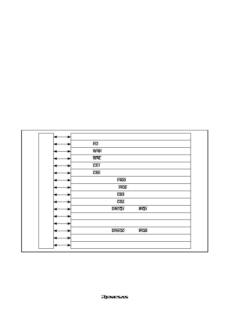
Rev. 2.0, 09/02, page 553 of 732
Section 18 I/O Ports
The SH7144 has six ports: A to F. Ports A, C, D, and E are 16-bit ports, and port B is a 10-bit port.
Port F is an 8-bit input-only port.
The SH7145 has six ports: A to F. Port A is a 24-bit port, port B is a 10-bit port, port C is a 16-bit
port, port D is a 32-bit port, and port E is a 16-bit port. Port F is an 8-bit input-only port.
All the port pins are multiplexed as general input/output pins and special function pins. The
functions of the multiplex pins are selected by means of the pin function controller (PFC). Each
port is provided with a data register for storing the pin data.
18.1
Port A
Port A in the SH7144 is an input/output port with the 16 pins shown in figure 18.1.
PA15 (I/O) / CK (output)
PA14 (I/O) /
(output)
PA13 (I/O) /
(output)
PA12 (I/O) /
(output)
PA11 (I/O) /
(output)
PA10 (I/O) /
(output)
PA9 (I/O) / TCLKD (input) /
(input)
PA8 (I/O) / TCLKC (input) /
(input)
PA7 (I/O) / TCLKB (input) /
(output)
PA6 (I/O) / TCLKA (input) /
(output)
PA5 (I/O) / SCK1 (I/O) /
(input) /
(input)
PA4 (I/O) / TXD1 (output)
PA3 (I/O) / RXD1 (input)
PA2 (I/O) / SCK0 (I/O) /
(input) /
(input)
PA1 (I/O) / TXD0 (output)
PA0 (I/O) / RXD0 (input)
Port A
Figure 18.1 Port A (SH7144)
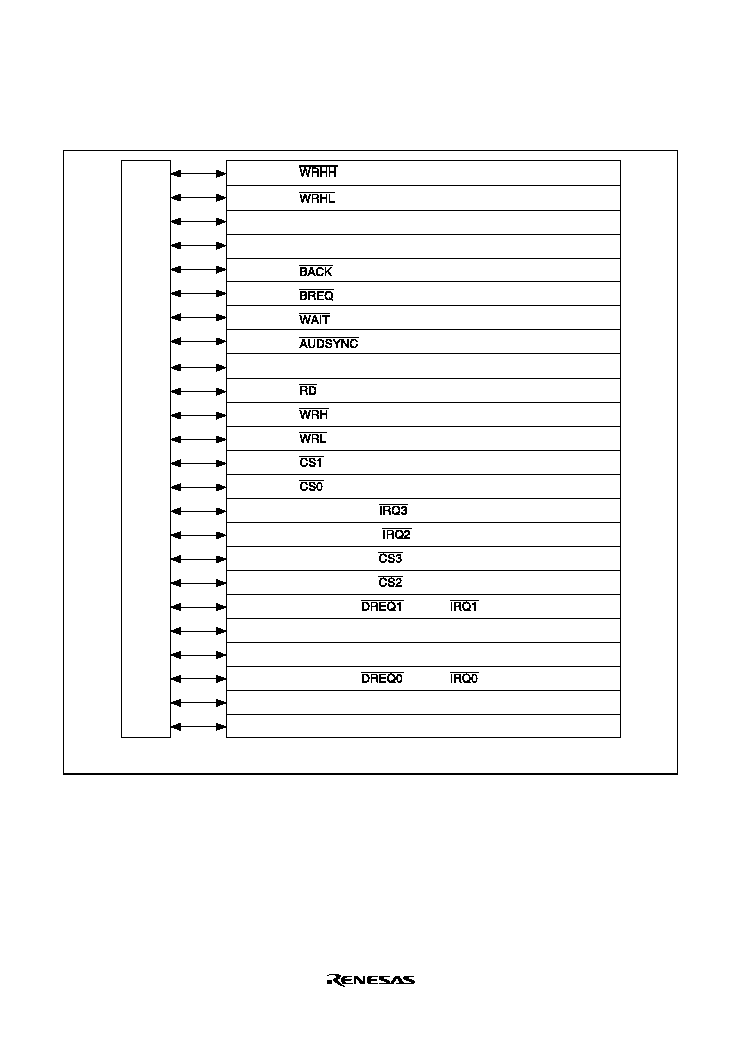
Rev. 2.0, 09/02, page 554 of 732
Port A in the SH7145 is an input/output port with the 24 pins shown in figure 18.2
PA15 (I/O) / CK (output)
PA14 (I/O) /
(output)
PA21 (I/O)
PA20 (I/O)
PA13 (I/O) /
(output)
PA23 (I/O) /
(output)
PA22 (I/O) /
(output)
PA12 (I/O) /
(output)
PA11 (I/O) /
(output)
PA10 (I/O) /
(output)
PA9 (I/O) / TCLKD (input) /
(input)
PA8 (I/O) / TCLKC (input) /
(input)
PA7 (I/O) / TCLKB (input) /
(output)
PA6 (I/O) / TCLKA (input) /
(output)
PA19 (I/O) /
(output) / DRAK1 (output)
PA18 (I/O) /
(input) / DRAK0 (output)
PA17 (I/O) /
(input)
PA16 (I/O) /
(I/O)
PA5 (I/O) / SCK1 (I/O) /
(input) /
(input)
PA4 (I/O) / TXD1 (output)
PA3 (I/O) / RXD1 (input)
PA2 (I/O) / SCK0 (I/O) /
(input) /
(input)
PA1 (I/O) / TXD0 (output)
PA0 (I/O) / RXD0 (input)
Port A
*
Note:
*
Only for the F-ZTAT version (no corresponding function in the mask version).
Figure 18.2 Port A (SH7145)

Rev. 2.0, 09/02, page 555 of 732
18.1.1
Register Descriptions
Port A is a 16-bit input/output port in the SH7144; a 24-bit input/output port in the SH7145. Port
A has the following registers. For details on register addresses and register states during each
processing, refer to section 25, List of Registers.
∑
Port A data register H (PADRH)
∑
Port A data register L (PADRL)
18.1.2
Port A Data Registers H and L (PADRH and PADRL)
The port A data registers H and L (PADRH and PADRL) are 16-bit readable/writable registers
that store port A data. Bits PA15DR to PA0DR correspond to pins PA15 to PA0 (multiplexed
functions omitted here) in the SH7144. Bits PA23DR to PA0DR correspond to pins PA23 to PA0
(multiplexed functions omitted here) in the SH7145.
When a pin functions is a general output, if a value is written to PADRH or PADRL, that value is
output directly from the pin, and if PADRH or PADRL is read, the register value is returned
directly regardless of the pin state.
When a pin functions is a general input, if PADRH or PADRL is read, the pin state, not the
register value, is returned directly. If a value is written to PADRH or PADRL, although that value
is written into PADRH or PADRL, it does not affect the pin state. Table 18.1 summarizes port A
data register L read/write operations.
PADRH:
Bit
Bit Name
Initial Value
R/W
Description
15 to
8
All 0
R
Reserved
These bits are always read as 0s and should always
be written with 0s.
7
PA23DR
0
R/W
See table 18.1
*
6
PA22DR
0
R/W
5
PA21DR
0
R/W
4
PA20DR
0
R/W
3
PA19DR
0
R/W
2
PA18DR
0
R/W
1
PA17DR
0
R/W
0
PA16DR
0
R/W
Note:
*
These bits are reserved in the SH7144. They are always read as 0s and should always
be written with 0s.

Rev. 2.0, 09/02, page 556 of 732
PADRL:
Bit
Bit Name
Initial Value
R/W
Description
15
PA15DR
0
R/W
See table 18.1
14
PA14DR
0
R/W
13
PA13DR
0
R/W
12
PA12DR
0
R/W
11
PA11DR
0
R/W
10
PA10DR
0
R/W
9
PA9DR
0
R/W
8
PA8DR
0
R/W
7
PA7DR
0
R/W
6
PA6DR
0
R/W
5
PA5DR
0
R/W
4
PA4DR
0
R/W
3
PA3DR
0
R/W
2
PA2DR
0
R/W
1
PA1DR
0
R/W
0
PA0DR
0
R/W
Table 18.1 Port A Data Register (PADR) Read/Write Operations
PADRH bits 7 to 0 and PADRL bits 15 to 0:
PAIORL, H
Pin Function
Read
Write
0
General input
Pin state
Can write to PADRH and PADRL, but it has no
effect on pin state
Other than
general input
Pin state
Can write to PADRH and PADRL, but it has no
effect on pin state
1
General output
PADRH or L
value
Value written is output from pin
Other than
general output
PADRH or L
value
Can write to PADRH and PADRL, but it has no
effect on pin state
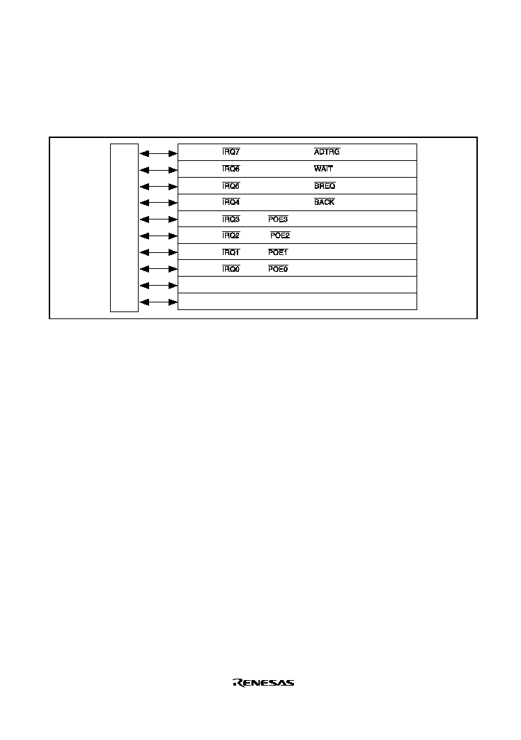
Rev. 2.0, 09/02, page 557 of 732
18.2
Port B
Port B is an input/output port with the 10 pins shown in figure 18.3.
PB3 (I/O) /
(input) /
(input) / SDA0 (I/O)
PB4 (I/O) /
(input) /
(input)
PB5 (I/O) /
(input) /
(input)
PB6 (I/O) /
(input) / A18 (output) /
(output)
PB7 (I/O) /
(input) / A19 (output) /
(input)
PB8 (I/O) /
(input) / A20 (output) /
(input)
PB9 (I/O) /
(input) / A21 (output) /
(input)
PB2 (I/O) /
(input) /
(input) / SCL0 (I/O)
PB1 (I/O) / A17 (output)
PB0 (I/O) / A16 (output)
Port B
Figure 18.3 Port B
18.2.1
Register Descriptions
Port B is a 10-bit input/output port. Port B has the following register. For details on register
addresses and register states during each processing, refer to section 25, List of Registers.
∑
Port B data register (PBDR)
18.2.2
Port B Data Register (PBDR)
The port B data register (PBDR) is a 16-bit readable/writable register that stores port B data. Bits
PB9DR to PB0DR correspond to pins PB9 to PB0 (multiplexed functions omitted here).
When a pin functions is a general output, if a value is written to PBDR, that value is output
directly from the pin, and if PBDR is read, the register value is returned directly regardless of the
pin state.
When a pin functions is a general input, if PBDR is read, the pin state, not the register value, is
returned directly. If a value is written to PBDR, although that value is written into PBDR, it does
not affect the pin state. Table 18.2 summarizes port B data register read/write operations.

Rev. 2.0, 09/02, page 558 of 732
Bit
Bit Name Initial Value
R/W
Description
15 to 10 --
All 0
R
Reserved
These bits are always read as 0s, and should only be
written with 0s.
9
PB9DR
0
R/W
See table 18.2
8
PB8DR
0
R/W
7
PB7DR
0
R/W
6
PB6DR
0
R/W
5
PB5DR
0
R/W
4
PB4DR
0
R/W
3
PB3DR
0
R/W
2
PB2DR
0
R/W
1
PB1DR
0
R/W
0
PB0DR
0
R/W
Table 18.2 Port B Data Register (PBDR) Read/Write Operations
Bits 9 to 0:
PBIOR
Pin Function
Read
Write
0
General input
Pin state
Can write to PBDR, but it has no effect on pin state
Other than
general input
Pin state
Can write to PBDR, but it has no effect on pin state
1
General output
PBDR value
Value written is output from pin
Other than
general output
PBDR value
Can write to PBDR, but it has no effect on pin state
Rev. 2.0, 09/02, page 559 of 732
18.3
Port C
Port C is an input/output port with 16 pins shown in figure 18.4.
PC15 (I/O) / A15 (output)
PC14 (I/O) / A14 (output)
PC13 (I/O) / A13 (output)
PC12 (I/O) / A12 (output)
PC11 (I/O) / A11 (output)
PC10 (I/O) / A10 (output)
PC9 (I/O) / A9 (output)
PC8 (I/O) / A8 (output)
PC7 (I/O) / A7 (output)
PC6 (I/O) / A6 (output)
PC5 (I/O) / A5 (output)
PC4 (I/O) / A4 (output)
PC3 (I/O) / A3 (output)
PC2 (I/O) / A2 (output)
PC1 (I/O) / A1 (output)
PC0 (I/O) / A0 (output)
Port C
Figure 18.4 Port C
18.3.1
Register Descriptions
Port C is a 16-bit input/output port. Port C has the following register. For details on register
addresses and register states during each processing, refer to section 25, List of Registers.
∑
Port C data register (PCDR)
18.3.2
Port C Data Register (PCDR)
The port C data register (PCDR) is a 16-bit readable/writable register that stores port C data. Bits
PC15DR to PC0DR correspond to pins PC15 to PC0 (multiplexed functions omitted here).
When a pin functions is a general output, if a value is written to PCDR, that value is output
directly from the pin, and if PCDR is read, the register value is returned directly regardless of the
pin state.

Rev. 2.0, 09/02, page 560 of 732
When a pin function is a general input, if PCDR is read, the pin state, not the register value, is
returned directly. If a value is written to PCDR, although that value is written into PCDR, it does
not affect the pin state. Table 18.3 summarizes port C data register read/write operations.
PCDR:
Bit
Bit Name
Initial Value
R/W
Description
15
PC15DR
0
R/W
See table 18.3
14
PC14DR
0
R/W
13
PC13DR
0
R/W
12
PC12DR
0
R/W
11
PC11DR
0
R/W
10
PC10DR
0
R/W
9
PC9DR
0
R/W
8
PC8DR
0
R/W
7
PC7DR
0
R/W
6
PC6DR
0
R/W
5
PC5DR
0
R/W
4
PC4DR
0
R/W
3
PC3DR
0
R/W
2
PC2DR
0
R/W
1
PC1DR
0
R/W
0
PC0DR
0
R/W
Table 18.3 Port C Data Register (PCDR) Read/Write Operations
Bits 15 to 0:
PCIOR
Pin Function
Read
Write
0
General input
Pin state
Can write to PCDR, but it has no effect on pin state
Other than
general input
Pin state
Can write to PCDR, but it has no effect on pin state
1
General output
PCDR value
Value written is output from pin
Other than
general output
PCDR value
Can write to PCDR, but it has no effect on pin state
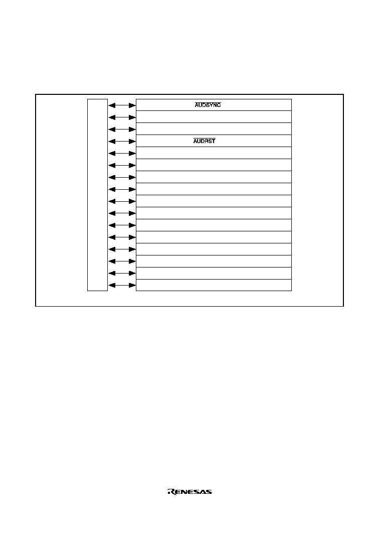
Rev. 2.0, 09/02, page 561 of 732
18.4
Port D
Port D of the SH7144 is an input/output port with 16 pins shown in figure 18.5.
PD15 (I/O) / D15 (I/O) /
(I/O)
*
PD14 (I/O) / D14 (I/O) / AUDCK (I/O)
*
PD13 (I/O) / D13 (I/O) / AUDMD (input)
*
PD12 (I/O) /D12 (I/O) /
(input)
*
PD11 (I/O) / D11 (I/O) / AUDATA3 (I/O)
*
PD10 (I/O) / D10 (I/O) / AUDATA2 (I/O)
*
PD9 (I/O) / D9 (I/O) / AUDATA1 (I/O)
*
PD8 (I/O) / D8 (I/O) / AUDATA0 (I/O)
*
PD7 (I/O) / D7 (I/O)
PD6 (I/O) / D6 (I/O)
PD5 (I/O) / D5 (I/O)
PD4 (I/O) / D4 (I/O)
PD3 (I/O) / D3 (I/O)
PD2 (I/O) / D2 (I/O)
PD1 (I/O) / D1 (I/O)
PD0 (I/O) / D0 (I/O)
Port D
Note:
*
Only for the F-ZTAT version (no corresponding function in the mask version).
Figure 18.5 Port D (SH7144)
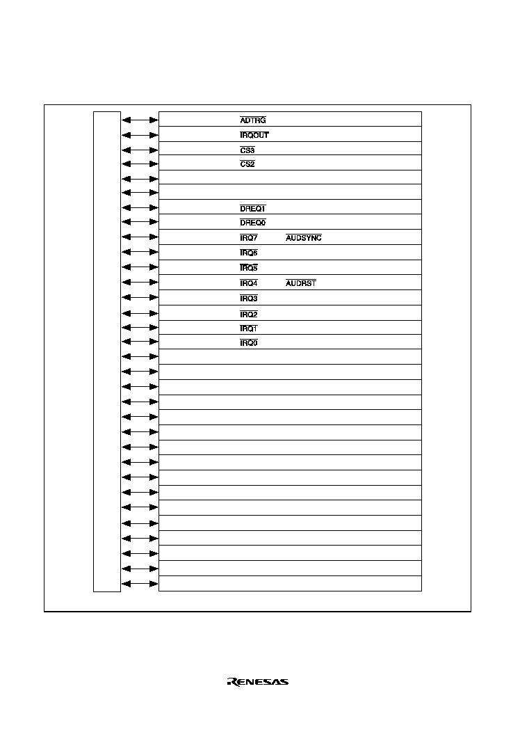
Rev. 2.0, 09/02, page 562 of 732
Port D of the SH7145 is an input/output port with 32 pins shown in figure 18.6.
PD25
(I/O) / D25 (I/O) /
(input)
PD24
(I/O) / D24 (I/O) /
(input)
PD23
(I/O) / D23 (I/O) /
(input) /
(I/O)
*
PD22
(I/O) / D22 (I/O) /
(input) / AUDCK (I/O)
*
PD21
(I/O) / D21 (I/O) /
(input) / AUDMD (input)
*
PD20
(I/O) / D20 (I/O) /
(input) /
(input)
*
PD19
(I/O) / D19 (I/O) /
(input) / AUDATA3 (I/O)
*
PD31
(I/O) / D31 (I/O) /
(input)
PD30
(I/O) / D30 (I/O) /
(output)
PD29
(I/O) / D29 (I/O) /
(output)
PD28
(I/O) / D28 (I/O) /
(output)
PD27
(I/O) / D27 (I/O) / DACK1 (output)
PD26
(I/O) / D26 (I/O) / DACK0 (output)
PD18
(I/O) / D18 (I/O) /
(input) / AUDATA2 (I/O)
*
PD17
(I/O) / D17 (I/O) /
(input) / AUDATA1 (I/O)
*
PD16
(I/O) / D16 (I/O) /
(input) / AUDATA0 (I/O)
*
PD15
(I/O) / D15 (I/O)
PD14
(I/O) / D14 (I/O)
PD13
(I/O) / D13 (I/O)
PD12
(I/O) / D12 (I/O)
PD11
(I/O) / D11 (I/O)
PD10
(I/O) / D10 (I/O)
PD9
(I/O) / D9 (I/O)
PD8
(I/O) / D8 (I/O)
PD7
(I/O) / D7 (I/O)
PD6
(I/O) / D6 (I/O)
PD5
(I/O) / D5 (I/O)
PD4
(I/O) / D4 (I/O)
PD3
(I/O) / D3 (I/O)
PD2
(I/O) / D2 (I/O)
PD1
(I/O) / D1 (I/O)
PD0
(I/O) / D0 (I/O)
Note:
*
Only for the F-ZTAT version (no corresponding function in the mask version).
Port D
Figure 18.6 Port D (SH7145)

Rev. 2.0, 09/02, page 563 of 732
18.4.1
Register Descriptions
Port D is a 16-bit input/output port in the SH7144; a 32-bit input/output port in the SH7145. Port
D has the following registers. For details on register addresses and register states during each
processing, refer to section 25, List of Registers.
∑
Port D data register H (PDDRH)
∑
Port D data register L (PDDRL)
18.4.2
Port D Data Registers H and L (PDDRH and PDDRL)
The port D data registers H and L (PDDRH and PDDRL) are 16-bit readable/writable registers
that store port D data. Bits PD15DR to PD0DR correspond to pins PD15 to PD0 (multiplexed
functions omitted here) in the SH7144. Bits PD31DR to PD0DR correspond to pins PD31 to PD0
(multiplexed functions omitted here) in the SH7145.
When a pin functions is a general output, if a value is written to PDDRH or PDDRL, that value is
output directly from the pin, and if PDDRH or PDDRL is read, the register value is returned
directly regardless of the pin state.
When a pin functions is a general input, if PDDRH or PDDRL is read, the pin state, not the
register value, is returned directly. If a value is written to PDDRH or PDDRL, although that value
is written into PDDRH or PDDRL, it does not affect the pin state. Table 18.4 summarizes port D
data register L read/write operations.

Rev. 2.0, 09/02, page 564 of 732
PDDRH:
Bit
Bit Name
Initial Value
R/W
Description
15
PD31DR
0
R/W
See table 18.4
*
14
PD30DR
0
R/W
13
PD29DR
0
R/W
12
PD28DR
0
R/W
11
PD27DR
0
R/W
10
PD26DR
0
R/W
9
PD25DR
0
R/W
8
PD24DR
0
R/W
7
PD23DR
0
R/W
6
PD22DR
0
R/W
5
PD21DR
0
R/W
4
PD20DR
0
R/W
3
PD19DR
0
R/W
2
PD18DR
0
R/W
1
PD17DR
0
R/W
0
PD16DR
0
R/W
Note:
*
These bits are reserved in the SH7144. They are always read as 0s and should always
be written with 0s.

Rev. 2.0, 09/02, page 565 of 732
PDDRL:
Bit
Bit Name
Initial Value
R/W
Description
15
PD15DR
0
R/W
See table 18.4
14
PD14DR
0
R/W
13
PD13DR
0
R/W
12
PD12DR
0
R/W
11
PD11DR
0
R/W
10
PD10DR
0
R/W
9
PD9DR
0
R/W
8
PD8DR
0
R/W
7
PD7DR
0
R/W
6
PD6DR
0
R/W
5
PD5DR
0
R/W
4
PD4DR
0
R/W
3
PD3DR
0
R/W
2
PD2DR
0
R/W
1
PD1DR
0
R/W
0
PD0DR
0
R/W
Table 18.4 Port D Data Register (PDDR) Read/Write Operations
PDDRH bits 15 to 0 and PDDRL bits 15 to 0:
PDIORL, H Pin Function
Read
Write
0
General input
Pin state
Can write to PDDRH or PDDRL, but it has no
effect on pin state
Other than
general input
Pin state
Can write to PDDRH or PDDRL, but it has no
effect on pin state
1
General output
PDDRH or L
value
Value written is output from pin
Other than
general output
PDDRH or L
value
Can write to PDDRH or PDDRL, but it has no
effect on pin state
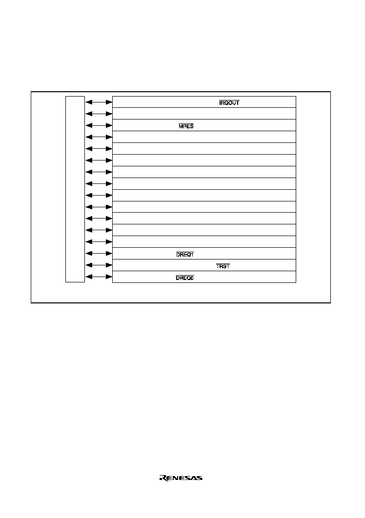
Rev. 2.0, 09/02, page 566 of 732
18.5
Port E
Port E in the SH7144 is an input/output port with the 16 pins shown in figure 18.7.
PE15 (I/O) / TIOC4D (I/O) / DACK1 (output) /
(output)
PE14 (I/O) / TIOC4C (I/O) / DACK0 (output)
PE13 (I/O) / TIOC4B (I/O) /
(input)
PE12 (I/O) / TIOC4A (I/O) / TXD3 (output)
PE11 (I/O) / TIOC3D (I/O) / RXD3 (input)
PE10 (I/O) / TIOC3C (I/O) / TXD2 (output)
PE9 (I/O) / TIOC3B (I/O) / SCK3 (I/O)
PE8 (I/O) / TIOC3A (I/O) / SCK2 (I/O)
PE7 (I/O) / TIOC2B (I/O) / RXD2 (input)
PE6 (I/O) / TIOC2A (I/O) / SCK3 (I/O)
PE5 (I/O) / TIOC1B (I/O) / TXD3 (output)
PE4 (I/O) / TIOC1A (I/O) / RXD3 (input) / TCK (input)
*
PE3 (I/O) / TIOC0D (I/O) / DRAK1 (output) / TDO (output)
*
PE2 (I/O) / TIOC0C (I/O) /
(input) / TDI (input)
*
PE1 (I/O) / TIOC0B (I/O) / DRAK0 (output) /
(input)
*
PE0 (I/O) / TIOC0A (I/O) /
(input) / TMS (input)
*
Port E
Note:
*
Only for the F-ZTAT version (no corresponding function in the mask version).
Figure 18.7 Port E (SH7144)
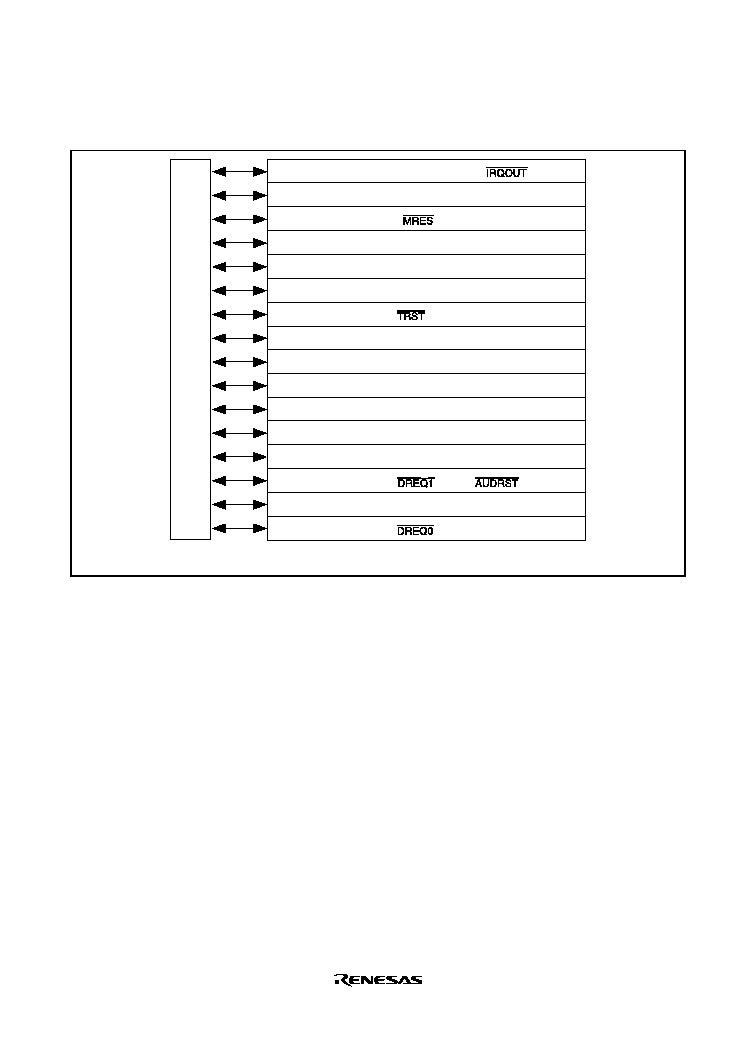
Rev. 2.0, 09/02, page 567 of 732
Port E in the SH7145 is an input/output port with the 16 pins shown in figure 18.8.
PE15 (I/O) / TIOC4D (I/O) / DACK1 (output) /
(output)
PE14 (I/O) / TIOC4C (I/O) / DACK0 (output)
PE13 (I/O) / TIOC4B (I/O) /
(input)
PE12 (I/O) / TIOC4A (I/O) / TCK (input)
*
/ TXD3 (output)
PE11 (I/O) / TIOC3D (I/O) / TDO (output)
*
/ RXD3 (input)
PE10 (I/O) / TIOC3C (I/O) / TXD2 (output) / TDI (input)
*
PE9 (I/O) / TIOC3B (I/O) /
(input)
*
/ SCK3 (I/O)
PE8 (I/O) / TIOC3A (I/O) / SCK2 (I/O) / TMS (input)
*
PE7 (I/O) / TIOC2B (I/O) / RXD2 (input)
PE6 (I/O) / TIOC2A (I/O) / SCK3 (I/O) / AUDATA0 (I/O)
*
PE5 (I/O) / TIOC1B (I/O) / TXD3 (output) / AUDATA1 (I/O)
*
PE4 (I/O) / TIOC1A (I/O) / RXD3 (input) / AUDATA2 (I/O)
*
PE3 (I/O) / TIOC0D (I/O) / DRAK1 (output) / AUDATA3 (I/O)
*
PE2 (I/O) / TIOC0C (I/O) /
(input) /
(input)
*
PE1 (I/O) / TIOC0B (I/O) / DRAK0 (output) / AUDMD (input)
*
PE0 (I/O) / TIOC0A (I/O) /
(input) / AUDCK (I/O)
*
Note:
*
Only for the F-ZTAT version (no corresponding function in the mask version).
Port E
Figure 18.8 Port E (SH7145)
18.5.1
Register Descriptions
Port E has the following register. For details on register addresses and register states during each
processing, refer to section 25, List of Registers.
∑
Port E data register L (PEDRL)
18.5.2
Port E Data Register L (PEDRL)
The port E data register L (PEDRL) is a 16-bit readable/writable registers that stores port E data.
Bits PE15DR to PE0DR correspond to pins PE15 to PE0 (multiplexed functions omitted here).
When a pin functions is a general output, if a value is written to PEDRL, that value is output
directly from the pin, and if PEDRL is read, the register value is returned directly regardless of the
pin state.

Rev. 2.0, 09/02, page 568 of 732
When a pin functions is a general input, if PEDRL is read, the pin state, not the register value, is
returned directly. If a value is written to PEDRL, although that value is written into PEDRL it
does not affect the pin state. Table 18.5 summarizes port E data register read/write operations.
PEDRL:
Bit
Bit Name
Initial Value
R/W
Description
15
PE15DR
0
R/W
See table 18.5
14
PE14DR
0
R/W
13
PE13DR
0
R/W
12
PE12DR
0
R/W
11
PE11DR
0
R/W
10
PE10DR
0
R/W
9
PE9DR
0
R/W
8
PE8DR
0
R/W
7
PE7DR
0
R/W
6
PE6DR
0
R/W
5
PE5DR
0
R/W
4
PE4DR
0
R/W
3
PE3DR
0
R/W
2
PE2DR
0
R/W
1
PE1DR
0
R/W
0
PE0DR
0
R/W
Table 18.5 Port E Data Register L (PEDRL) Read/Write Operations
Bits 15 to 0 in PEDRL:
PEIOR
Pin Function
Read
Write
0
General input
Pin state
Can write to PEDRL, but it has no effect on pin
state
Other than
general input
Pin state
Can write to PEDRL, but it has no effect on pin
state
1
General output
PEDRL value
Value written is output from pin
Other than
general output
PEDRL value
Can write to PEDRL, but it has no effect on pin
state
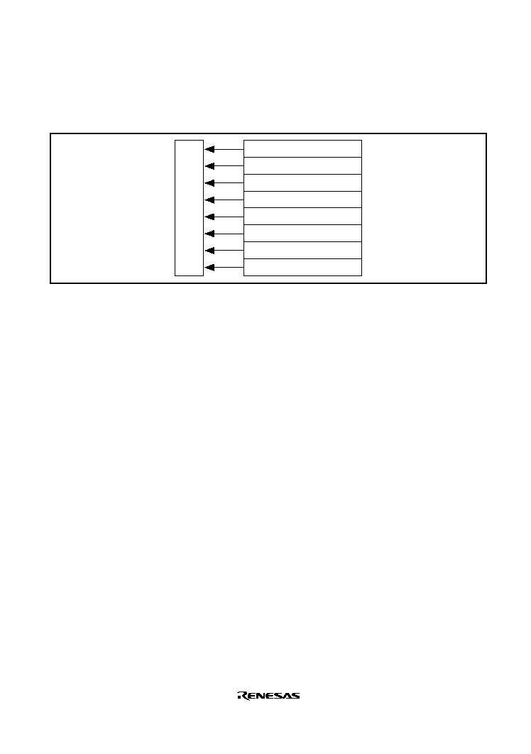
Rev. 2.0, 09/02, page 569 of 732
18.6
Port F
Port F is an input-only port with the eight pins shown in figure 18.9.
PF7 (input) / AN7 (input)
PF6 (input) / AN6 (input)
PF5 (input) / AN5 (input)
PF4 (input) / AN4 (input)
PF3 (input) / AN3 (input)
PF2 (input) / AN2 (input)
PF1 (input) / AN1 (input)
PF0 (input) / AN0 (input)
Port F
Figure 18.9 Port F
18.6.1
Register Descriptions
Port F is an 8-bit input-only port. Port F has the following register. For details on register
addresses and register states during each processing, refer to section 25, List of Registers.
∑
Port F data register (PFDR)
18.6.2
Port F Data Register (PFDR)
The port F data register (PFDR) is a 8-bit read-only register that stores port F data.
Bits PF7DR to PF0DR correspond to pins PF7 to PF0 (multiplexed functions omitted here).
Any value written into these bits is ignored, and there is no effect on the state of the pins. When
any of the bits are read, the pin state rather than the bit value is read directly. However, when an
A/D converter analog input is being sampled, values of 1 are read out. Table 18.6 summarizes port
F data register read/write operations.

Rev. 2.0, 09/02, page 570 of 732
Bit
Bit Name
Initial Value
R/W
Description
7
PF7DR
0/1
*
R
See table 18.6
*
6
PF6DR
0/1
*
R
5
PF5DR
0/1
*
R
4
PF4DR
0/1
*
R
3
PF3DR
0/1
*
R
2
PF2DR
0/1
*
R
1
PF1DR
0/1
*
R
0
PF0DR
0/1
*
R
Notes:
*
Initial values are dependent on the state of the pins.
Table 18.6 Port F Data Register (PFDR) Read/Write Operations
Bits 7 to 0:
Pin Function
Read
Write
General input
Pin state
Ignored (no effect on pin state)
ANn input (analog input)
1
Ignored (no effect on pin state)

ROM3251A_010020020700
Rev. 2.0, 09/02, page 571 of 732
Section 19 Flash Memory (F-ZTAT Version)
The features of the flash memory in the flash memory version are summarized below.
The block diagram of the flash memory is shown in figure 19.1.
19.1
Features
∑
Size: 256 kbytes
∑
Programming/erasing methods
The flash memory is programmed 128 bytes at a time. Erase is performed in single-block
units. The flash memory is configured as follows: 64 kbytes
◊
3 blocks, 32 kbytes
◊
1
block, and 4 kbytes
◊
8 blocks. To erase the entire flash memory, each block must be
erased in turn.
∑
Reprogramming capability
The flash memory can be reprogrammed up to 100 times.
∑
Two on-board programming modes
Boot mode
User program mode
On-board programming/erasing can be done in boot mode, in which the boot program built
into the chip is started to erase or program of the entire flash memory. In normal user
program mode, individual blocks can be erased or programmed.
∑
PROM programmer mode
Flash memory can be programmed/erased in programmer mode using a PROM
programmer, as well as in on-board programming mode.
∑
Automatic bit rate adjustment
With data transfer in boot mode, this LSI's bit rate can be automatically adjusted to match
the transfer bit rate of the host computer.
∑
Programming/erasing protection
Sets software protection against flash memory programming/erasing/verifying.
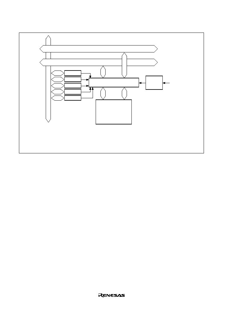
Rev. 2.0, 09/02, page 572 of 732
Module bus
Bus interface/controller
Flash memory
(256 kbytes)
Operating
mode
FLMCR2
Internal address bus
Internal data bus (32 bits)
FWP pin
Mode pin
EBR1
EBR2
RAMER
FLMCR1
Flash memory control register 1
Flash memory control register 2
Erase block register 1
Erase block register 2
RAM emulation register
Legend
FLMCR1:
FLMCR2:
EBR1:
EBR2:
RAMER:
Figure 19.1 Block Diagram of Flash Memory
19.2
Mode Transitions
When the mode pin and the FWP pin are set in the reset state and a reset-start is executed, this LSI
enters an operating mode as shown in figure 19.2. In user mode, flash memory can be read but not
programmed or erased.
The boot mode, user program mode, and PROM programmer modes are provided as modes to
write and erase the flash memory.
The differences between boot mode and user program mode are shown in table 19.1.
Figure 19.3 shows boot mode, and figure 19.4 shows user program mode.
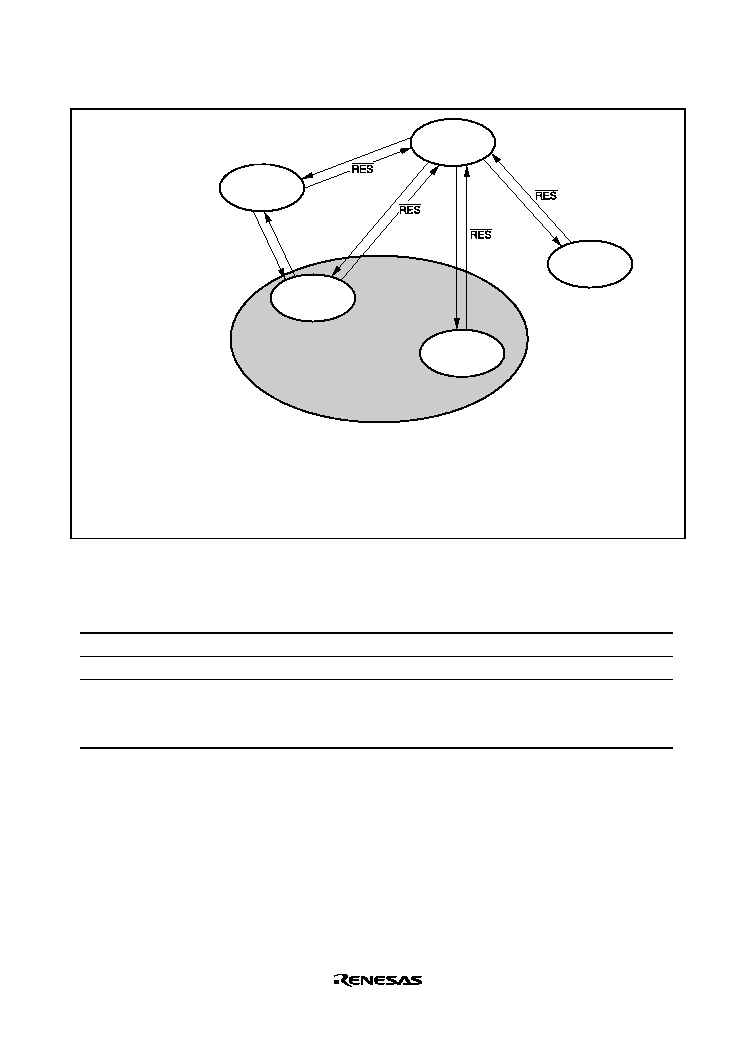
Rev. 2.0, 09/02, page 573 of 732
MD1 = 0,
FWP = 0
= 0
= 0
FWP = 0
FWP = 1
*
1
*
1
*
2
MD1 = 1,
FWP = 0
Reset state
Boot mode
On-board programming mode
User
program mode
User mode
(on-chip ROM
enabled)
MD1 = 1,
FWP = 1
PROM
programmer
mode
= 0
= 0
Notes: Only make a transition between user mode and user program mode when the CPU is not accessing
the flash memory.
1. RAM emulation possible
2. This LSI transits to PROM programmer mode by using the dedicated PROM programmer.
Figure 19.2 Flash Memory State Transitions
Table 19.1 Differences between Boot Mode and User Program Mode
Boot Mode
User Program Mode
Total erase
Yes
Yes
Block erase
No
Yes
Programming control program
*
Program/program-verify Erase/erase-verify
Program/program-verify
Emulation
Note:
*
To be provided by the user, in accordance with the recommended algorithm.
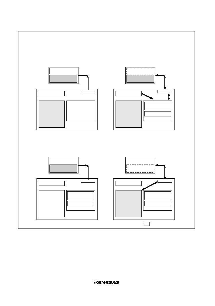
Rev. 2.0, 09/02, page 574 of 732
Flash memory
This LSI
RAM
Host
Programming control
program
SCI
Application program
(old version)
;;
New application
program
Flash memory
This LSI
RAM
Host
SCI
Application program
(old version)
Boot program area
New application
program
Flash memory
This LSI
RAM
Host
SCI
Flash memory
erase
Boot program
New application
program
Flash memory
This LSI
Program execution state
RAM
Host
SCI
New application
program
Boot program
Programming control
program
;;
;;;
;
;
;
1. Initial state
The old program version or data remains written
in the flash memory. The user should prepare the
programming control program and new
application program beforehand in the host.
2. Programming control program transfer
When boot mode is entered, the boot program in
this LSI (originally incorporated in the chip) is
started and the programming control program in
the host is transferred to RAM via SCI
communication. The boot program required for
flash memory erasing is automatically transferred
to the RAM boot program area.
3. Flash memory initialization
The erase program in the boot program area (in
RAM) is executed, and the flash memory is
initialized (to H'FF). In boot mode, total flash
memory erasure is performed, without regard to
blocks.
4. Writing new application program
The programming control program transferred
from the host to RAM is executed, and the new
application program in the host is written into the
flash memory.
Programming control
program
Boot program
Boot program
Boot program area
Boot program area
Programming control
program
Figure 19.3 Boot Mode
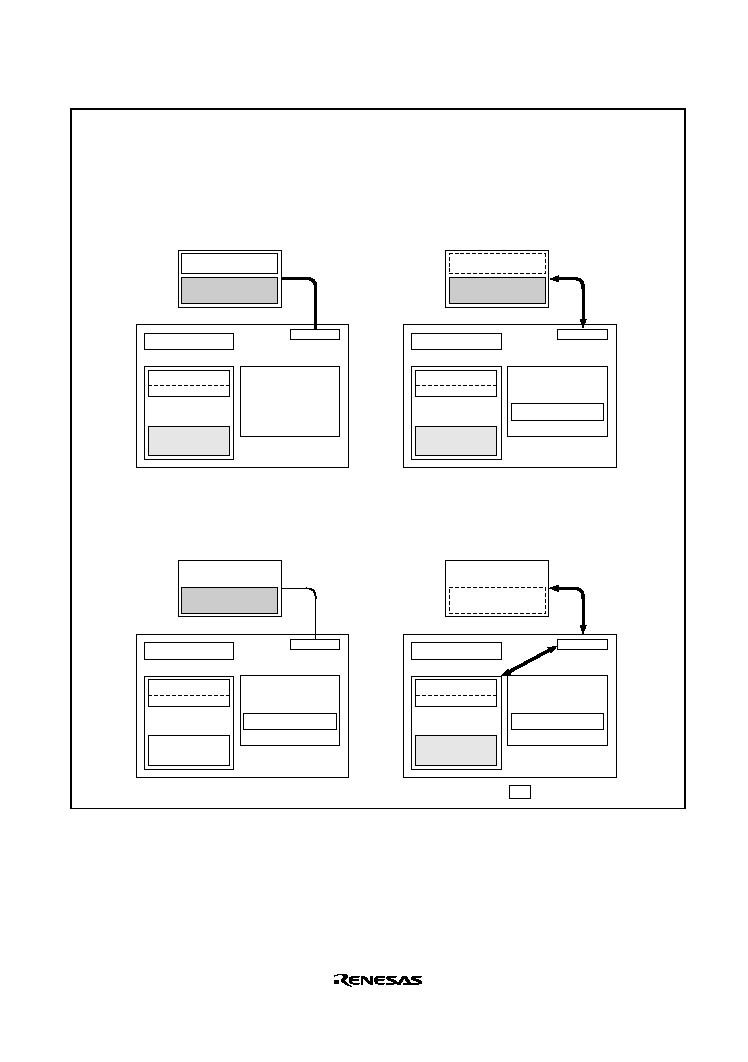
Rev. 2.0, 09/02, page 575 of 732
Flash memory
This LSI
RAM
Host
Programming/
erase control program
SCI
Boot program
New application
program
Flash memory
This LSI
RAM
Host
SCI
New application
program
Flash memory
This LSI
RAM
Host
SCI
Flash memory
erase
Boot program
New application
program
Flash memory
This LSI
Program execution state
RAM
Host
SCI
Boot program
;
;
Boot program
FWE assessment
program
Application program
(old version)
;
;;
New application
program
;;
1. Initial state
The FWE assessment program that confirms that
user program mode has been entered, and the
program that will transfer the programming/erase
control program from flash memory to on-chip
RAM should be written into the flash memory by
the user beforehand. The programming/erase
control program should be prepared in the host
or in the flash memory.
2. Programming/erase control program transfer
When user program mode is entered, user
software confirms this fact, executes transfer
program in the flash memory, and transfers the
programming/erase control program to RAM.
3. Flash memory initialization
The programming/erase program in RAM is
executed, and the flash memory is initialized (to
H'FF). Erasing can be performed in block units,
but not in byte units.
4. Writing new application program
Next, the new application program in the host is
written into the erased flash memory blocks. Do
not write to unerased blocks.
Programming/
erase control program
Programming/
erase control program
Programming/
erase control program
Transfer program
Application program
(old version)
Transfer program
FWE assessment
program
FWE assessment
program
Transfer program
FWE assessment
program
Transfer program
Figure 19.4 User Program Mode
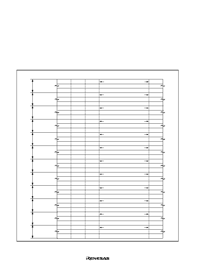
Rev. 2.0, 09/02, page 576 of 732
19.3
Block Configuration
Figure 19.5 shows the block configuration of 256-kbyte flash memory. The thick lines indicate
erasing units, the narrow lines indicate programming units, and the values are addresses. The flash
memory is divided into 64 kbytes (3 blocks), 32 kbytes (1 block), and 4 kbytes (8 blocks). Erasing
is performed in these units. Programming is performed in 128-byte units starting from an address
with lower eight bits H'00 or H'80.
EB0
EB1
EB2
EB3
EB4
EB5
EB6
EB7
EB8
EB9
H'000000
H'000FFF
H'00007F
H'004FFF
H'005FFF
H'001FFF
H'002FFF
H'003FFF
H'01FFFF
H'006FFF
H'007FFF
H'00FFFF
H'001000
H'002000
H'003000
H'004000
H'005000
H'006000
H'007000
H'008000
H'010000
EB10
H'02FFFF
H'020000
EB11
H'03FFFF
H'030000
Programming unit: 128 bytes
Programming unit: 128 bytes
Programming unit: 128 bytes
Programming unit: 128 bytes
Programming unit: 128 bytes
Programming unit: 128 bytes
Programming unit: 128 bytes
Programming unit: 128 bytes
Programming unit: 128 bytes
Programming unit: 128 bytes
Programming unit: 128 bytes
Programming unit: 128 bytes
Erase unit
4 kbytes
Erase unit
4 kbytes
Erase unit
4 kbytes
Erase unit
4 kbytes
Erase unit
4 kbytes
Erase unit
4 kbytes
Erase unit
4 kbytes
Erase unit
4 kbytes
Erase unit
32 kbytes
Erase unit
64 kbytes
Erase unit
64 kbytes
Erase unit
64 kbytes
-- -- -- -- -- -- -- -- -- --
-- -- -- -- -- -- -- -- -- --
-- -- -- -- -- -- -- -- -- --
-- -- -- -- -- -- -- -- -- --
-- -- -- -- -- -- -- -- -- --
-- -- -- -- -- -- -- -- -- --
-- -- -- -- -- -- -- -- -- --
-- -- -- -- -- -- -- -- -- --
-- -- -- -- -- -- -- -- -- --
-- -- -- -- -- -- -- -- -- --
-- -- -- -- -- -- -- -- -- --
-- -- -- -- -- -- -- -- -- --
Figure 19.5 Flash Memory Block Configuration

Rev. 2.0, 09/02, page 577 of 732
19.4
Input/Output Pins
The flash memory is controlled by means of the pins shown in table 19.2.
Table 19.2 Pin Configuration
Pin Name
I/O
Function
RES
Input
Reset
FWP
*
1
Input
Flash programming/erasing protection by hardware
MD1
Input
Sets this LSI's operating mode
MD0
Input
Sets this LSI's operating mode
TxD1 (PA4)
*
2
Output
Serial transmit data output
RxD1 (PA3)
*
2
Input
Serial receive data input
Notes: 1. Protection cannot be made to flash memory programming/erasing regardless of the
setting of the FWP pin when using E10A (when DBGMD is high)
2. In boot mode, SCI pins are fixed, and PA3 and PA4 pins are used as SCI pins.
19.5
Register Descriptions
The flash memory has the following registers. For details on register addresses and register states
during each processing, refer to section 25, List of Registers.
∑
Flash memory control register 1 (FLMCR1)
∑
Flash memory control register 2 (FLMCR2)
∑
Erase block register 1 (EBR1)
∑
Erase block register 2 (EBR2)
∑
RAM emulation register (RAMER)
19.5.1
Flash Memory Control Register 1 (FLMCR1)
FLMCR1 is a register that makes the flash memory change to program mode, program-verify
mode, erase mode, or erase-verify mode. For details on register setting, refer to section 19.8, Flash
Memory Programming/Erasing.

Rev. 2.0, 09/02, page 578 of 732
Bit
Bit Name
Initial Value
R/W
Description
7
FEW
1/0
R
Flash Write Enable
*
Reflects the input level at the FWP pin. It is set to 1
when a low level is input to the FWP pin, and cleared
to 0 when a high level is input.
6
SWE
0
R/W
Software Write Enable
When this bit is set to 1 while the FEW bit is 1, flash
memory programming/erasing is enabled. When this
bit is cleared to 0, other FLMCR1 bits and all EBR1
and EBR2 bits cannot be set.
5
ESU
0
R/W
Erase Setup
When this bit is set to 1 while the FEW and SWE bits
are 1, the flash memory changes to the erase setup
state. When it is cleared to 0, the erase setup state is
cancelled.
4
PSU
0
R/W
Program Setup
When this bit is set to 1 while the FEW and SWE bits
are 1, the flash memory changes to the program
setup state. When it is cleared to 0, the program
setup state is cancelled.
3
EV
0
R/W
Erase-Verify
When this bit is set to 1 while the FEW and SWE bits
are 1, the flash memory changes to erase-verify
mode. When it is cleared to 0, erase-verify mode is
cancelled.
2
PV
0
R/W
Program-Verify
When this bit is set to 1 while the FEW and SWE bits
are 1, the flash memory changes to program-verify
mode. When it is cleared to 0, program-verify mode is
cancelled.
1
E
0
R/W
Erase
When this bit is set to 1 while the FEW, SWE and
ESU bits are 1, the flash memory changes to erase
mode. When it is cleared to 0, erase mode is
cancelled.
0
P
0
R/W
Program
When this bit is set to 1 while the FEW, SWE and
PSU bits are 1, the flash memory changes to program
mode. When it is cleared to 0, program mode is
cancelled.
Note:
*
The value of this bit is 1 when using E10A (when DBGMD is high).

Rev. 2.0, 09/02, page 579 of 732
19.5.2
Flash Memory Control Register 2 (FLMCR2)
FLMCR2 is a register that displays the state of flash memory programming/erasing.
Bit
Bit Name
Initial Value
R/W
Description
7
FLER
0
R
Indicates that an error has occurred during an
operation on flash memory (programming or erasing).
When FLER is set to 1, flash memory goes to the
error-protection state.
See section 19.9.3, Error Protection, for details.
6 to 0 --
All 0
R
Reserved
These bits are always read as 0.
19.5.3
Erase Block Register 1 (EBR1)
EBR1 specifies the flash memory erase block. EBR1 is initialized to H'00 when a high level is
input to the FWP pin. It is also initialized to H'00, when the SWE bit in FLMCR1 is 0 regardless
of value in the FWP pin. Do not set more than one bit at a time in EBR1 and EBR2, as this will
cause all the bits in EBR1 and EBR2 to be automatically cleared to 0.
Bit
Bit Name
Initial Value
R/W
Description
7
EB7
0
R/W
When this bit is set to 1, 4 kbytes of EB7 (H'007000
to H'007FFF) are to be erased.
6
EB6
0
R/W
When this bit is set to 1, 4 kbytes of EB6 (H'006000
to H'006FFF) are to be erased.
5
EB5
0
R/W
When this bit is set to 1, 4 kbytes of EB5 (H'005000
to H'005FFF) are to be erased.
4
EB4
0
R/W
When this bit is set to 1, 4 kbytes of EB4 (H'004000
to H'004FFF) are to be erased.
3
EB3
0
R/W
When this bit is set to 1, 4 kbytes of EB3 (H'003000
to H'003FFF) are to be erased.
2
EB2
0
R/W
When this bit is set to 1, 4 kbytes of EB2 (H'002000
to H'002FFF) are to be erased.
1
EB1
0
R/W
When this bit is set to 1, 4 kbytes of EB1 (H'001000
to H'001FFF) are to be erased.
0
EB0
0
R/W
When this bit is set to 1, 4 kbytes of EB0 (H'000000
to H'000FFF) are to be erased.

Rev. 2.0, 09/02, page 580 of 732
19.5.4
Erase Block Register 2 (EBR2)
EBR2 specifies the flash memory erase block. EBR2 is initialized to H'00 when a high level is
input to the FWP pin. It is also initialized to H'00, when the SWE bit in FLMCR1 is 0 regardless
of value in the FWP pin. Do not set more than one bit at a time in EBR1 and EBR2, as this will
cause all the bits in EBR1 and EBR2 to be automatically cleared to 0.
Bit
Bit Name Initial Value
R/W
Description
7 to 4
--
All 0
R
Reserved
These bits are always read as 0 and should only be
written with 0
3
EB11
0
R/W
When this bit is set to 1, 64 kbytes of EB11
(H'030000 to H'03FFFF) are to be erased.
2
EB10
0
R/W
When this bit is set to 1, 64 kbytes of EB10
(H'020000 to H'02FFFF) are to be erased.
1
EB9
0
R/W
When this bit is set to 1, 64 kbytes of EB9 (H'010000
to H'01FFFF) will be erased.
0
EB8
0
R/W
When this bit is set to 1, 32 kbytes of EB8 (H'008000
to H'00FFFF) will be erased.
19.5.5
RAM Emulation Register (RAMER)
RAMER specifies the area of flash memory to be overlapped with part of RAM when emulating
real-time flash memory programming. RAMER settings should be made in user mode or user
program mode. To ensure correct operation of the emulation function, the ROM for which RAM
emulation is performed should not be accessed immediately after this register has been modified.
Normal execution of an access immediately after register modification is not guaranteed.
Bit
Bit Name Initial Value
R/W
Description
15 to 4
--
All 0
R
Reserved
These bits are always read as 0 and should only be
written with 0
3
RAMS
0
R/W
RAM Select
Specifies selection or non-selection of flash memory
emulation in RAM. When RAMS = 1, the flash
memory is overlapped with part of RAM, and all flash
memory blocks are program/erase-protected. When
RAMS = 0, the RAM emulation function is disabled.

Rev. 2.0, 09/02, page 581 of 732
Bit
Bit Name Initial Value
R/W
Description
2
1
0
RAM2
RAM1
RAM0
0
0
0
R/W
R/W
R/W
Flash Memory Area Selection
When the RAMS bit is set to 1, these bits specify one
of the following flash memory areas to be overlapped
with part of RAM.
000: H'00000000 to H'00000FFF (EB0)
001: H'00001000 to H'00001FFF (EB1)
010: H'00002000 to H'00002FFF (EB2)
011: H'00003000 to H'00003FFF (EB3)
100: H'00004000 to H'00004FFF (EB4)
101: H'00005000 to H'00005FFF (EB5)
110: H'00006000 to H'00006FFF (EB6)
111: H'00007000 to H'00007FFF (EB7)
19.6
On-Board Programming Modes
There are two modes for programming/erasing of the flash memory; boot mode, which enables on-
board programming/erasing, and PROM programmer mode, in which programming/erasing is
performed with a PROM programmer. On-board programming/erasing can also be performed in
user program mode. At reset-start in reset mode, this LSI changes to a mode depending on the MD
pin settings and FWP pin setting, as shown in table 19.3.
When changing to boot mode, the boot program built into this LSI is initiated. The boot program
transfers the programming control program from the externally-connected host to on-chip RAM
via SCI1. After erasing the entire flash memory, the programming control program is executed.
This can be used for programming initial values in the on-board state or for a forcible return when
programming/erasing can no longer be done in user program mode. In user program mode,
individual blocks can be erased and programmed by branching to the user program/erase control
program prepared by the user.
Table 19.3 Setting On-Board Programming Modes
MD1
MD0
FWP
LSI State after Reset End
0
Expanded mode
0
1
Boot mode
Single-chip mode
0
Expanded mode
1
1
0
User program mode
Single-chip mode

Rev. 2.0, 09/02, page 582 of 732
19.6.1
Boot Mode
Table 19.4 shows the boot mode operations between reset end and branching to the programming
control program.
1. When boot mode is used, the flash memory programming control program must be prepared in
the host beforehand. Prepare a programming control program in accordance with the
description in section 19.8, Flash Memory Programming/Erasing.
2. The SCI1 should be set to asynchronous mode, and the transfer format as follows: 8-bit data, 1
stop bit, and no parity.
3. When the boot program is initiated, the chip measures the low-level period of asynchronous
SCI communication data (H'00) transmitted continuously from the host. The chip then
calculates the bit rate of transmission from the host, and adjusts the SCI1 bit rate to match that
of the host. The reset should end with the RxD pin high. The RxD and TxD pins should be
pulled up on the board if necessary.
4. After matching the bit rates, the chip transmits one H'00 byte to the host to indicate the
completion of bit rate adjustment. The host should confirm that this adjustment end indication
(H'00) has been received normally, and transmit one H'55 byte to the chip. If reception could
not be performed normally, initiate boot mode again by a reset. Depending on the host's
transfer bit rate and system clock frequency of this LSI, there will be a discrepancy between
the bit rates of the host and the chip. To operate the SCI properly, set the host's transfer bit rate
and system clock frequency of this LSI within the ranges listed in table 19.5.
5. In boot mode, a part of the on-chip RAM area is used by the boot program. The area
H'FFFFE800 to H'FFFFFFFF is the area to which the programming control program is
transferred from the host. The boot program area cannot be used until the execution state in
boot mode switches to the programming control program.
6. Before branching to the programming control program, the chip terminates transfer operations
by SCI1 (by clearing the RE and TE bits in SCR to 0), however the adjusted bit rate value
remains set in BRR. Therefore, the programming control program can still use it for transfer of
write data or verify data with the host. The TxD pin is high. The contents of the CPU general
registers are undefined immediately after branching to the programming control program.
These registers must be initialized at the beginning of the programming control program, as the
stack pointer (SP), in particular, is used implicitly in subroutine calls, etc.
7. Boot mode can be cleared by a reset. End the reset after driving the reset pin low, waiting at
least 20 states, and then setting the mode (MD) pins. Boot mode is also cleared when a WDT
overflow occurs.
8.
Do not change the MD pin input levels in boot mode.
9.
All interrupts are disabled during programming or erasing of the flash memory.
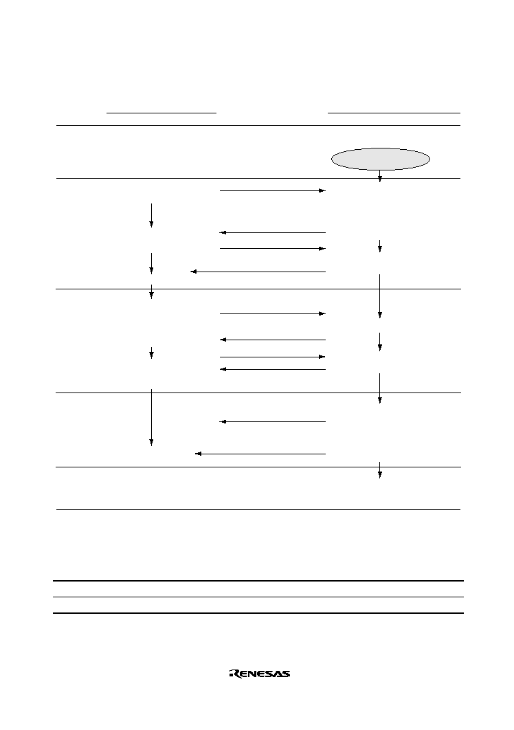
Rev. 2.0, 09/02, page 583 of 732
Table 19.4 Boot Mode Operation
Item
Host Operation
Communications Contents
LSI Operation
Boot mode
start
Branches to boot program at
reset-start.
Processing Contents
Processing Contents
Bit rate
adjustment
Continuously transmits data
H'00 at specified bit rate.
H'00, H'00 ...... H'00
H'00
H'55
∑ Measures low-level period of receive
data H'00.
∑ Calculates bit rate and sets it in BRR
of SCI_1.
∑ Transmits data H'00 to host as
adjustment end indication.
Transmits data H'AA to host when
data H'55 is received.
Transmits data H'55 when
data H'00 is received
error-free.
Transmits number of bytes (N)
of programming control as
program to be transferred
2-byte data (lower byte
following upper byte)
Receives data H'AA.
Transmits 1-byte of
programming control program
(repeated for N times)
Receives data H'AA.
Transfer of
programming
control
program
Flash
memory
erase
Boot program initiation
Echobacks the 2-byte data received.
Branches to programming control
program transferred to on-chip RAM
and starts execution.
Echobacks received data to host and
also transfers it to RAM (repeated
for N times)
Checks flash memory data, erases all
flash memory blocks in case of written
data existing, and transmits data H'AA
to host. (If erase could not be done,
transmits data H'FF to host and
aborts operation.)
Upper byte and
lower byte
H'XX
H'AA
Echoback
Echoback
H'FF
H'AA
Boot program
erase error
Table 19.5 Peripheral Clock (P
) Frequencies for which Automatic Adjustment of LSI Bit
Rate is Possible
Host Bit Rate
Peripheral Clock Frequency Range of LSI
9,600 bps
4 to 40 MHz
19,200 bps
8 to 40 MHz
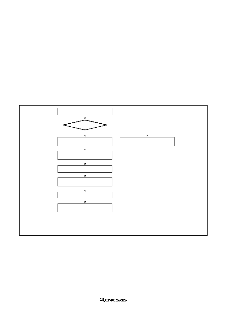
Rev. 2.0, 09/02, page 584 of 732
19.6.2
Programming/Erasing in User Program Mode
On-board programming/erasing of an individual flash memory block can also be performed in user
program mode by branching to a user program/erase control program. The user must set branching
conditions and provide on-board means of supplying programming data. The flash memory must
contain the user program/erase control program or a program that provides the user program/erase
control program from external memory. As the flash memory itself cannot be read during
programming/erasing, transfer the user program/erase control program to on-chip RAM or
external memory, and execute it. Figure 19.6 shows a sample procedure for programming/erasing
in user program mode. Prepare a user program/erase control program in accordance with the
description in section 19.8, Flash Memory Programming/Erasing.
Yes
No
Program/erase?
Transfer user program/erase
control program to RAM
Reset-start
Branch to user program/erase
control program in RAM
Execute user program/erase control
program (flash memory rewrite)
Branch to flash memory
application program
Branch to flash memory
application program
FWP = low
*
FWP = high
Note:
*
Do not constantly apply a low level to the FWP pin. Only apply a low level to the FWP pin when
programming or erasing the flash memory. To prevent excessive programming or excessive erasing,
while a low level is being applied to the FWP pin, activate the watchdog timer in case of handling CPU
runaways.
Figure 19.6 Programming/Erasing Flowchart Example in User Program Mode
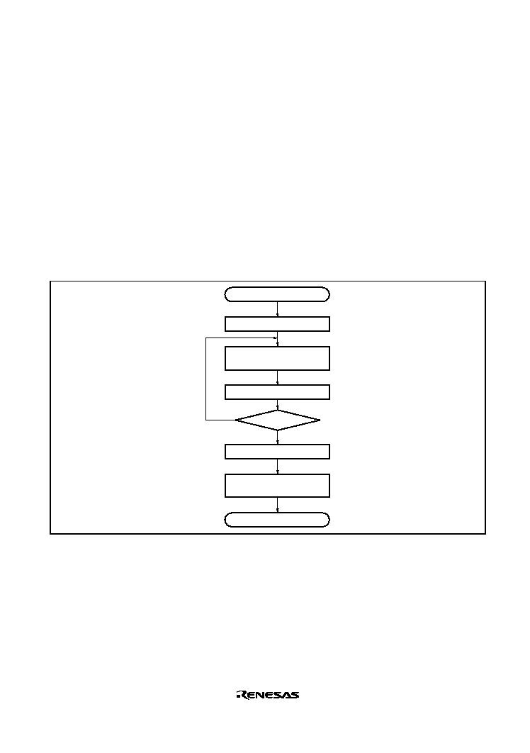
Rev. 2.0, 09/02, page 585 of 732
19.7
Flash Memory Emulation in RAM
A setting in the RAM emulation register (RAMER) enables part of RAM to overlap with the flash
memory area so that data to be written to flash memory can be emulated in RAM in real time.
Emulation can be performed in user mode or user program mode. Figure 19.7 shows an example
of emulation of real-time flash memory programming.
1. Set RAMER to overlap part of RAM with the area for which real-time programming is
required.
2. Emulation is performed using the overlapped RAM.
3. After the program data has been confirmed, the RAMS bit is cleared, thus releasing the RAM
overlap.
4. The data written in the overlapped RAM is written into the flash memory area.
Set RAMER
Write tuning data to
overlapped RAM
Execute application program
Tuning OK?
Clear RAMER
Write to flash memory
emulation block
No
Yes
Start of emulation program
End of emulation program
Figure 19.7 Flowchart for Flash Memory Emulation in RAM
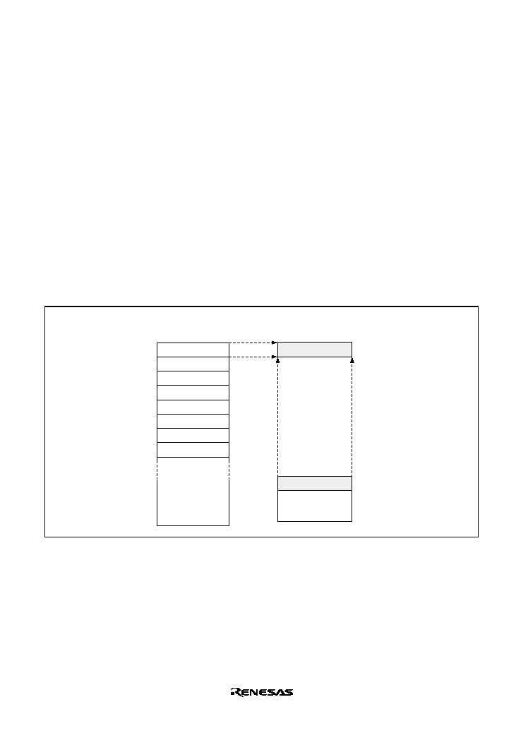
Rev. 2.0, 09/02, page 586 of 732
Figure 19.8 shows a sample procedure for flash memory block area overlapping.
1. The RAM area to be overlapped is fixed at a 4-kbyte area in the range H'FFFFE000 to
H'FFFFEFFF.
2. The flash memory area to be overlapped is selected by RAMER from a 4-kbyte area of the
EB0 to EB7 blocks.
3. The overlapped RAM area can be accessed from both the flash memory addresses and RAM
addresses.
4. When the RAMS bit in RAMER is set to 1, program/erase protection is enabled for all flash
memory blocks (emulation protection). In this state, setting the P or E bit in FLMCR1 to 1
does not cause a transition to program mode or erase mode.
5. A RAM area cannot be erased by execution of software in accordance with the erase
algorithm.
6. Block area EB0 contains the vector table. When performing RAM emulation, the vector table
is needed in the overlapped RAM.
EB0
H'00000
H'01000
H'02000
H'03000
H'04000
H'05000
H'06000
H'07000
H'08000
H'3FFFF
EB1
EB2
EB3
EB4
EB5
EB6
EB7
EB8 to EB11
H'FFFFE000
H'FFFFEFFF
H'FFFFFFFF
This area can be accessed from
both the flash memory addresses
and RAM addressed.
Flash Memory
On-chip RAM
Figure 19.8 Example of RAM Overlap Operation (RAM[2:0]
=
=
=
=
B'000)

Rev. 2.0, 09/02, page 587 of 732
19.8
Flash Memory Programming/Erasing
A software method using the CPU is employed to program and erase the flash memory in on-
board programming modes. Depending on the FLMCR1 and FLMCR2 settings, the flash memory
operates in one of the following four modes: Program mode, program-verify mode, erase mode,
and erase-verify mode. The programming control program in boot mode and the user
program/erase control program in user program mode use these operating modes in combination to
perform programming/erasing. Flash memory programming and erasing should be performed in
accordance with the descriptions in section 19.8.1, Program/Program-Verify and section 19.8.2,
Erase/Erase-Verify, respectively.
19.8.1
Program/Program-Verify Mode
When writing data or programs to the flash memory, the program/program-verify flowchart shown
in figure 19.9 should be followed. Performing programming operations according to this flowchart
will enable data or programs to be written to the flash memory without subjecting the chip to
voltage stress or sacrificing program data reliability.
1. Programming must be done to an empty address. Do not reprogram an address to which
programming has already been performed.
2. Programming should be carried out 128 bytes at a time. A 128-byte data transfer must be
performed even if writing fewer than 128 bytes. In this case, H'FF data must be written to the
extra addresses.
3. Prepare the following data storage areas in RAM: A 128-byte programming data area, a 128-
byte reprogramming data area, and a 128-byte additional-programming data area. Perform
reprogramming data computation and additional programming data computation according to
figure 19.9.
4. Consecutively transfer 128 bytes of data in byte units from the reprogramming data area or
additional-programming data area to the flash memory. The program address and 128-byte
data are latched in the flash memory. The lower 8 bits of the start address in the flash memory
destination area must be H'00 or H'80.
5. The time during which the P bit is set to 1 is the programming time. Figure 19.9 shows the
allowable programming time.
6. The watchdog timer (WDT) is set to prevent overprogramming due to program runaway, etc.
An overflow cycle of approximately 6.6 ms is allowed.
7.
For a dummy write to a verify address, write 1-byte data H'FF to an address to be read. Verify
data can be read in longwords from the address to which a dummy write was performed.
8.
The number of repetitions of the program/program-verify sequence to the same bit should not
exceed the maximum number of programming (N).
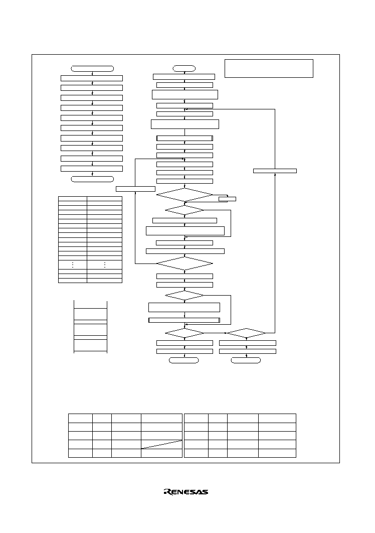
Rev. 2.0, 09/02, page 588 of 732
START
End Sub
1
2
3
4
5
6
7
8
9
10
11
12
13
998
999
1000
t
sp
30
t
sp
30
t
sp
30
t
sp
30
t
sp
30
t
sp
30
t
sp
200
t
sp
200
t
sp
200
t
sp
200
t
sp
200
t
sp
200
t
sp
200
t
sp
200
t
sp
200
t
sp
200
NG
NG
NG
NG
OK
OK
OK
*
2
*
7
*
7
*
4
*
7
*
7
*
5
*
7
*
7
*
1
*
4
*
3
*
7
*
7
*
7
*
1
*
4
OK
NG
OK
NG
OK
RAM
End of programming
Set SWE bit in FLMCR1
Start of programming
Wait (t
sswe
)
µ
s
n = 1
m = 0
Wait (t
spv
)
µ
s
Wait (t
spvr
)
µ
s
Wait (t
cpv
)
µ
s
Apply
Write Pulse (tsp30 or tsp200)
Sub-Routine-Call
Set PV bit in FLMCR1
H'FF dummy write to verify address
Read verify data
Write data =
verify data?
Transfer reprogram data to reprogram data area
Reprogram data computation
Transfer additional-programming data to
additional-programming data area
Additional-programming data computation
Clear PV bit in FLMCR1
Clear SWE bit in FLMCR1
m = 1
Reprogram
See note *6 for pulse width
m = 0 ?
Increment address
Programming failure
Clear SWE bit in FLMCR1
Wait (t
cswe
)
µ
s
6
n?
6
n ?
Wait (t
cswe
)
µ
s
n
N?
n
n + 1
Store 128-byte program data in program
data area and reprogram data area
Apply Write Pulse (tsp10) (Additional programming)
128-byte
data verification completed?
Successively write 128-byte data from additional-
programming data area in RAM to flash memory
Perform programming in the erased state.
Do not perform additional programming
on previously programmed addresses.
Original Data
(D)
Verify Data
(V)
Reprogram Data
(X)
Comments
Programming completed
Still in erased state; no action
Programming incomplete;
reprogram
Reprogram Data Computation Table
Reprogram Data
(X')
Verify Data
(V)
Additional-
Programming Data (Y)
1
1
1
1
0
1
0
0
0
0
1
1
Comments
Additional programming
to be executed
Additional programming
not to be executed
Additional programming
not to be executed
Additional programming
not to be executed
0
1
1
1
0
1
0
1
0
0
1
1
Additional-Programming Data Computation Table
Notes: 1. Data transfer is performed by byte transfer. The lower 8 bits of the start address to be written to must be H'00 or H'80.
A 128-byte data transfer must be performed even if writing fewer than 128 bytes; in this case, H'FF data must be written to the extra addresses.
2. Verify data is read in 32-bit (longword) units.
3. Reprogram data is determined by the operation shown in the table below (comparison between the data stored in the program data area and the verify data). Bits for
which the reprogram data is 0 are programmed in the next reprogramming loop. Therefore, even bits for which programming has been completed will be subjected to
programming once again if the subsequent verify operation ends in failure.
4. A 128-byte area for the storage of programming data, a 128-byte area for the storage of reprogramming data, and a 128-byte area for the storage of additional-
programming data must be provided in RAM. The contents of the reprogram data area and additional-program data area are modified as programming proceeds.
5. A write pulse of 30
µ
s or 200
µ
s is applied according to the progress of the programming operation. See note 6 for details of the pulse widths. When writing of
additional-programming data is executed, a 10
µ
s write pulse should be applied. Reprogram data X' means reprogram data when the write pulse is applied.
7. The wait times and value of N are shown in section 26.5, Flash Memory Characteristics.
Program data storage
area (128 bytes)
Reprogram data storage
area (128 bytes)
Additional-programming
data storage area
(128 bytes)
Number of Writes n
Note: 6. Write Pulse Width
Write Time (tsp)
µ
s
*
Use a
t
sp
10 write pulse for additional programming.
Write pulse application subroutine
Apply Write Pulse
Set PSU bit in FLMCR1
Enable WDT
Disable WDT
Wait (t
spsu
)
µ
s
Set P bit in FLMCR1
Wait (tsp10, tsp30, or tsp200)
µ
s
Clear P bit in FLMCR1
Wait (t
cp
)
µ
s
Clear PSU bit in FLMCR1
Wait (t
cpsu
)
µ
s
Start of programming
End of programming
*
7
Successively write 128-byte data from reprogram
data area in RAM to flash memory
Figure 19.9 Program/Program-Verify Flowchart

Rev. 2.0, 09/02, page 589 of 732
19.8.2
Erase/Erase-Verify Mode
When erasing flash memory, the erase/erase-verify flowchart shown in figure 19.10 should be
followed.
1. Prewriting (setting erase block data to all 0s) is not necessary.
2. Erasing is performed in block units. Make only a single-bit specification in the erase block
register 1 (EBR1) and the erase block register 2 (EBR2). To erase multiple blocks, each block
must be erased in turn.
3. The time during which the E bit is set to 1 is the flash memory erase time.
4. The watchdog timer (WDT) is set to prevent overerasing due to program runaway, etc. An
overflow cycle of approximately 19.8 ms is allowed.
5. For a dummy write to a verify address, write 1-byte data H'FF to the read address. Verify data
can be read in longwords from the address to which a dummy write was performed.
6. If the read data is not erased successfully, set erase mode again, and repeat the erase/erase-
verify sequence as before. The number of repetitions of the erase/erase-verify sequence should
not exceed the maximum number of erasing (N).
19.8.3
Interrupt Handling when Programming/Erasing Flash Memory
All interrupts, including the NMI interrupt, are disabled while flash memory is being programmed
or erased, or while the boot program is executing, for the following three reasons:
1. An interrupt during programming/erasing may cause a violation of the programming or erasing
algorithm, with the result that normal operation cannot be assured.
2. If an interrupt exception handling starts before the vector address is written or during
programming/erasing, a correct vector cannot be fetched and the CPU malfunctions.
3. If an interrupt occurs during boot program execution, normal boot mode sequence cannot be
carried out.
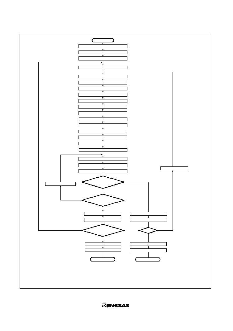
Rev. 2.0, 09/02, page 590 of 732
No
No
Yes
Yes
Yes
No
No
Yes
*
1
*
3
*
2
*
4
Erase start
Set EBR1 and EBR2
Enable WDT
Disable WDT
Read verify data
Increment address
Verify data = all 1s?
Last address of block?
All erase block erased?
Set block start address as verify address
H'FF dummy write to verify address
SWE bit
1
n
1
ESU bit
1
E bit
1
Wait (t
SSWE
)
µ
s
Wait (t
SESU
)
E bit
0
EV bit
1
Wait (t
SE
)
ESU bit
0
Wait (t
CE
)
Wait (t
CESU
)
Wait (t
SEV
)
EV bit
0
n
n + 1
Wait (t
CEV
)
SWE bit
0
Wait (t
CSWE
)
EV bit
0
n
100?
Wait (t
CEV
)
SWE bit
0
Wait (t
CSWE
)
Erase failure
End of erasing
Wait (t
SEVR
)
Notes: 1. Prewriting (setting erase block data to all 0s) is not necessary.
2. Verify data is read in 32-bit (longword) units.
3. Make only a single-bit specification in the erase block register 1 (EBR1) and the erase block
register 2 (EBR2).
4. Erasing is performed in block units. To erase multiple blocks, each block must be erased in turn.
Figure 19.10 Erase/Erase-Verify Flowchart

Rev. 2.0, 09/02, page 591 of 732
19.9
Program/Erase Protection
There are three kinds of flash memory program/erase protection; hardware protection, software
protection, and error protection.
19.9.1
Hardware Protection
Hardware protection refers to a state in which programming/erasing of flash memory is forcibly
disabled or aborted. Flash memory control register 1 (FLMCR1), flash memory control register 2
(FLMCR2), erase block register 1 (EBR1), and erase block register 2 (EBR2) are initialized
Protect Function
Item
Description
Program
Erase
FWP pin protect
When a high level is input to the FWP pin,
FLMCR1, EBR 1, and EBR 2 are initialized, and the
program/erase protection state is entered.
*
Yes
Yes
Reset/standby
protect
In the reset state (including the reset state when
the WDT overflows) and standby mode, FLMCR1,
EBR 1, and EBR 2 are initialized, and the
program/erase protection state is entered.
In a reset via the
RES
pin, the reset state is not
entered unless the
RES
pin is held low until
oscillation stabilizes after powering on. In the case
of a reset during operation, hold the
RES
pin low
for the
RES
pulse width specified in the AC
Characteristics section.
Yes
Yes
Note:
*
Protection by the FWP pin cannot be made when using E10A (when DBGMD is high).

Rev. 2.0, 09/02, page 592 of 732
19.9.2
Software Protection
Software protection can be implemented against programming/erasing of all flash memory blocks
by clearing the SWE bit in FLMCR1. When software protection is in effect, setting the P or E bit
in FLMCR1 does not cause a transition to program mode or erase mode. By setting the erase block
register 1 (EBR1), erase protection can be set for individual blocks. When EBR1 is set to H'00,
erase protection is set for all blocks.
Protect Function
Item
Description
Program
Erase
SWE bit protect
When the SWE bit in FLMCR1 is cleared to 0,
all blocks are program/erase-protected. (This
setting should be carried out in on-chip RAM or
external memory.)
Yes
Yes
Block protect
By setting the erase block register 1 (EBR1) and
the erase block register 2 (EBR2), erase
protection can be set for individual blocks.
When both EBR1 and EBR2 are set to H'00,
erase protection is set for all blocks.
--
Yes
Emulation protect
When the RAMS bit in RAMER is set to 1, all
blocks are program/erase-protected.
Yes
Yes
19.9.3
Error Protection
In error protection, an error is detected when CPU runaway occurs during flash memory
programming/erasing, or operation is not performed in accordance with the program/erase
algorithm, and the program/erase operation is forcibly aborted. Aborting the program/erase
operation prevents damage to the flash memory due to overprogramming or overerasing.
When the following errors are detected during programming/erasing of flash memory, the FLER
bit in FLMCR2 is set to 1, and the error protection state is entered.
∑
When the flash memory is read during programming/erasing (including vector read and
instruction fetch)
∑
Immediately after exception handling (excluding a reset) during programming/erasing
∑
When a SLEEP instruction is executed during programming/erasing
The FLMCR1, FLMCR2, EBR1, and EBR2 settings are retained, however program mode or erase
mode is forcibly aborted at the point when the error is detected. Program mode or erase mode
cannot be re-entered by re-setting the P1 or E1 bit. However, PV and EV bit settings are retained,
and a transition can be made to verify mode. The error protection state can be cancelled by the
power-on reset only.

Rev. 2.0, 09/02, page 593 of 732
19.10
PROM Programmer Mode
In PROM programmer mode, a PROM programmer can be used to perform programming/erasing
via a socket adapter, just as for a discrete flash memory. Use a PROM programmer that supports
the Hitachi 256-kbyte flash memory on-chip MCU device type (FZTAT256V3A).
19.11
Usage Note
∑
Module Standby Mode Setting
Access to flash memory can be enabled/disabled by the module standby control register
(MSTCR1). The initial value enables access to flash memory. Flash memory access is disabled
by setting the module standby control register. For details, see section 24, Power-Down
Modes.
19.12
Notes when Converting the F-ZTAT Versions to the Mask-ROM
Versions
Please note the following when converting the F-ZTAT versions to the mask-ROM versions, with
using the F-ZTAT application software.
In the mask-ROM version, addresses of the flash memory registers (refer to section 25.1, Register
Addresses Table (In the Order from Lower Addresses)) return undefined value if read.
When the F-ZTAT application software is used in the mask-ROM version, the FWP pin level
cannot be determined. When converting the program, make sure the reprogramming
(erasing/programming) part of the flash memory and the RAM emulation part not to be initiated.
In the mask-ROM version, boot mode pin setting should not be performed.
Note:
This difference applies to all the F-ZTAT versions and all the mask-ROM versions that
have different ROM size.

Rev. 2.0, 09/02, page 594 of 732
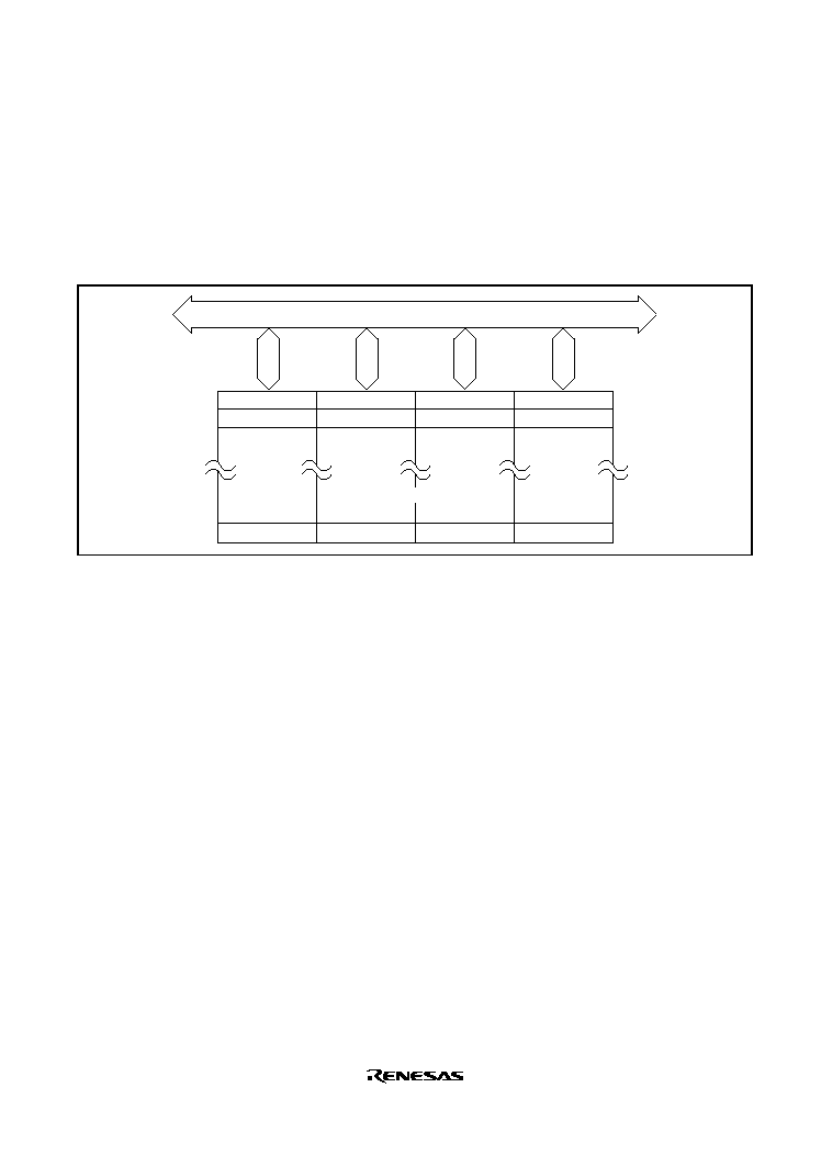
Rev. 2.0, 09/02, page 595 of 732
Section 20 Mask ROM
This LSI is available with 256 kbytes of on-chip mask ROM. The on-chip ROM is connected to
the CPU, direct memory access controller (DMAC), and data transfer controller (DTC) through a
32-bit data bus (figure 20.1). The CPU, DMAC, and DTC can access the on-chip ROM in 8, 16
and 32-bit widths. Data in the on-chip ROM can always be accessed in one cycle.
H'00000000
H'00000004
H'00000001
H'00000005
H'00000002
H'00000006
H'00000003
H'00000007
H'0003FFFC
H'0003FFFD
H'0003FFFE
H'0003FFFF
Internal data bus (32 bits)
On-chip ROM
Figure 20.1 Mask ROM Block Diagram
The operating mode, determines whether the on-chip ROM is valid or not. The operating mode is
selected using mode-setting pins FWP and MD3-MD0 as shown in table 3.1. If you are using the
on-chip ROM, select mode 2 or mode 3; if you are not, select mode 0 or 1. The on-chip ROM is
allocated to addresses H'00000000 to H'0003FFFF of memory area 0.
20.1
Usage Note
∑
Module Standby Mode Setting
Access to the on-chip ROM can be enabled/disabled by the module standby control register
(MSTCR1). The initial value enables the on-chip ROM operation. On-chip ROM access is
disabled by setting the module standby mode. For details, see section 24, Power-Down Modes.

Rev. 2.0, 09/02, page 596 of 732

RAM0200A_000020010800
Rev. 2.0, 09/02, page 597 of 732
Section 21 RAM
This LSI has an on-chip high-speed static RAM. The on-chip RAM is connected to the CPU,
direct memory access controller (DMAC), data transfer controller (DTC), and advanced user
debugger (AUD)* by a 32-bit data bus, enabling 8, 16, or 32-bit width access to data in the on-
chip RAM. Data in the on-chip RAM can always be accessed in one cycle, providing high-speed
access that makes this RAM ideal for use as a program area, stack area, or data area. The on-chip
RAM is allocated to address H
FFFFE000 to H
FFFFFFFF. The contents of the on-chip RAM are
retained in both sleep and standby modes.
The on-chip RAM can be enabled or disabled by means of the RAME bit in the system control
register (SYSCR). For details on the system control register (SYSCR), refer to section 24.2.2,
System Control Register (SYSCR).
Note: * Flash version only.
21.1
Usage Note
∑
Module Standby Mode Setting
RAM can be enabled/disabled by the module standby control register (MSTCR1). The initial
value enables RAM operation. RAM access is disabled by setting the module standby mode.
For details, see section 24, Power-Down Modes.

Rev. 2.0, 09/02, page 598 of 732

HUD0001A_010020020700
Rev. 2.0, 09/02, page 599 of 732
Section 22 Hitachi User Debug Interface (H-UDI)
22.1
Overview
The Hitachi user debug interface (H-UDI) provides data transfer and interrupt request functions.
The H-UDI performs serial transfer by means of external signal control.
22.1.1
Features
The H-UDI has the following features:
∑
Five test signals (TCK, TDI, TDO, TMS, and
TRST)
∑
TAP controller
∑
Two instructions
Bypass mode
Test mode conforming to IEEE 1149.1
H-UDI interrupt
H-UDI interrupt request to INTC
Note:
This LSI does not support test modes other than the bypass mode.
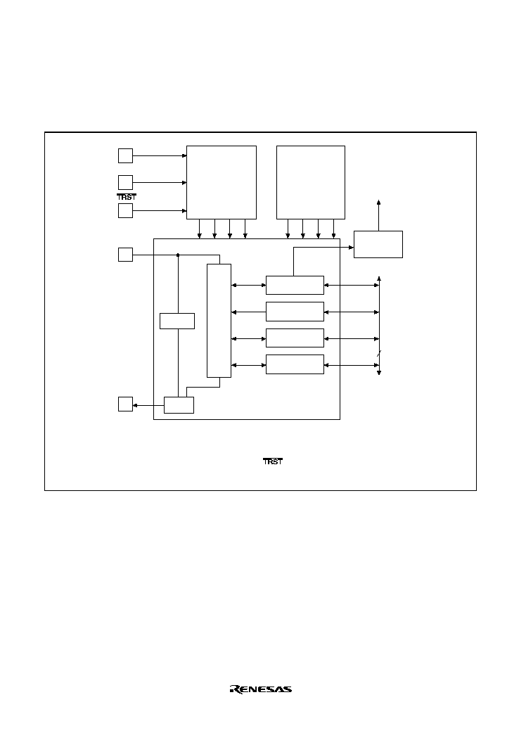
Rev. 2.0, 09/02, page 600 of 732
22.1.2
Block Diagram
Figure 22.1 shows a block diagram of the H-UDI.
TAP
controller
TCK
TMS
TDI
TDO
H-UDI
interrupt
signal
SDIR:
SDSR:
SDDRH:
SDDRL:
SDBPR:
Legend:
Mux
Decoder
Internal
bus
controller
Instruction register
Status register
Data register H
Data register L
Bypass register
TCK:
TMS:
:
TDI:
TDO:
Test clock
Test mode select
Test reset
Test data input
Test data output
Peripheral bus
SDBPR
Shift register
SDIR
SDSR
SDDRH
SDDRL
16
Figure 22.1 H-UDI Block Diagram

Rev. 2.0, 09/02, page 601 of 732
22.2
Input/Output Pins
Table 22.1 shows the H-UDI pin configuration.
Table 22.1 H-UDI Pins
Pin Name
Abbreviation
I/O
Function
Test clock
TCK
Input
Test clock input
TCK supplies an independent clock to the H-UDI. As
the clock input to TCK is supplied directly to the H-UDI,
a clock waveform with a duty cycle close to 50%
should be input (see section 26, Electrical
Characteristics, for details).
Test mode
select
TMS
Input
Test mode select input signal
TMS is sampled at the rising edge of TCK. TMS
controls the internal state of the TAP controller.
Test data
input
TDI
Input
Serial data input
TDI performs serial input of instructions and data to H-
UDI registers. TDI is sampled at the rising edge of
TCK.
Test data
output
TDO
Output
Serial data output
TDO performs serial output of instructions and data
from H-UDI registers. Transfer is synchronized with
TCK. When no signal is being output, TDO goes to the
high-impedance state.
Test reset
TRST
Input
Test reset input signal
TRST
is used to initialize the H-UDI asynchronously.
22.3
Register Description
The H-UDI has the following registers. For the register addresses and register states in each
operating mode, refer to section 25, List of Registers.
∑
Instruction register (SDIR)
∑
Status register (SDSR)
∑
Data register H (SDDRH)
∑
Data register L (SDDRL)
∑
Bypass register (SDBPR)
Instructions and data can be input to the instruction register (SDIR) and data register (SDDR) by
serial transfer from the test data input pin (TDI). Data from the status register (SDSR), and SDDR
can be output via the test data output pin (TDO). The bypass register (SDBPR) is a one-bit register

Rev. 2.0, 09/02, page 602 of 732
that is connected to TDI and TDO in bypass mode. Except for SDBPR, all the registers can be
accessed by the CPU.
Table 22.2 shows the kinds of serial transfer that can be used with each of the H-UDI's registers.
Table 22.2 Serial Transfer Characteristics of H-UDI Registers
Register
Serial Input
Serial Output
SDIR
Possible
Not possible
SDSR
Not possible
Possible
SDDRH
Possible
Possible
SDDRL
Possible
Possible
SDBPR
Possible
Possible
22.3.1
Instruction Register (SDIR)
The instruction register (SDIR) is a 16-bit register that can be read, but not written to, by the CPU.
H-UDI instructions can be transferred to SDIR from TDI by serial input. SDIR can be initialized
by the
TRST signal, but is not initialized in software standby mode.
Instructions transferred to SDIR must be 4 bits in length. If an instruction exceeding 4 bits is input,
the last 4 bits of the serial data will be stored in SDIR.
Bit
Bit
Name
Initial
value
R/W
Description
15
14
13
12
TS3
TS2
TS1
TS0
1
1
1
1
R
R
R
R
Test set bit
0xxx: setting prohibited
100x: setting prohibited
1010: H-UDI interrupt
1011: setting prohibited
110x: setting prohibited
1110: setting prohibited
1111: BYPASS mode
11 to 0
All 0
R
Reserved
These bits are always read as 0, and should only be
written with 0.

Rev. 2.0, 09/02, page 603 of 732
22.3.2
Status Register (SDSR)
The status register (SDSR) is a 16-bit register that can be read and written to by the CPU. The
SDSR value can be output from TDO, but serial data cannot be written to SDSR via TDI. The
SDTRF bit is output by means of a one-bit shift. In a two-bit shift, the SDTRF bit is output first,
followed by a reserved bit.
SDSR is initialized by
TRST signal input, but is not initialized in software standby mode.
Bit
Bit
Name
Initial
value
R/W
Description
15 to 12
All 0
R
These bits are always read as 0, and should only be
written with 0.
11
1
R
This bit is always read as 1, and should only be written
with 1.
10 to 1
All 0
R
This bit is always read as 0, and should only be written
with 0.
0
SDTRF
1
R/W
Serial Data Transfer Control Flag
Indicates whether H-UDI registers can be accessed by
the CPU. The SDTRF bit is initialized by the
TRST
signal, but is not initialized in software standby mode.
0: Serial transfer to SDDR has ended, and SDDR can be
accessed
1: Serial transfer to SDDR is in progress

Rev. 2.0, 09/02, page 604 of 732
22.3.3
Data Register (SDDR)
The data register (SDDR) comprises data register H (SDDRH) and data register L (SDDRL).
SDDRH and SDDRL are 16-bit registers that can be read and written to by the CPU. SDDR is
connected to TDO and TDI for serial data transfer to and from an external device.
32-bit data is input and output in serial data transfer. If data exceeding 32 bits is input, only the
last 32 bits will be stored in SDDR. Serial data is input starting with the MSB of SDDR (bit 15 of
SDDRH), and output starting with the LSB (bit 0 of SDDRL).
SDDR is not initialized by a reset, in software standby mode, or by the
TRST signal.
The initial value of SDDR is undefined.
22.3.4
Bypass Register (SDBPR)
The bypass register (SDBPR) is a one-bit shift register. In bypass mode, SDBPR is connected to
TDI and TDO, and this LSI is bypassed in a board test. SDBPR cannot be read or written to by the
CPU.

Rev. 2.0, 09/02, page 605 of 732
22.4
Operation
22.4.1
H-UDI Interrupt
When an H-UDI interrupt instruction is transferred to SDIR via TDI, an interrupt is generated.
Data transfer can be controlled by means of the H-UDI interrupt service routine. Transfer can be
performed by means of SDDR.
Control of data input/output between an external device and the H-UDI is performed by
monitoring the SDTRF bit in SDSR externally and internally. Internal SDTRF bit monitoring is
carried out by having SDSR read by the CPU.
The H-UDI interrupt and serial transfer procedure is as follows.
1. An instruction is input to SDIR by serial transfer, and an H-UDI interrupt request is generated.
2. After the H-UDI interrupt request is issued, the SDTRF bit in SDSR is monitored externally.
After output of SDTRF = 1 from TDO is observed, serial data is transferred to SDDR.
3. On completion of the serial transfer to SDDR, the SDTRF bit is cleared to 0, and SDDR can be
accessed by the CPU. After SDDR has been accessed, SDDR serial transfer is enabled by
setting the SDTRF bit in SDSR to 1.
4. Serial data transfer between an external device and the H-UDI can be carried out by constantly
monitoring the SDTRF bit in SDSR externally and internally.
Figures 22.2, 22.3, and 22.4 show the timing of data transfer between an external device and the
H-UDI.
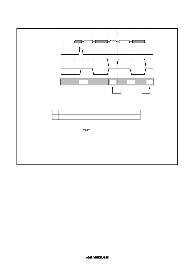
Rev. 2.0, 09/02, page 606 of 732
SDTRF
(in SDSR)
*
1
H-UDI interrupt
request
Serial data
SDSR and SDDR
MUX
*
2
SDDR access
state
Input/
output
SDTRF
Input
Shift
enabled
SDDR
SDDR
SDSR
SDSR serial transfer
(monitoring)
Instruc-
tion
1
1
0
Shift
disabled
SDSR
Shift
Shift
CPU
CPU
Notes: 1. SDTRF flag (in SDSR): Indicates whether SDDR access by the CPU or serial transfer
data input/output to SDDR is possible.
1
SDDR is shift-enabled. Do not access SDDR until SDTRF = 0.
0
SDDR is shift-disabled. SDDR access by the CPU is enabled.
Conditions: ∑ SDTRF = 1
-- When
= 0
-- When the CPU writes 1
-- In bypass mode
∑ SDTRF = 0
-- End of SDDR shift access in serial transfer
2. SDSR/SDDR (Update-DR state) internal MUX switchover timing
∑ Switchover from SDSR to SDDR: On completion of serial transfer in which
SDTRF = 1 is output from TDO
∑ Switchover from SDDR to SDSR: On completion of serial transfer to SDDR
Shift
enabled
Figure 22.2 Data Input/Output Timing Chart (1)
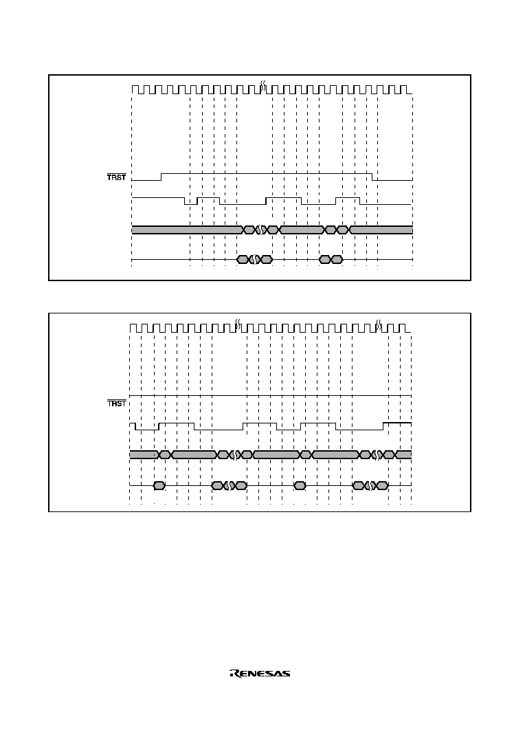
Rev. 2.0, 09/02, page 607 of 732
TCK
TMS
TDI
TDO
Test-Logic-Reset
Run-Test/Idle
Select-DR
Select-IR
Capture-IR
Shift-IR
Update-IR
Select-DR
Capture-DR
Shift-DR
Test-Logic-Reset
Run-Test/Idle
Exit1-DR
Update-DR
TS0
TS3
SDTRF
Exit1-IR
Figure 22.3 Data Input/Output Timing Chart (2)
TCK
TMS
TDI
TDO
Select-DR
Select-DR
Capture-DR
Shift-DR
Exit1-DR
Update-DR
Select-DR
Capture-DR
Shift-DR
Update-DR
Bit
0
SDTRF
Shift-DR
Capture-DR
Shift-DR
Select-DR
Update-DR
Capture-DR
Update-DR
Exit1-DR
Exit1-DR
Exit1-DR
Bit
31
Bit
0
Bit
31
SDTRF
Bit
0
Bit
31
Bit
0
Bit
31
Figure 22.4 Data Input/Output Timing Chart (3)

Rev. 2.0, 09/02, page 608 of 732
22.4.2
Bypass Mode
Bypass mode can be used to bypass this LSI in a boundary-scan test. Bypass mode is entered by
transferring B'1111 to SDIR. In bypass mode, SDBPR is connected to TDI and TDO.
22.4.3
H-UDI Reset
The H-UDI can be reset as follows.
∑
By holding the
TRST signal at 0
∑
When
TRST = 1, by inputting at least five TCK clock cycles while TMS = 1
22.5
Usage Notes
∑
The registers are not initialized in software standby mode. If
TRST is set to 0 in software
standby mode, bypass mode will be entered.
∑
The frequency of TCK must be lower than that of the peripheral module clock (P
). For
details, see section 26, Electrical Characteristics.
∑
In serial data transfer, data input/output starts with the LSB. Figure 22.5 shows serial data
input/output.
∑
If the H-UDI serial transfer sequence is disrupted, a
TRST reset must be executed. Transfer
should then be retried, regardless of the transfer operation.
∑
The TDO output timing is from the rise of TCK.
∑
In the Shift-IR state, the lower 2 bits of the output data from TDO (the IR status word) may not
always be 01.
∑
If more than 32 bits are serially transferred, serial data exceeding 32 bits output from TDO
should be ignored.
∑
The TDI pin must not be in the high-impedance state.
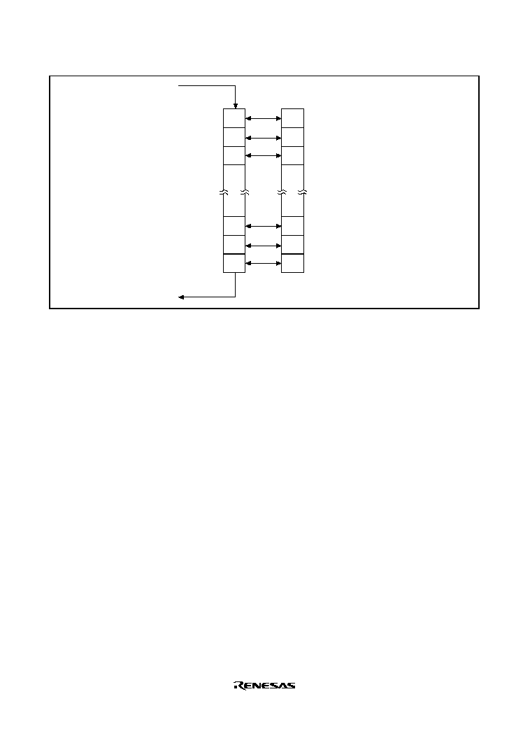
Rev. 2.0, 09/02, page 609 of 732
Shift register
SDIR, SDSR,
SDDRH/SDDRL
31
30
1
0
TDI
TDO
Serial data
input/output is in
LSB-first order.
Figure 22.5 Serial Data Input/Output

Rev. 2.0, 09/02, page 610 of 732

AUD0001A_010020020700
Rev. 2.0, 09/02, page 611 of 732
Section 23 Advanced User Debugger (AUD)
23.1
Overview
This LSI has an on-chip advanced user debugger (AUD). Use of the AUD simplifies the
construction of a simple emulator, with functions such as acquisition of branch trace data and
monitoring/tuning of on-chip RAM data.
AUD can be enabled or disabled using the AUDSRST bit in the system control register (SYSCR).
Refer to section 24.2.2, System Control Register (SYSCR), for SYSCR.
23.1.1
Features
The AUD has the following features:
∑
Eight input/output pins
Data bus (AUDATA3-AUDATA0)
AUD reset (
AUDRST)
AUD sync signal (
AUDSYNC)
AUD clock (AUDCK)
AUD mode (AUDMD)
∑
Two modes
Branch trace mode
RAM monitor mode
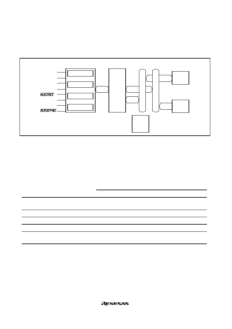
Rev. 2.0, 09/02, page 612 of 732
23.1.2
Block Diagram
Figure 23.1 shows a block diagram of the AUD.
PC output circuit
Address buffer
Data buffer
Mode control
Internal
bus
Bus
controller
Peripheral
module bus
On-chip
memory
On-chip
peripheral
module
CPU
AUDATA0
AUDATA1
AUDATA2
AUDATA3
AUDMD
AUDCK
Figure 23.1 AUD Block Diagram
23.2
Input/Output Pins
Table 23.1 shows the AUD's input/output pins.
Table 23.1 AUD Pin Configuration
Function
Name
Abbreviation
Branch Trace Mode
RAM Monitor Mode
AUD data
AUDATA3 to
AUDATA0
Branch destination address
output
Monitor address/data
input/output
AUD reset
AUDRST
AUD reset input
AUD reset input
AUD mode
AUDMD
Mode select input (L)
Mode select input (H)
AUD clock
AUDCK
Sync clock (
/2) output
Sync clock input
AUD sync signal
AUDSYNC
Data start position
identification signal output
Data start position
identification signal input

Rev. 2.0, 09/02, page 613 of 732
23.2.1
Pin Descriptions
Pins Used in Both Modes
Pin
Description
AUDMD
The mode is selected by changing the input level at this pin.
Low: Branch trace mode
High: RAM monitor mode
The input at this pin should be changed when
AUDRST
is low.
AUDRST
The AUD's internal buffers and logic are initialized by inputting a low level to
this pin. When this signal goes low, the AUD enters the reset state and the
AUD's internal buffers and logic are reset. When
AUDRST
goes high again
after the AUDMD level settles, the AUD starts operating in the selected mode.

Rev. 2.0, 09/02, page 614 of 732
Pin Functions in Branch Trace Mode
Pin
Description
AUDCK
This pin outputs 1/2 the operating frequency (
/2).
This is the clock for AUDATA synchronization.
AUDSYNC
This pin indicates whether output from AUDATA is valid.
High: Valid address data is not being output
Low: Valid address is being output
1. When
AUDSYNC
is low
When a program branch or interrupt branch occurs, the AUD asserts
AUDSYNC
and outputs the branch destination address. The output order
is as follows: A3 to A0, A7 to A4, A11 to A8, A15 to A12, A19 to A16, A23
to A20, A27 to A24, A31 to A28.
2. When
AUDSYNC
is high
When waiting for branch destination address output, these pins constantly
output 0011.
When an branch occurs, AUDATA3 and AUDATA2 output 10, and
AUDATA1 and AUDATA0 indicate whether a 4-, 8-, 16-, or 32-bit address
is to be output by comparing the previous fully output address with the
address output this time (see table below).
AUDATA1 and AUDATA0 Settings
00
Address bits A31 to A4 match; 4 address bits A3 to A0 are to be
output (i.e. output is performed once).
01
Address bits A31 to A8 match; 8 address bits A3 to A0 and A7 to
A4 are to be output (i.e. output is performed twice).
10
Address bits A31 to A16 match; 16 address bits A3 to A0, A7 to
A4, A11 to A8, and A15 to A12 are to be output (i.e. output is
performed four times).
AUDATA3 to
AUDATA0
11
None of the above cases applies; 32 address bits A3 to A0, A7 to
A4, A11 to A8, A15 to A12, A19 to A16, A23 to A20, A27 to A24,
and A31 to A28 are to be output (i.e. output is performed eight
times).

Rev. 2.0, 09/02, page 615 of 732
Pin Functions in RAM Monitor Mode
Pin
Description
AUDCK
The external clock input pin. Input the clock to be used for debugging to this
pin. The input frequency must not exceed 1/4 the operating frequency.
AUDSYNC
Do not assert this pin until a command is input to AUDATA externally and the
necessary data can be prepared. For details, see the protocol description in
the following.
AUDATA3 to
AUDATA0
When a command is input externally, data is output after Ready transmit.
Output starts when
AUDSYNC
is negated. For details, see the protocol
description in the following.
23.3
Branch Trace Mode
23.3.1
Overview
In this mode, the branch destination address is output when a branch occurs in the user program.
Branches may be caused by branch instruction execution or interrupt/exception processing, but no
distinction is made between the two in this mode.
23.3.2
Operation
Operation starts in branch trace mode when
AUDRST is asserted, AUDMD is driven low, then
AUDRST is negated.
Figure 23.2 shows an example of data output.
While the user program is being executed without branches, the AUDATA pins constantly output
0011 in synchronization with AUDCK.
When a branch occurs, after execution starts at the branch destination address in the PC, the
previous fully output address (i.e. for which output was not interrupted by the occurrence of
another branch) is compared with the current branch address, and depending on the result,
AUDSYNC is asserted and the branch destination address output after 1-clock output of 1000 (in
the case of 4-bit output), 1001 (8-bit output), 1010 (16-bit output), or 1011 (32-bit output). The
initial value of the compared address is H'00000000.
On completion of the cycle in which the address is output,
AUDSYNC
is negated and 0011 is
simultaneously output from the AUDATA pins.
If another branch occurs during branch destination address output, the later branch has priority for
output. In this case,
AUDSYNC is negated and the AUDATA pins output the address after
outputting 10xx again (figure 23.3 shows an example of the output when consecutive branches
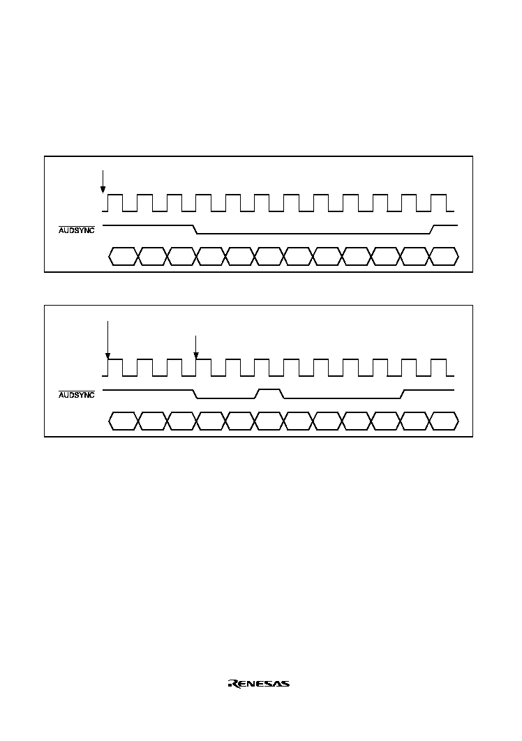
Rev. 2.0, 09/02, page 616 of 732
occur). Note that the compared address is the previous fully output address, and not an interrupted
address (since the upper address of an interrupted address will be unknown).
The interval from the start of execution at the branch destination address in the PC until the
AUDATA pins output 10xx is 1.5 or 2 AUDCK cycles.
AUDCK
0011
0011
1011
A3 to A0 A7 to A4 A11 to A8 A15 to A12 A19 to A16 A23 to A20 A27 to A24 A31 to A28
0011
AUDATA [3:0]
Start of execution at branch destination address in PC
Figure 23.2 Example of Data Output (32-Bit Output)
AUDCK
0011
0011
1011
A3 to A0
0011
0011
A3 to A0 A7 to A4
1010
A7 to A4 A11 to A8 A15 to A12
AUDATA [3:0]
Start of execution at branch destination address in PC (1)
Start of execution at branch destination address in PC (2)
Figure 23.3 Example of Output in Case of Successive Branches
23.4
RAM Monitor Mode
23.4.1
Overview
In this mode, all the modules connected to this LSI's internal or external bus can be read and
written to, allowing RAM monitoring and tuning to be carried out.
When an address is written to AUDATA externally, the data corresponding to that address is
output. If an address and data are written to AUDATA, the data is transferred to the address.
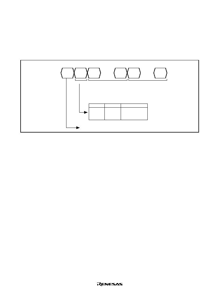
Rev. 2.0, 09/02, page 617 of 732
23.4.2
Communication Protocol
The AUD latches the AUDATA input when
AUDSYNC is asserted. The following AUDATA
input format should be used.
0000
DIR
A3 to A0
A31 to A28 D3 to D0
Dn to Dn-3
Input format
Spare bits (4 bits): b'0000
Command
Fixed at 1
0: Read
1: Write
00: Byte
01: Word
10: Longword
Bit 3
Bit 2
Bit 1
Bit 0
. . . . . .
. . . . . .
Address
Data (in case of write only)
B write: n = 7
W write: n = 15
L write: n = 31
Figure 23.4 AUDATA Input Format
23.4.3
Operation
Operation starts in RAM monitor mode when
AUDRST is asserted, AUDMD is driven high, then
AUDRST is negated.
Figure 23.5 shows an example of a read operation, and figure 23.6 an example of a write
operation.
When
AUDSYNC is asserted, input from the AUDATA pins begins. When a command, address,
or data (writing only) is input in the format shown in figure 23.4, execution of read/write access to
the specified address is started. During internal execution, the AUD returns Not Ready (0000).
When execution is completed, the Ready flag (0001) is returned (figures 23.5 and 23.6). Table
23.2 shows the Ready flag format.
In a read, data of the specified size is output when
AUDSYNC is negated following detection of
this flag (figure 23.5).
If a command other than the above is input in DIR, the AUD treats this as a command error,
disables processing, and sets bit 1 in the Ready flag to 1. If a read/write operation initiated by the
command specified in DIR causes a bus error, the AUD disables processing and sets bit 2 in the
Ready flag to 1 (figure 23.7).
Bus error conditions are shown below.
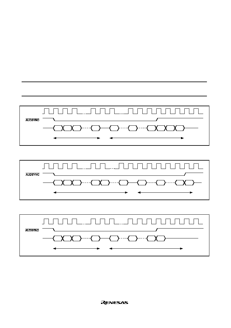
Rev. 2.0, 09/02, page 618 of 732
1. Word access to address 4n+1 or 4n+3
2. Longword access to address 4n+1, 4n+2, or 4n+3
3. Longword access to on-chip I/O 8-bit area
4. Access to external area in single-chip mode
Table 23.2 Ready Flag Format
Bit 3
Bit 2
Bit 1
Bit 0
Fixed at 0
0: Normal status
1: Bus error
0: Normal status
1: Command error
0: Not ready
1: Ready
AUDCK
Not ready
DIR
Ready
Ready Ready
0001
0001
0000
0000
1000
0001
A31 to A28
D7 to D4
D3 to D0
A3 to A0
AUDATAn
Input/output changeover
Input
Output
Figure 23.5 Example of Read Operation (Byte Read)
AUDCK
Not ready
Ready
DIR
Ready Ready
0000
0000
1110
0001
0001
0001
A31 to A28 D3 to D0
D31 to D28
A3 to A0
AUDATAn
Input/output changeover
Input
Output
Figure 23.6 Example of Write Operation (Longword Write)
AUDCK
Not ready
DIR
Ready
(Bus error)
Ready
(Bus error)
Ready
(Bus error)
0101
0101
0000
0000
1010
0101
A31 to A28
A3 to A0
AUDATAn
Input/output changeover
Input
Output
Figure 23.7 Example of Error Occurrence (Longword Read)

Rev. 2.0, 09/02, page 619 of 732
23.5
Usage Notes
23.5.1
Initialization
The debugger's internal buffers and processing states are initialized in the following cases:
1. In a power-on reset
2. When
AUDRST is driven low
3. When the AUDSRST bit in the SYSCR register is cleared to 0 (see section 24.2.2)
4. When the MSTP3 bit in the MSTCR2 register is set to 1 (see section 24.2.3)
23.5.2
Operation in Software Standby Mode
The debugger is not initialized in software standby mode. However, since this LSI's internal
operation halts in software standby mode:
1. When AUDMD is high (RAM monitor mode), Ready is not returned (Not Ready continues to
be returned).
However, when operating on an external clock, the protocol continues.
2.
When AUDMD is low (branch trace mode), operation stops. However, operation continues
when software standby is released.
23.5.3
Setting the PA15/CK pin
Some debug tools have specification that the AUDCK signal is generated out of the CK signal.
Decide the pin function controller setting after reading the manual of the debug tool to be used.
23.5.4
Pin States
1. Module standby
AUDMD
Z
AUDCK
Z
AUDSYNC
Z
AUDATA
Z
2.
AUDRST
=
low-level input
AUDMD
Input
AUDCK
(1) AUDMD
=
high: Input
(2) AUDMD
=
low: High-level Output
AUDSYNC
(1) AUDMD
=
high: Input
(2) AUDMD
=
low: High-level Output
AUDRST
Low-level input
AUDATA
(1) AUDMD
=
high: Input
(2) AUDMD
=
low: High-level Output

Rev. 2.0, 09/02, page 620 of 732
3. Normal operation/software standby
AUDRST
=
1
AUDMD
Input
AUDCK
(1) AUDMD
=
high: Input
(2) AUDMD
=
low: Output
AUDSYNC
(1) AUDMD
=
high: Input
(2) AUDMD
=
low: Output
AUDRST
High-level input
AUDATA
(1) AUDMD
=
high: Input/Output (2) AUDMD
=
low: Output
23.5.5
AUD Start-up Sequence
Follow the sequence described below to start up the AUD.
After selecting the AUD pin by the PFC, input at least three clocks to the AUDCK pin while
retaining the
AUDRST pin at low level. Then, set the AUD reset bit (AUDSRST) in SYSCR to
clear the AUD reset. Low level input to the
AUDRST pin and clock input to the AUDCK pin can
be started prior to the selection of the AUD pin by the PFC.

LPWSH21A_000120020700
Rev. 2.0, 09/02, page 621 of 732
Section 24 Power-Down Modes
In addition to the normal program execution state, this LSI has three power-down modes in which
operation of the CPU and oscillator is halted and power dissipation is reduced. Low-power
operation can be achieved by individually controlling the CPU, on-chip peripheral functions, and
so on.
This LSI's power-down modes are as follows:
∑
Sleep mode
∑
Software standby mode
∑
Module standby mode
Sleep mode indicates the state of the CPU, and module standby mode indicates the state of the on-
chip peripheral function (including the bus master other than the CPU). Some of these states can
be combined.
After a reset, the LSI is in normal-operation mode.
Table 24.1 lists internal operation states in each mode.

Rev. 2.0, 09/02, page 622 of 732
Table 24.1 Internal Operation States in Each Mode
Function
Normal Operation Sleep
Module Standby
Software Standby
System clock pulse generator Functioning
Functioning
Halted
CPU
Functioning
Halted (retained)
Halted (retained)
NMI
Functioning
Functioning
Functioning
External
interrupts
IRQ7
to
IRQ0
UBC
Functioning
Functioning
Halted (reset)
Halted (retained)
DMAC
DTC
Peripheral
functions
IIC
Functioning
Functioning
Halted (reset)
Halted (reset)
I/O port
Functioning
Functioning
Halted (retained)
WDT
Functioning
Functioning
Halted (retained)
SCI
A/D
MTU
CMT
Functioning
Functioning
Halted (reset)
Halted (reset)
H-UDI
Functioning
Functioning
Halted (retained)
Halted (retained)
AUD
ROM
Functioning
Functioning
Halted (reset)
Halted (reset)
RAM
Functioning
Functioning
Halted (retained)
Halted (retained)
Notes: 1. "Halted (retained)" means that the operation of the internal state is suspended, although
internal register values are retained.
2. "Halted (reset)" means that internal register values and internal state are initialized.
3. In module standby mode, only modules for which a stop setting has been made are
halted (reset or retained).
4. There are two types of on-chip peripheral module registers; ones which are initialized
by module standby mode or software standby mode, and those not initialized by that
mode. For details, refer to section 25.3, Register States in Each Operating Mode.
5. The port high-impedance bit (HIZ) in SBYCR sets the state of the I/O port in software
standby mode. For details on the setting, refer to section 24.2.1, Standby Control
Register (SBYCR). For the state of pins, refer to Appendix A, Pin States.

Rev. 2.0, 09/02, page 623 of 732
24.1
Input/Output Pins
Table 24.2 lists the pins relating to power-down mode.
Table 24.2 Pin Configuration
Pin Name
I/O
Function
RES
Input
Power-on reset input pin
MRES
Input
Manual reset input pin
24.2
Register Descriptions
Registers related to power down modes are shown below. For details on register addresses and
register states during each process, refer to section 25, List of Registers.
∑
Standby control register (SBYCR)
∑
System control register (SYSCR)
∑
Module standby control register 1 (MSTCR1)
∑
Module standby control register 2 (MSTCR2)
24.2.1
Standby Control Register (SBYCR)
SBYCR is an 8-bit readable/writable register that performs software standby mode control.
Bit
Bit Name
Initial Value
R/W
Description
7
SSBY
0
R/W
Software Standby
This bit specifies the transition mode after executing
the SLEEP instruction.
0: Shifts to sleep mode after the SLEEP instruction
has been executed
1: Shifts to software standby mode after the SLEEP
instruction has been executed
This bit cannot be set to 1 when the watchdog timer
(WDT) is operating (when the TME bit in TCSR of the
WDT is set to 1). When transferring to software
standby mode, clear the TME bit to 0, stop the WDT,
then set the SSBY bit to 1.

Rev. 2.0, 09/02, page 624 of 732
Bit
Bit Name
Initial Value
R/W
Description
6
HIZ
0
R/W
Port High-Impedance
In software standby mode, this bit selects whether the
pin state of the I/O port is retained or changed to
high-impedance.
0: In software standby mode, the pin state is
retained.
1: In software standby mode, the pin state is
changed to high-impedance.
The HIZ bit cannot be set to 1 when the TME bit in
TCSR of the WDT is set to 1.
When changing the pin state of the I/O port to high-
impedance, clear the TME bit to 0, then set the HIZ
bit to 1.
5
--
0
R
Reserved
This bit is always read as 0, and should always be
written with 0.
4 to 2 --
All 1
R
Reserved
These bits are always read as 1, and should always
be written with 1.
1
IRQEH
1
R/W
IRQ7 to IRQ4 Enable
IRQ7 to IRQ4 interrupts are enabled to clear software
standby mode.
0: Enable to clear the software standby mode
1: Disable to clear the software standby mode
0
IRQEL
1
R/W
IRQ3 to IRQ0 Enable
IRQ3 to IRQ0 interrupts are enabled to clear software
standby mode.
0: Enable to clear the software standby mode
1: Disable to clear the software standby mode

Rev. 2.0, 09/02, page 625 of 732
24.2.2
System Control Register (SYSCR)
SYSCR is an 8-bit readable/writable register that performs AUD software reset control and
enables/disables the access to the on-chip RAM.
Bit
Bit Name
Initial Value
R/W
Description
7, 6
--
All 1
R
Reserved
These bits are always read as 1, and should always
be written with 1.
5 to 2 --
All 0
R
Reserved
These bits are always read as 0, and should always
be written with 0.
1
AUDSRST
0
R/W
AUD Software Reset
This bit controls the AUD reset by software. When 0
is written to AUDSRST, AUD module shifts to power-
on reset state.
0: Shifts to AUD reset state.
1: Clears the AUD reset.
0
RAME
1
R/W
RAM Enable
This bit enables/disables the on-chip RAM.
0: On-chip RAM disabled
1: On-chip RAM enabled
When this bit is cleared to 0, the access the on-chip
RAM is disabled. In this case, an undefined value is
returned when reading or fetching the data or
instruction from the on-chip RAM, and writing to the
on-chip RAM is ignored.
When RAME is cleared to 0 to disable the on-chip
RAM, an instruction to access the on-chip RAM
should not be set next to the instruction to write to
SYSCR. If such an instruction is set, normal access is
not guaranteed.
When RAME is set to 1 to enable the on-chip RAM,
an instruction to read SYSCR should be set next to
the instruction to write to SYSCR. If an instruction to
access the on-chip RAM is set next to the instruction
to write to SYSCR, normal access is not guaranteed.

Rev. 2.0, 09/02, page 626 of 732
24.2.3
Module Standby Control Register 1 and 2 (MSTCR1 and MSTCR2)
MSTCR, comprising two 16-bit readable/writable registers, performs module standby mode
control. Setting a bit to 1, the corresponding module enters module standby mode, while clearing
the bit to 0 clears the module standby mode.
MSTCR1
Bit
Bit Name Initial Value
R/W
Description
15 to 12 --
All 1
R
Reserved
These bits are always read as 1, and should always
be written with 1.
11
MSTP27
0
R/W
On-chip RAM
10
MSTP26
0
R/W
On-chip ROM
9
MSTP25
0
R/W
8
MSTP24
0
R/W
Data transfer controller (DTC)
Direct Memory Access Controller (DMAC)
Set the identical value to MSTP25 and MSTP24,
respectively. When setting module standby, write
b'11, while clearing, write b'00.
7, 6
--
All 0
R
Reserved
These bits are always read as 0, and should always
be written with 0.
5
MSTP21
1
R/W
I
2
C bus interface (IIC)
4
--
1
R
Reserved
These bits are always read as 1, and should always
be written with 1.
3
MSTP19
1
R/W
Serial communication interface 3 (SCI_3)
2
MSTP18
1
R/W
Serial communication interface 2 (SCI_2)
1
MSTP17
1
R/W
Serial communication interface 1 (SCI_1)
0
MSTP16
1
R/W
Serial communication interface 0 (SCI_0)

Rev. 2.0, 09/02, page 627 of 732
MSTCR2
Bit
Bit Name Initial Value
R/W
Description
15, 14
--
All 1
R
Reserved
This bit is always read as 1, and should always be
written with 1.
13
MSTP13
1
R/W
Multi-function timer pulse unit (MTU)
12
MSTP12
1
R/W
Compare match timer (CMT)
11 to 8
--
All 0
R
Reserved
These bits are always read as 0, and should always
be written with 0.
7, 6
--
All 1
R
Reserved
These bits are always read as 1, and should always
be written with 1.
5
MSTP5
1
R/W
A/D converter (A/D1)
4
MSTP4
1
R/W
A/D converter (A/D0)
3
MSTP3
0
R/W
Advanced user debugger (AUD)
*
2
MSTP2
0
R/W
Hitachi user debug interface (H-UDI)
*
1
--
0
R
Reserved
This bit is always read as 0, and should always be
written with 0.
0
MSTP0
0
R/W
User break controller (UBC)
Note:
*
Although this bit can be read from/written to when using E10A (in DBGMD=H), AUD or H-
UDI is in normal operation regardless of the set value.

Rev. 2.0, 09/02, page 628 of 732
24.3
Operation
24.3.1
Sleep Mode
Transition to Sleep Mode: If SLEEP instruction is executed while the SSBY bit in SBYCR = 0,
the CPU enters sleep mode. In sleep mode, CPU operation stops, however the contents of the
CPU's internal registers are retained. Peripheral functions except the CPU do not stop.
In sleep mode, data should not be accessed by the DMAC, DTC, or AUD.
Clearing Sleep Mode: Sleep mode is cleared by the conditions below.
∑
Clearing by the power-on reset
When the
RES pin is driven low, the CPU enters the reset state. When the RES pin is driven
high after the elapse of the specified reset input period, the CPU starts the reset exception
handling.
When an internal Power-on reset by WDT occurs, sleep mode is also cleared.
∑
Clearing by the manual reset
When the
MRES pin is driven low while the RES pin is high, the CPU shifts to the manual
reset state and thus sleep mode is cleared.
When an internal manual reset by WDT occurs, sleep mode is also cleared.

Rev. 2.0, 09/02, page 629 of 732
24.3.2
Software Standby Mode
Transition to Software Standby Mode: A transition is made to software standby mode if the
SLEEP instruction is executed while the SSBY bit in SBYCR is set to 1. In this mode, the CPU,
on-chip peripheral functions, and the oscillator, all stop.
However, the contents of the CPU's internal registers and on-chip RAM data (when the RAME bit
in SYSCR is 0) are retained as long as the specified voltage is supplied. There are two types of on-
chip peripheral module registers; ones which are initialized by software standby mode, and those
not initialized by that mode. For details, refer to section 25.3, Register States in Each Operating
Mode. The port high-impedance bit (HIZ) in SBYCR sets the state of the I/O port either to
"retained" or "high-impedance". For the state of pins, refer to Appendix A, Pin States. In software
standby mode, the oscillator stops and thus power consumption is significantly reduced.
Clearing Software Standby Mode: Software standby mode is cleared by the condition below.
∑
Clearing by the NMI interrupt input
When the falling edge or rising edge of the NMI pin (selected by the NMI edge select bit
(NMIE) in ICR1 of the interrupt controller (INTC)) is detected, clock oscillation is started.
This clock pulse is supplied only to the watchdog timer (WDT).
After the elapse of the time set in the clock select bits (CKS2 to CKS0) in TCSR of the WDT
before the transition to software standby mode, the WDT overflow occurs. Since this overflow
indicates that the clock has been stabilized, clock pulse will be supplied to the entire chip after
this overflow. Software standby mode is thus cleared and the NMI exception handling is
started.
When clearing software standby mode by the NMI interrupt, set CKS2 to CKS0 bits so that the
WDT overflow period will be longer than the oscillation stabilization time.
When so&tware standby mode is cleared by the falling edge of the NMI pin, the NMI pin
should be high when the CPU enters software standby mode (when the clock pulse stops) and
should be low when the CPU returns from standby mode (when the clock is initiated after the
oscillation stabilization). When software standby mode is cleared by the rising edge of the
NMI pin, the NMI pin should be low when the CPU enters software standby mode (when the
clock pulse stops) and should be high when the CPU returns from software standby mode
(when the clock is initiated after the oscillation stabilization).
∑
Clearing by the
RES pin
When the
RES pin is driven low, clock oscillation is started. At the same time as clock
oscillation is started, clock pulse is supplied to the entire chip. Ensure that the
RES pin is held
low until clock oscillation stabilizes. When the
RES pin is driven high, the CPU starts the reset
exception handling.

Rev. 2.0, 09/02, page 630 of 732
∑
Clearing by the IRQ interrupt input
When the falling edge or rising edge of the
IRQ pin (selected by the IRQ7S to IRQ0S bits in
ICR1 of the interrupt controller (INTC) and the IRQ7ES[1:0] to IRQ0ES[1:0] bits in ICR2) is
detected, clock oscillation is started*. This clock pulse is supplied only to the watchdog timer
(WDT). The IRQ interrupt priority level should be higher than the interrupt mask level set in
the status register (SR) of the CPU before the transition to software standby mode.
After the elapse of the time set in the clock select bits (CKS2 to CKS0) in TCSR of the WDT
before the transition to software standby mode, the WDT overflow occurs. Since this overflow
indicates that the clock has been stabilized, clock pulse will be supplied to the entire chip after
this overflow. Software standby mode is thus cleared and the IRQ exception handling is
started.
When clearing software standby mode by the IRQ interrupt, set CKS2 to CKS0 bits so that the
WDT overflow period will be longer than the oscillation stabilization time.
When software standby mode is cleared by the falling edge or both rising and falling edges of
the
IRQ pin, the IRQ pin should be high when the CPU enters software standby mode (when
the clock pulse stops) and should be low when the CPU returns from software standby mode
(when the clock is initiated after the oscillation stabilization). When software standby mode is
cleared by the rising edge of the
IRQ pin, the IRQ pin should be low when the CPU enters
software standby mode (when the clock pulse stops) and should be high when the CPU returns
from software standby mode (when the clock is initiated after the oscillation stabilization).
Note: * If the
IRQ pin setting is detection at the falling edge or detection at both rising and falling
edges, clock oscillation starts at the falling edge detection. If the setting is detection at the
rising edge, it starts at the rising edge detection. Do not set the
IRQ pin to detection at the
low level.
Software Standby Mode Application Example: Figure 24.1 shows an example in which a
transition is made to software standby mode at the falling edge of the NMI pin, and software
standby mode is cleared at a rising edge of the NMI pin.
In this example, when the NMI pin is driven low while the NMI edge select bit (NMIE) in ICR1 is
0 (falling edge specification), an NMI interrupt is accepted. Then, the NMIE bit is set to 1 (rising
edge specification) in the NMI exception service routine, the SSBY bit in SBYCR is set to 1, and
a SLEEP instruction is executed to transfer to software standby mode.
Software standby mode is cleared at the rising edge of the NMI pin.
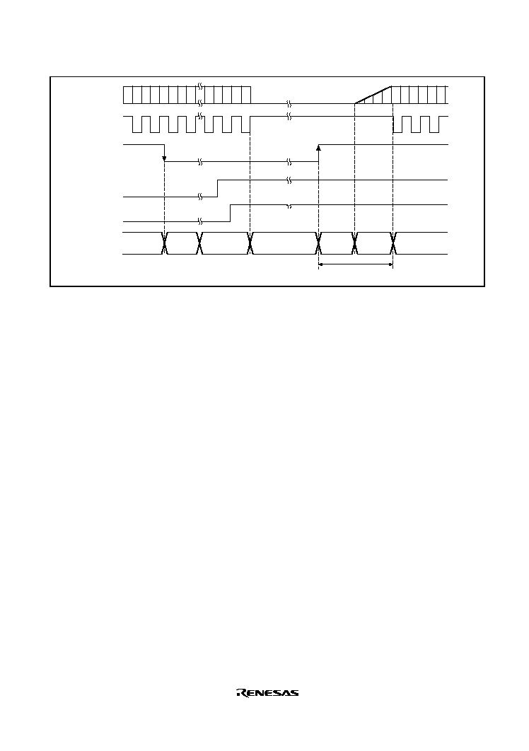
Rev. 2.0, 09/02, page 631 of 732
Oscillator
CK
NMI input
NMIE bit
SSBY bit
LSI state
Oscillation
start time
Program
execution state
Exception
service routine
Software
standby mode
WDT
setting time
NMI exception
handling
NMI
exception
handling
Oscillation stabilization
time
Figure 24.1 NMI Timing in Software Standby Mode (Application Example)
24.3.3
Module Standby Mode
Module standby mode can be set for individual on-chip peripheral functions.
When the corresponding MSTP bit in MSTCR is set to 1, module operation stops at the end of the
bus cycle and a transition is made to module standby mode. The CPU continues operating
independently.
When the corresponding MSTP bit is cleared to 0, module standby mode is cleared and the
module starts operating at the end of the bus cycle. In some of the modules that have entered
module standby mode, register values are initialized. Therefore, set registers again when operating
the modules.
After reset clearing, the I
2
C, SCI, MTU, CMT, and A/D converter are in module standby mode.
The modules of registers in module standby mode cannot be read or written to.

Rev. 2.0, 09/02, page 632 of 732
24.4
Usage Notes
24.4.1
I/O Port Status
When a transition is made to software standby mode while the port high-impedance bit (HIZ) in
SBYCR is 0, I/O port states are retained. Therefore, there is no reduction in current consumption
for the output current when a high-level signal is output.
24.4.2
Current Consumption during Oscillation Stabilization Wait Period
Current consumption increases during the oscillation stabilization wait period.
24.4.3
On-Chip Peripheral Module Interrupt
Relevant interrupt operations cannot be performed in module standby mode. Consequently, if the
CPU enters module standby mode while an interrupt has been requested, it will not be possible to
clear the CPU interrupt source or the DMAC/DTC activation source.
Interrupts should therefore be disabled before entering module standby mode.
24.4.4
Writing to MSTCR1 and MSTCR2
MSTCR1 and MSTCR2 should only be written to by the CPU.
24.4.5
DMAC, DTC, or AUD Operation in Sleep Mode
In sleep mode, data should not be accessed by the DMAC, DTC, or AUD.

Rev. 2.0, 09/02, page 633 of 732
Section 25 List of Registers
This section gives information on internal I/O registers. The contents of this section are as follows:
1. Register Address Table (in the order from a lower address)
∑
Registers are listed in the order from lower allocated addresses.
∑
As for reserved addresses, the register name column is indicated with
. Do not access
reserved addresses.
∑
As for 16- or 32-bit address, the MSB addresses are shown.
∑
The list is classified according to module names.
2. Register Bit Table
∑
Bit configurations are shown in the order of the register address table.
∑
As for reserved bits, the bit name column is indicated with
.
∑
As for the blank column of the bit names, the whole register is allocated to the counter or data.
∑
As for 16- or 32-bit registers, bits are indicated from the MSB.
3. Register State in Each Operating Mode
∑
Register states are listed in the order of the register address table.
∑
Register states in the basic operating mode are shown. As for modules including their specific
states such as reset, see the sections of those modules.
25.1
Register Address Table (In the Order from Lower Addresses)
Access sizes are indicated with the number of bits. Access states are indicated with the number of
specified reference clock states. These values are those at 8-bit access (B), 16-bit access (W), or
32-bit access (L).
Note:
Access to undefined or reserved addresses is prohibited. Correct operation cannot be
guaranteed if these addresses are accessed.

Rev. 2.0, 09/02, page 634 of 732
Register name
abbreviation
NO. of
bits
Address
Module
Access size
NO. of Access
states
H'FFFF8000 to
H'FFFF819F
Serial mode register_0
SMR_0
8
H'FFFF81A0
SCI
8, 16
P
reference
Bit rate register_0
BRR_0
8
H'FFFF81A1
(Channel 0)
8
B:2
Serial control register_0
SCR_0
8
H'FFFF81A2
8, 16
W:4
Transmit data register_0
TDR_0
8
H'FFFF81A3
8
Serial status register_0
SSR_0
8
H'FFFF81A4
8, 16
Receive data register_0
RDR_0
8
H'FFFF81A5
8
Serial direction control register_0
SDCR_0
8
H'FFFF81A6
8
H'FFFF81A7 to
H'FFFF81AF
Serial mode register_1
SMR_1
8
H'FFFF81B0
SCI
8, 16
Bit rate register_1
BRR_1
8
H'FFFF81B1
(Channel 1)
8
Serial control register_1
SCR_1
8
H'FFFF81B2
8, 16
Transmit data register_1
TDR_1
8
H'FFFF81B3
8
Serial status register_1
SSR_1
8
H'FFFF81B4
8, 16
Receive data register_1
RDR_1
8
H'FFFF81B5
8
Serial direction control register_1
SDCR_1
8
H'FFFF81B6
8
H'FFFF81B7 to
H'FFFF81BF
Serial mode register_2
SMR_2
8
H'FFFF81C0
SCI
8, 16
Bit rate register_2
BRR_2
8
H'FFFF81C1
(Channel 2)
8
Serial control register_2
SCR_2
8
H'FFFF81C2
8, 16
Transmit data register_2
TDR_2
8
H'FFFF81C3
8
Serial status register_2
SSR_2
8
H'FFFF81C4
8, 16
Receive data register_2
RDR_2
8
H'FFFF81C5
8
Serial direction control register_2
SDCR_2
8
H'FFFF81C6
8
H'FFFF81C7 to
H'FFFF81CF
Serial mode register_3
SMR_3
8
H'FFFF81D0
SCI
8, 16
Bit rate register_3
BRR_3
8
H'FFFF81D1
(Channel 3)
8
Serial control register_3
SCR_3
8
H'FFFF81D2
8, 16
Transmit data register_3
TDR_3
8
H'FFFF81D3
8

Rev. 2.0, 09/02, page 635 of 732
Register name
abbreviation
NO. of
bits
Address
Module
Access size
NO. of Access
states
Serial status register_3
SSR_3
8
H'FFFF81D4
8, 16
P
reference
Receive data register_3
RDR_3
8
H'FFFF81D5
8
B:2
Serial direction control register_3
SDCR_3
8
H'FFFF81D6
8
W:4
H'FFFF81D7 to
H'FFFF81FF
Timer control register_3
TCR_3
8
H'FFFF8200
MTU
8, 16, 32
P
reference
Timer control register_4
TCR_4
8
H'FFFF8201
(Channels 3, 4)
8
B:2
Timer mode register_3
TMDR_3
8
H'FFFF8202
8, 16
W:2
Timer mode register_4
TMDR_4
8
H'FFFF8203
8
L:4
Timer I/O control register H_3
TIORH_3
8
H'FFFF8204
8, 16, 32
Timer I/O control register L_3
TIORL_3
8
H'FFFF8205
8
Timer I/O control register H_4
TIORH_4
8
H'FFFF8206
8, 16
Timer I/O control register L_4
TIORL_4
8
H'FFFF8207
8
Timer interrupt enable register_3
TIER_3
8
H'FFFF8208
8, 16, 32
Timer interrupt enable register_4
TIER_4
8
H'FFFF8209
8
Timer output master enable register
TOER
8
H'FFFF820A
8, 16
Timer output control register
TOCR
8
H'FFFF820B
8
H'FFFF820C
Timer gate control register
TGCR
8
H'FFFF820D
8
H'FFFF820E
H'FFFF820F
Timer counter_3
TCNT_3
16
H'FFFF8210
16, 32
Timer counter_4
TCNT_4
16
H'FFFF8212
16
Timer cyclic data register
TCDR
16
H'FFFF8214
16, 32
Timer dead time data register
TDDR
16
H'FFFF8216
16
Timer general register A_3
TGRA_3
16
H'FFFF8218
16, 32
Timer general register B_3
TGRB_3
16
H'FFFF821A
16
Timer general register A_4
TGRA_4
16
H'FFFF821C
16, 32
Timer general register B_4
TGRB_4
16
H'FFFF821E
16
Timer sub-counter
TCNTS
16
H'FFFF8220
16, 32
Timer cyclic buffer register
TCBR
16
H'FFFF8222
16

Rev. 2.0, 09/02, page 636 of 732
Register name
abbreviation
NO. of
bits
Address
Module
Access size
NO. of Access
states
Timer general register C_3
TGRC_3
16
H'FFFF8224
MTU
16, 32
P
reference
Timer general register D_3
TGRD_3
16
H'FFFF8226
(Channels 3, 4)
16
B:2
Timer general register C_4
TGRC_4
16
H'FFFF8228
16, 32
W:2
Timer general register D_4
TGRD_4
16
H'FFFF822A
16
L:4
Timer status register_3
TSR_3
8
H'FFFF822C
8, 16
Timer status register_4
TSR_4
8
H'FFFF822D
8
H'FFFF822E to
H'FFFF823F
Timer start register
TSTR
8
H'FFFF8240
MTU
(for all channels)
8, 16
P
reference
B:2
Timer synchronous register
TSYR
8
H'FFFF8241
8
W:2
H'FFFF8242 to
H'FFFF825F
Timer control register_0
TCR_0
8
H'FFFF8260
MTU
8, 16, 32
P
reference
Timer mode register_0
TMDR_0
8
H'FFFF8261
(Channel 0)
8
B:2
Timer I/O control register H_0
TIORH_0
8
H'FFFF8262
8, 16
W:2
Timer I/O control register L_0
TIORL_0
8
H'FFFF8263
8
L:4
Timer interrupt enable register_0
TIER_0
8
H'FFFF8264
8, 16, 32
Timer status register_0
TSR_0
8
H'FFFF8265
8
Timer counter_0
TCNT_0
16
H'FFFF8266
16
Timer general register A_0
TGRA_0
16
H'FFFF8268
16, 32
Timer general register B_0
TGRB_0
16
H'FFFF826A
16
Timer general register C_0
TGRC_0
16
H'FFFF826C
16, 32
Timer general register D_0
TGRD_0
16
H'FFFF826E
16
H'FFFF8270 to
H'FFFF827F

Rev. 2.0, 09/02, page 637 of 732
Register name
abbreviation
NO. of
bits
Address
Module
Access size
NO. of Access
states
Timer control register_1
TCR_1
8
H'FFFF8280
MTU
8, 16
P
reference
Timer mode register_1
TMDR_1
8
H'FFFF8281
(Channel 1)
8
B:2
Timer I/O control register_1
TIOR_1
8
H'FFFF8282
8
W:2
H'FFFF8283
L:4
Timer interrupt enable register_1
TIER_1
8
H'FFFF8284
8, 16, 32
Timer status register_1
TSR_1
8
H'FFFF8285
8
Timer counter_1
TCNT_1
16
H'FFFF8286
16
Timer general register A_1
TGRA_1
16
H'FFFF8288
16, 32
Timer general register B_1
TGRB_1
16
H'FFFF828A
16
H'FFFF828C to
H'FFFF829F
Timer control register_2
TCR_2
8
H'FFFF82A0
MTU(Channel 2) 8, 16
Timer mode register_2
TMDR_2
8
H'FFFF82A1
MTU
8
Timer I/O control register_2
TIOR_2
8
H'FFFF82A2
(Channel 2)
8
H'FFFF82A3
Timer interrupt enable register_2
TIER_2
8
H'FFFF82A4
8, 16, 32
Timer status register_2
TSR_2
8
H'FFFF82A5
8
Timer counter_2
TCNT_2
16
H'FFFF82A6
16
Timer general register A_2
TGRA_2
16
H'FFFF82A8
16, 32
Timer general register B_2
TGRB_2
16
H'FFFF82AA
16
H'FFFF82AC to
H'FFFF833F

Rev. 2.0, 09/02, page 638 of 732
Register name
abbreviation
NO. of
bits
Address
Module
Access size
NO. of Access
states
H'FFFF8340 to
H'FFFF8347
INTC
reference
B:2
Interrupt priority register A
IPRA
16
H'FFFF8348
8, 16, 32
W:2
Interrupt priority register B
IPRB
16
H'FFFF834A
8, 16
L:4
Interrupt priority register C
IPRC
16
H'FFFF834C
8, 16, 32
Interrupt priority register D
IPRD
16
H'FFFF834E
8, 16
Interrupt priority register E
IPRE
16
H'FFFF8350
8, 16, 32
Interrupt priority register F
IPRF
16
H'FFFF8352
8, 16
Interrupt priority register G
IPRG
16
H'FFFF8354
8, 16, 32
Interrupt priority register H
IPRH
16
H'FFFF8356
8, 16
Interrupt control register1
ICR1
16
H'FFFF8358
8, 16, 32
IRQ status register
ISR
16
H'FFFF835A
8, 16
Interrupt priority register I
IPRI
16
H'FFFF835C
8, 16, 32
Interrupt priority register J
IPRJ
16
H'FFFF835E
8, 16
H'FFFF8360 to
H'FFFF8365
Interrupt control register 2
ICR2
16
H'FFFF8366
8, 16
H'FFFF8368 to
H'FFFF837F
Port A data register H
PADRH
16
H'FFFF8380
I/O
8, 16, 32
Port A data register L
PADRL
16
H'FFFF8382
8, 16
Port A I/O register H
PAIORH
16
H'FFFF8384
PFC
8, 16, 32
Port A I/O register L
PAIORL
16
H'FFFF8386
8, 16
Port A control register H
PACRH
16
H'FFFF8388
8, 16, 32
H'FFFF838A
Port A control register L1
PACRL1
16
H'FFFF838C
8, 16, 32
Port A control register L2
PACRL2
16
H'FFFF838E
8, 16
Port B data register
PBDR
16
H'FFFF8390
I/O
8, 16, 32
Port C data register
PCDR
16
H'FFFF8392
8, 16
Port B I/O register
PBIOR
16
H'FFFF8394
PFC
8, 16, 32
Port C I/O register
PCIOR
16
H'FFFF8396
8, 16

Rev. 2.0, 09/02, page 639 of 732
Register name
abbreviation
NO. of
bits
Address
Module
Access size
NO. of Access
states
Port B control register 1
PBCR1
16
H'FFFF8398
PFC
8, 16, 32
reference
Port B control register 2
PBCR2
16
H'FFFF839A
8, 16
B:2
Port C control register 2
PCCR
16
H'FFFF839C
8, 16, 32
H'FFFF839E to
H'FFFF839F
W:2
L:4
Port D data register H
PDDRH
16
H'FFFF83A0
I/O
8, 16, 32
Port D data register L
PDDRL
16
H'FFFF83A2
8, 16
Port D I/O register H
PDIORH
16
H'FFFF83A4
PFC
8, 16, 32
Port D I/O register L
PDIORL
16
H'FFFF83A6
8, 16
Port D control register H1
PDCRH1
16
H'FFFF83A8
8, 16, 32
Port D control register H2
PDCRH2
16
H'FFFF83AA
8, 16
Port D control register L1
PDCRL1
16
H'FFFF83AC
8, 16, 32
Port D control register L2
PDCRL2
16
H'FFFF83AE
8, 16
Port E data register L
PEDRL
16
H'FFFF83B0
I/O
8, 16, 32
H'FFFF83B2
Port F data register
PFDR
8
H'FFFF83B3
I/O
8
Port E I/O register L
PEIORL
16
H'FFFF83B4
PFC
8, 16, 32
H'FFFF83B6 to
H'FFFF83B7
Port E control register L1
PECRL1
16
H'FFFF83B8
PFC
8, 16, 32
Port E control register L2
PECRL2
16
H'FFFF83BA
8, 16
H'FFFF83BC to
H'FFFF83BF
Input control/status register 1
ICSR1
16
H'FFFF83C0
POE
8, 16, 32
Output control/status register
OCSR
16
H'FFFF83C2
8, 16
P
reference
B:2
H'FFFF83C4 to
H'FFFF83CF
W:2
L:4

Rev. 2.0, 09/02, page 640 of 732
Register name
abbreviation
NO. of
bits
Address
Module
Access size
NO. of Access
states
Compare match timer start register
CMSTR
16
H'FFFF83D0
CMT
8, 16, 32
Compare match timer control
/status register_0
CMCSR_0
16
H'FFFF83D2
8, 16
P
reference
B:2
W:2
Compare match timer counter_0
CMCNT_0
16
H'FFFF83D4
8, 16, 32
Compare match timer constant register_0
CMCOR_0
16
H'FFFF83D6
8, 16
L:4
Compare match timer control
/status register_1
CMCSR_1
16
H'FFFF83D8
8, 16, 32
Compare match timer counter_1
CMCNT_1
16
H'FFFF83DA
8, 16
Compare match timer constant register_1
CMCOR_1
16
H'FFFF83DC
8, 16
H'FFFF83DE to
H'FFFF841F
A/D data register 0
ADDR0
16
H'FFFF8420
A/D
8, 16
A/D data register 1
ADDR1
16
H'FFFF8422
(Channel0)
8, 16
A/D data register 2
ADDR2
16
H'FFFF8424
8, 16
A/D data register 3
ADDR3
16
H'FFFF8426
8, 16
A/D data register 4
ADDR4
16
H'FFFF8428
A/D
8, 16
A/D data register 5
ADDR5
16
H'FFFF842A
(Channel1)
8, 16
A/D data register 6
ADDR6
16
H'FFFF842C
8, 16
A/D data register 7
ADDR7
16
H'FFFF842E
8, 16
H'FFFF8430 to
H'FFFF847F
A/D control/status register_0
ADCSR_0
8
H'FFFF8480
A/D
8, 16
A/D control/status register_1
ADCSR_1
8
H'FFFF8481
8
H'FFFF8482 to
H'FFFF8487
A/D control register_0
ADCR_0
8
H'FFFF8488
A/D
8, 16
A/D control register_1
ADCR_1
8
H'FFFF8489
8
P
reference
B:3
W:6
H'FFFF848A to
H'FFFF857F

Rev. 2.0, 09/02, page 641 of 732
Register name
abbreviation
NO. of
bits
Address
Module
Access size
NO. of Access
states
Flash memory control register 1
FLMCR1
8
H'FFFF8580
FLASH
8, 16
reference
Flash memory control register 2
FLMCR2
8
H'FFFF8581
(Only in F-ZTAT
version)
8
B:3
W:6
Erase block register 1
EBR1
8
H'FFFF8582
8, 16
Erase block register 2
EBR2
8
H'FFFF8583
8
H'FFFF8584 to
H'FFFF85FF
User break address register H
UBARH
16
H'FFFF8600
UBC
8, 16, 32
User break address register L
UBARL
16
H'FFFF8602
8, 16
User break address mask register H
UBAMRH
16
H'FFFF8604
8, 16, 32
User break address mask register L
UBAMRL
16
H'FFFF8606
8, 16
User break bus cycle register
UBBR
16
H'FFFF8608
8, 16, 32
User break control register
UBCR
16
H'FFFF860A
8, 16
reference
B:3
W:3
L:6
H'FFFF860C to
H'FFFF860F
Timer control/status register
TCSR
8
H'FFFF8610
WDT
8
*
2
/16
*
1
reference
Timer counter
TCNT
*
1
8
H'FFFF8610
*
1: Write
16
B:3
Timer counter
TCNT
*
2
8
H'FFFF8611
*
2: Read
8
W:3
Reset control/status register
RSTCSR
*
1
8
H'FFFF8612
16
Reset control/status register
RSTCSR
*
2
8
H'FFFF8613
8
Standby control register
SBYCR
8
H'FFFF8614
Power-down
modes
8
reference
B:3
H'FFFF8615 to
H'FFFF8617
System control register
SYSCR
8
H'FFFF8618
8
H'FFFF8619 to
H'FFFF861B
Power-down
modes
Module standby control register 1
MSTCR1
16
H'FFFF861C
8, 16, 32
Module standby control register 2
MSTCR2
16
H'FFFF861E
8, 16
P
reference
B:3
W:3
L:6

Rev. 2.0, 09/02, page 642 of 732
Register name
abbreviation
NO. of
bits
Address
Module
Access size
NO. of Access
states
Bus control register 1
BCR1
16
H'FFFF8620
BSC
8, 16, 32
Bus control register 2
BCR2
16
H'FFFF8622
8, 16
Wait control register 1
WCR1
16
H'FFFF8624
8, 16, 32
Wait control register 2
WCR2
16
H'FFFF8626
8, 16
reference
B:3
W:3
L:6
RAM emulation register
RAMER
16
H'FFFF8628
FLASH
(Only in F-ZTAT
version)
8, 16
reference
B:3
W:3
H'FFFF862A to
H'FFFF86AF
DMA operation register
DMAOR
16
H'FFFF86B0
8, 16
reference
H'FFFF86B2 to
H'FFFF86BF
DMAC
(for all channels)
W:3
L:6
DMA source address register_0
SAR_0
32
H'FFFF86C0
DMAC
8, 16, 32
DMA destination address register_0
DAR_0
32
H'FFFF86C4
(Channel 0)
8, 16, 32
DMA transfer count register_0
DMATCR_0
32
H'FFFF86C8
8, 16, 32
DMA channel control register_0
CHCR_0
32
H'FFFF86CC
8, 16, 32
DMA source address register_1
SAR_1
32
H'FFFF86D0
DMAC
8, 16, 32
DMA destination address register_1
DAR_1
32
H'FFFF86D4
(Channel 1)
8, 16, 32
DMA transfer count register_1
DMATCR_1
32
H'FFFF86D8
8, 16, 32
DMA channel control register_1
CHCR_1
32
H'FFFF86DC
8, 16, 32
DMA source address register_2
SAR_2
32
H'FFFF86E0
DMAC
8, 16, 32
DMA destination address register_2
DAR_2
32
H'FFFF86E4
(Channel 2)
8, 16, 32
DMA transfer count register_2
DMATCR_2
32
H'FFFF86E8
8, 16, 32
DMA channel control register_2
CHCR_2
32
H'FFFF86EC
8, 16, 32
DMA source address register_3
SAR_3
32
H'FFFF86F0
DMAC
8, 16, 32
DMA destination address register_3
DAR_3
32
H'FFFF86F4
(Channel 3)
8, 16, 32
DMA transfer count register_3
DMATCR_3
32
H'FFFF86F8
8, 16, 32
DMA channel control register_3
CHCR_3
32
H'FFFF86FC
8, 16, 32

Rev. 2.0, 09/02, page 643 of 732
Register name
abbreviation
NO. of
bits
Address
Module
Access size
NO. of Access
states
DTC enable register A
DTEA
8
H'FFFF8700
DTC
8, 16, 32
reference
DTC enable register B
DTEB
8
H'FFFF8701
8
DTC enable register C
DTEC
8
H'FFFF8702
8, 16
DTC enable register D
DTED
8
H'FFFF8703
8
B:3
W:3
L:6
H'FFFF8704 to
H'FFFF8705
DTC control/status register
DTCSR
16
H'FFFF8706
8, 16, 32
DTC information base register
DTBR
16
H'FFFF8708
8, 16
H'FFFF870A to
H'FFFF870F
DTC enable register E
DTEE
8
H'FFFF8710
8, 16
H'FFFF8711
DTC enable register G
DTEG
8
H'FFFF8712
8, 16
H'FFFF8713 to
H'FFFF87EF
Serial control register X
SCRX
8
H'FFFF87F0
I
2
C
[Option]
8
P
reference
B:3
H'FFFF87F1 to
H'FFFF87F3
AD trigger select register
ADTSR
8
H'FFFF87F4
A/D
8
P
reference
B:3
H'FFFF87F5 to
H'FFFF87F7
High-current port control register
PPCR
8
H'FFFF87F8
Port E
8
P
reference
B:3
H'FFFF87F9 to
H'FFFF8807

Rev. 2.0, 09/02, page 644 of 732
Register name
abbreviation
NO. of
bits
Address
Module
Access size
NO. of Access
states
I
2
C bus control register
ICCR
8
H'FFFF8808
I
2
C
8, 16
I
2
C bus status register
ICSR
8
H'FFFF8809
[Option]
8
H'FFFF880A to
H'FFFF880D
I
2
C bus data register
ICDR
8
H'FFFF880E
*
8, 16
P
reference
B:2
W:4
Second slave address register
SARX
8
H'FFFF880E
*
8, 16
I
2
C bus mode register
ICMR
8
H'FFFF880F
*
8
Slave address register
SAR
8
H'FFFF880F
*
8
H'FFFF8810 to
H'FFFF8A4F
Instruction register
SDIR
16
H'FFFF8A50
H-UDI
(Only in F-ZTAT
version)
8, 16, 32
P
reference
B:2
W:2
Status register
SDSR
16
H'FFFF8A52
8, 16
L:4
Data register H
SDDRH
16
H'FFFF8A54
8, 16, 32
Data register L
SDDRL
16
H'FFFF8A56
8, 16
H'FFFF8A58 to
H'FFFFBFFF
Note: * Registers that can be read from/written to differ according to the setting of the ICE bit in
the IIC bus control register 0. In ICE=0, the registers read from/written to are the second
slave address register 0 and the slave address register 0. In ICE=1, they are the IIC bus
data register 0 and the IIC bus mode register 0.

Rev. 2.0, 09/02, page 645 of 732
25.2
Register Bit List
Addresses and bit names of each on-chip peripheral module are shown below.
As for 16-bit or 32-bit registers, they are shown in two or four rows.
Register
abbreviation
Bit7
Bit6
Bit5
Bit4
Bit3
Bit2
Bit1
Bit0
Module
SMR_0
C/
A
CHR
PE
O/
E
STOP
MP
CKS1
CKS0
BRR_0
SCR_0
TIE
RIE
TE
RE
MPIE
TEIE
CKE1
CKE0
TDR_0
SSR_0
TDRE
RDRF
ORER
FER
PER
TEND
MPB
MPBT
SCI
(Channel 0)
RDR_0
SDCR_0
DIR
SMR_1
C/
A
CHR
PE
O/
E
STOP
MP
CKS1
CKS0
BRR_1
SCR_1
TIE
RIE
TE
RE
MPIE
TEIE
CKE1
CKE0
TDR_1
SSR_1
TDRE
RDRF
ORER
FER
PER
TEND
MPB
MPBT
SCI
(Channel 1)
RDR_1
SDCR_1
DIR
SMR_2
C/
A
CHR
PE
O/
E
STOP
MP
CKS1
CKS0
BRR_2
SCR_2
TIE
RIE
TE
RE
MPIE
TEIE
CKE1
CKE0
TDR_2
SSR_2
TDRE
RDRF
ORER
FER
PER
TEND
MPB
MPBT
SCI
(Channel 2)
RDR_2
SDCR_2
DIR

Rev. 2.0, 09/02, page 646 of 732
Register
abbreviation
Bit7
Bit6
Bit5
Bit4
Bit3
Bit2
Bit1
Bit0
Module
SMR_3
C/
A
CHR
PE
O/
E
STOP
MP
CKS1
CKS0
BRR_3
SCR_3
TIE
RIE
TE
RE
MPIE
TEIE
CKE1
CKE0
TDR_3
SSR_3
TDRE
RDRF
ORER
FER
PER
TEND
MPB
MPBT
SCI
(Channel 3)
RDR_3
SDCR_3
DIR
TCR_3
CCLR2
CCLR1
CCLR0
CKEG1
CKEG0
TPSC2
TPSC1
TPSC0
TCR_4
CCLR2
CCLR1
CCLR0
CKEG1
CKEG0
TPSC2
TPSC1
TPSC0
TMDR_3
BFB
BFA
MD3
MD2
MD1
MD0
TMDR_4
BFB
BFA
MD3
MD2
MD1
MD0
MTU
(Channels 3, 4)
TIORH_3
IOB3
IOB2
IOB1
IOB0
IOA3
IOA2
IOA1
IOA0
TIORL_3
IOD3
IOD2
IOD1
IOD0
IOC3
IOC2
IOC1
IOC0
TIORH_4
IOB3
IOB2
IOB1
IOB0
IOA3
IOA2
IOA1
IOA0
TIORL_4
IOD3
IOD2
IOD1
IOD0
IOC3
IOC2
IOC1
IOC0
TIER_3
TTGE
TCIEV
TGIED
TGIEC
TGIEB
TGIEA
TIER_4
TTGE
TCIEV
TGIED
TGIEC
TGIEB
TGIEA
TOER
OE4D
OE4C
OE3D
OE4B
OE4A
OE3B
TOCR
PSYE
OLSN
OLSP
TGCR
BDC
N
P
FB
WF
VF
UF
TCNT_3
TCNT_4
TCDR
TDDR

Rev. 2.0, 09/02, page 647 of 732
Register
abbreviation
Bit7
Bit6
Bit5
Bit4
Bit3
Bit2
Bit1
Bit0
Module
TGRA_3
TGRB_3
TGRA_4
TGRB_4
MTU
(Channels 3, 4)
TCNTS
TCBR
TGRC_3
TGRD_3
TGRC_4
TGRD_4
TSR_3
TCFD
TCFV
TGFD
TGFC
TGFB
TGFA
TSR_4
TCFD
TCFV
TGFD
TGFC
TGFB
TGFA
TSTR
CST4
CST3
CST2
CST1
CST0
TSYR
SYNC4
SYNC3
SYNC2
SYNC1
SYNC0

Rev. 2.0, 09/02, page 648 of 732
Register
abbreviation
Bit7
Bit6
Bit5
Bit4
Bit3
Bit2
Bit1
Bit0
Module
TCR_0
CCLR2
CCLR1
CCLR0
CKEG1
CKEG0
TPSC2
TPSC1
TPSC0
TMDR_0
BFB
BFA
MD3
MD2
MD1
MD0
MTU
(Channel 0)
TIORH_0
IOB3
IOB2
IOB1
IOB0
IOA3
IOA2
IOA1
IOA0
TIORL_0
IOD3
IOD2
IOD1
IOD0
IOC3
IOC2
IOC1
IOC0
TIER_0
TTGE
TCIEV
TGIED
TGIEC
TGIEB
TGIEA
TSR_0
TCFV
TGFD
TGFC
TGFB
TGFA
TCNT_0
TGRA_0
TGRB_0
TGRC_0
TGRD_0
TCR_1
CCLR1
CCLR0
CKEG1
CKEG0
TPSC2
TPSC1
TPSC0
TMDR_1
MD3
MD2
MD1
MD0
TIOR_1
IOB3
IOB2
IOB1
IOB0
IOA3
IOA2
IOA1
IOA0
TIER_1
TTGE
TCIEU
TCIEV
TGIEB
TGIEA
TSR_1
TCFD
TCFU
TCFV
TGFB
TGFA
TCNT_1
TGRA_1
TGRB_1
MTU
(Channel 1)
TCR_2
CCLR1
CCLR0
CKEG1
CKEG0
TPSC2
TPSC1
TPSC0
TMDR_2
MD3
MD2
MD1
MD0
TIOR_2
IOB3
IOB2
IOB1
IOB0
IOA3
IOA2
IOA1
IOA0
TIER_2
TTGE
TCIEU
TCIEV
TGIEB
TGIEA
TSR_2
TCFD
TCFU
TCFV
TGFB
TGFA
MTU
(Channel 2)

Rev. 2.0, 09/02, page 649 of 732
Register
abbreviation
Bit7
Bit6
Bit5
Bit4
Bit3
Bit2
Bit1
Bit0
Module
TCNT_2
TGRA_2
TGRB_2
MTU
(Channel 2)
IRQ0
IRQ0
IRQ0
IRQ0
IRQ1
IRQ1
IRQ1
IRQ1
IPRA
IRQ2
IRQ2
IRQ2
IRQ2
IRQ3
IRQ3
IRQ3
IRQ3
IRQ4
IRQ4
IRQ4
IRQ4
IRQ5
IRQ5
IRQ5
IRQ5
IPRB
IRQ6
IRQ6
IRQ6
IRQ6
IRQ7
IRQ7
IRQ7
IRQ7
DMAC0
DMAC0
DMAC0
DMAC0
DMAC1
DMAC1
DMAC1
DMAC1
IPRC
DMAC2
DMAC2
DMAC2
DMAC2
DMAC3
DMAC3
DMAC3
DMAC3
INTC
IPRD
MTU0
MTU0
MTU0
MTU0
MTU0
MTU0
MTU0
MTU0
MTU1
MTU1
MTU1
MTU1
MTU1
MTU1
MTU1
MTU1
MTU2
MTU2
MTU2
MTU2
MTU2
MTU2
MTU2
MTU2
IPRE
MTU3
MTU3
MTU3
MTU3
MTU3
MTU3
MTU3
MTU3
MTU4
MTU4
MTU4
MTU4
MTU4
MTU4
MTU4
MTU4
IPRF
SCI0
SCI0
SCI0
SCI0
SCI1
SCI1
SCI1
SCI1
A/D0, 1
A/D0, 1
A/D0, 1
A/D0, 1
DTC
DTC
DTC
DTC
IPRG
CMT0
CMT0
CMT0
CMT0
CMT1
CMT1
CMT1
CMT1
WDT
WDT
WDT
WDT
I/O(MTU)
I/O(MTU)
I/O(MTU)
I/O(MTU)
IPRH
NMIL
NMIE
ICR1
IRQ0S
IRQ1S
IRQ2S
IRQ3S
IRQ4S
IRQ5S
IRQ6S
IRQ7S
ISR
IRQ0F
IRQ1F
IRQ2F
IRQ3F
IRQ4F
IRQ5F
IRQ6F
IRQ7F

Rev. 2.0, 09/02, page 650 of 732
Register
abbreviation
Bit7
Bit6
Bit5
Bit4
Bit3
Bit2
Bit1
Bit0
Module
SCI2
SCI2
SCI2
SCI2
SCI3
SCI3
SCI3
SCI3
IPRI
INTC
IPRJ
IIC
IIC
IIC
IIC
IRQ0ES1
IRQ0ES0
IRQ1ES1
IRQ1ES0
IRQ2ES1
IRQ2ES0
IRQ3ES1
IRQ3ES0
ICR2
IRQ4ES1
IRQ4ES0
IRQ5ES1
IRQ5ES0
IRQ6ES1
IRQ6ES0
IRQ7ES1
IRQ7ES0
Port A
PADRH
PA23DR
PA22DR
PA21DR
PA20DR
PA19DR
PA18DR
PA17DR
PA16DR
PA15DR
PA14DR
PA13DR
PA12DR
PA11DR
PA10DR
PA9DR
PA8DR
PADRL
PA7DR
PA6DR
PA5DR
PA4DR
PA3DR
PA2DR
PA1DR
PA0DR
PAIORLH
PA23IOR
PA22IOR
PA21IOR
PA20IOR
PA19IOR
PA18IOR
PA17IOR
PA16IOR
PAIORL
PA15IOR
PA14IOR
PA13IOR
PA12IOR
PA11IOR
PA10IOR
PA9IOR
PA8IOR
PA7IOR
PA6IOR
PA5IOR
PA4IOR
PA3IOR
PA2IOR
PA1IOR
PA0IOR
PA23MD
PA22MD
PA21MD
PA20MD
PACRH
PA19MD1
PA19MD0
PA18MD1
PA18MD0
PA17MD1
PA17MD0
PA16MD1
PA16MD0
PA15MD1
PA15MD0
PA14MD1
PA14MD0
PA13MD1
PA13MD0
PA12MD1
PA12MD0
PACRL1
PA11MD1
PA11MD0
PA10MD1
PA10MD0
PA9MD1
PA9MD0
PA8MD1
PA8MD0
PA7MD1
PA7MD0
PA6MD1
PA6MD0
PA5MD1
PA5MD0
PA4MD1
PA4MD0
PACRL2
PA3MD1
PA3MD0
PA2MD1
PA2MD0
PA1MD1
PA1MD0
PA0MD1
PA0MD0
PB9DR
PB8DR
Port B
PBDR
PB7DR
PB6DR
PB5DR
PB4DR
PB3DR
PB2DR
PB1DR
PB0DR
PC15DR
PC14DR
PC13DR
PC12DR
PC11DR
PC10DR
PC9DR
PC8DR
Port C
PCDR
PC7DR
PC6DR
PC5DR
PC4DR
PC3DR
PC2DR
PC1DR
PC0DR
PB9IOR
PB8 IOR
Port B
PBIOR
PB7IOR
PB6 IOR
PB5IOR
PB4 IOR
PB3 IOR
PB2 IOR
PB1 IOR
PB0 IOR
PC15IOR
PC14 IOR
PC13IOR
PC12 IOR
PC11 IOR
PC10 IOR
PC9IOR
PC8 IOR
Port C
PCIOR
PC7IOR
PC6 IOR
PC5IOR
PC4 IOR
PC3 IOR
PC2 IOR
PC1 IOR
PC0 IOR
PB3MD2
PB2MD2
Port B
PBCR1
PB9MD1
PB9MD0
PB8MD1
PB8MD0
PB7MD1
PB7MD0
PB6MD1
PB6MD0
PB5MD1
PB5MD0
PB4MD1
PB4MD0
PBCR2
PB3MD1
PB3MD0
PB2MD1
PB2MD0
PB1MD1
PB1MD0
PB0MD1
PB0MD0

Rev. 2.0, 09/02, page 651 of 732
Register
abbreviation
Bit7
Bit6
Bit5
Bit4
Bit3
Bit2
Bit1
Bit0
Module
PC15MD
PC14MD
PC13MD
PC12MD
PC11MD
PC10MD
PC9MD
PC8MD
Port C
PCCR
PC7MD
PC6MD
PC5MD
PC4MD
PC3MD
PC2MD
PC1MD
PC0MD
PD31DR
PD30DR
PD29DR
PD28DR
PD27DR
PD26DR
PD25DR
PD24DR
Port D
PDDRH
PD23DR
PD22DR
PD21DR
PD20DR
PD19DR
PD18DR
PD17DR
PD16DR
PD15DR
PD14DR
PD13DR
PD12DR
PD11DR
PD10DR
PD9DR
PD8DR
PDDRL
PD7DR
PD6DR
PD5DR
PD4DR
PD3DR
PD2DR
PD1DR
PD0DR
PD31IOR
PD30IOR
PD29IOR
PD28IOR
PD27IOR
PD26IOR
PD25IOR
PD24IOR
PDIORH
PD23IOR
PD22IOR
PD21IOR
PD20IOR
PD19IOR
PD18IOR
PD17IOR
PD16IOR
PD15IOR
PD14IOR
PD13IOR
PD12IOR
PD11IOR
PD10IOR
PD9IOR
PD8IOR
PDIORL
PD7IOR
PD6IOR
PD5IOR
PD4IOR
PD3IOR
PD2IOR
PD1IOR
PD0IOR
PD31MD1
PD31MD0
PD30MD1
PD30MD0
PD29MD1
PD29MD0
PD28MD1
PD28MD0
PDCRH1
PD27MD1
PD27MD0
PD26MD1
PD26MD0
PD25MD1
PD25MD0
PD24MD1
PD24MD0
PD23MD1
PD23MD0
PD22MD1
PD22MD0
PD21MD1
PD21MD0
PD20MD1
PD20MD0
PDCRH2
PD19MD1
PD19MD0
PD18MD1
PD18MD0
PD17MD1
PD17MD0
PD16MD1
PD16MD0
PD15MD0
PD14MD0
PD13MD0
PD12MD0
PD11MD0
PD10MD0
PD9MD0
PD8MD0
PDCRL1
PD7MD0
PD6MD0
PD5MD0
PD4MD0
PD3MD0
PD2MD0
PD1MD0
PD0MD0
PD15MD1
PD14MD1
PD13MD1
PD12MD1
PD11MD1
PD10MD1
PD9MD1
PD8MD1
PDCRL2
PD7MD1
PD6MD1
PD5MD1
PD4MD1
PD3MD1
PD2MD1
PD1MD1
PD0MD1
PE15DR
PE14DR
PE13DR
PE12DR
PE11DR
PE10DR
PE9DR
PE8DR
PEDRL
PE7DR
PE6DR
PE5DR
PE4DR
PE3DR
PE2DR
PE1DR
PE0DR
Port E
PFDR
PF7DR
PF6DR
PF5DR
PF4DR
PF3DR
PF2DR
PF1DR
PF0DR
Port F
PE15IOR
PE14IOR
PE13IOR
PE12IOR
PE11IOR
PE10IOR
PE9IOR
PE8IOR
PEIORL
PE7IOR
PE6IOR
PE5IOR
PE4IOR
PE3IOR
PE2IOR
PE1IOR
PE0IOR
Port E
PE15MD1
PE15MD0
PE14MD1
PE14MD0
PE13MD1
PE13MD0
PE12MD1
PE12MD0
PECRL1
PE11MD1
PE11MD0
PE10MD1
PE10MD0
PE9MD1
PE9MD0
PE8MD1
PE8MD0
PE7MD1
PE7MD0
PE6MD1
PE6MD0
PE5MD1
PE5MD0
PE4MD1
PE4MD0
PECRL2
PE3MD1
PE3MD0
PE2MD1
PE2MD0
PE1MD1
PE1MD0
PE0MD1
PE0MD0
POE3F
POE2F
POE1F
POE0F
PIE
MTU
ICSR1
POE3M1
POE3M0
POE2M1
POE2M0
POE1M1
POE1M0
POE0M1
POE0M0
OSF
OCE
OIE
OCSR

Rev. 2.0, 09/02, page 652 of 732
Register
abbreviation
Bit7
Bit6
Bit5
Bit4
Bit3
Bit2
Bit1
Bit0
Module
CMSTR
STR1
STR0
CMCSR_0
CMF
CMIE
CKS1
CKS0
CMT
CMCNT_0
CMCOR_0
CMCSR_1
CMF
CMIE
CKS1
CKS0
CMCNT_1
CMCOR_1
AD9
AD8
AD7
AD6
AD5
AD4
AD3
AD2
ADDR0
AD1
AD0
A/D
AD9
AD8
AD7
AD6
AD5
AD4
AD3
AD2
ADDR1
AD1
AD0
AD9
AD8
AD7
AD6
AD5
AD4
AD3
AD2
ADDR2
AD1
AD0
ADDR3
AD9
AD8
AD7
AD6
AD5
AD4
AD3
AD2
AD1
AD0

Rev. 2.0, 09/02, page 653 of 732
Register
abbreviation
Bit7
Bit6
Bit5
Bit4
Bit3
Bit2
Bit1
Bit0
Module
AD9
AD8
AD7
AD6
AD5
AD4
AD3
AD2
A/D
ADDR4
AD1
AD0
AD9
AD8
AD7
AD6
AD5
AD4
AD3
AD2
ADDR5
AD1
AD0
AD9
AD8
AD7
AD6
AD5
AD4
AD3
AD2
ADDR6
AD1
AD0
AD9
AD8
AD7
AD6
AD5
AD4
AD3
AD2
ADDR7
AD1
AD0
ADCSR_0
ADF
ADIE
ADM
CH1
CH0
ADCSR_1
ADF
ADIE
ADM
CH1
CH0
ADCR_0
TRGE
CKS1
CKS0
ADST
ADCS
ADCR_1
TRGE
CKS1
CKS0
ADST
ADCS
FLMCR1
FWE
SWE
ESU
PSU
EV
PV
E
P
FLASH
FLMCR2
FLER
EBR1
EB7
EB6
EB5
EB4
EB3
EB2
EB1
EB0
EBR2
EB11
EB10
EB9
EB8
(Only in F-ZTAT
version)
UBA31
UBA30
UBA29
UBA28
UBA27
UBA26
UBA25
UBA24
UBARH
UBA23
UBA22
UBA21
UBA20
UBA19
UBA18
UBA17
UBA16
UBA15
UBA14
UBA13
UBA12
UBA11
UBA10
UBA9
UBA8
UBARL
UBA7
UBA6
UBA5
UBA4
UBA3
UBA2
UBA1
UBA0
UBM31
UBM30
UBM29
UBM28
UBM27
UBM26
UBM25
UBM24
UBAMRH
UBM23
UBM22
UBM21
UBM20
UBM19
UBM18
UBM17
UBM16
UBAMRL
UBM15
UBM14
UBM13
UBM12
UBM11
UBM10
UBM9
UBM8
UBC
UBM7
UBM6
UBM5
UBM4
UBM3
UBM2
UBM1
UBM0
UBBR
CP1
CP0
ID1
ID0
RW1
RW0
SZ1
SZ0
UBCR
UBID

Rev. 2.0, 09/02, page 654 of 732
Register
abbreviation
Bit7
Bit6
Bit5
Bit4
Bit3
Bit2
Bit1
Bit0
Module
TCSR
*
1
OVF
WT/IT
TME
CKS2
CKS1
CKS0
TCNT
*
1
TCNT
*
2
RSTCSR
*
1
RSTCSR
*
2
WOVF
RSTE
RSTS
WDT
*
1: Write
*
2: Read
SBYCR
SSBY
HIZ
IRQEH
IRQEL
Power-down
SYSCR
AUDSRST
RAME
modes
MSTP27
MSTP26
MSTP25
MSTP24
MSTCR1
MSTP21
MSTP19
MSTP18
MSTP17
MSTP16
MSTP13
MSTP12
MSTCR2
MSTP5
MSTP4
MSTP3
MSTP2
MSTP0
MTURWE
BSC
BCR1
A3LG
A2LG
A1LG
A0LG
A3SZ
A2SZ
A1SZ
A0SZ
IW31
IW30
IW21
IW20
IW11
IW10
IW01
IW00
BCR2
CW3
CW2
CW1
CW0
SW3
SW2
SW1
SW0
W33
W32
W31
W30
W23
W22
W21
W20
WCR1
W13
W12
W11
W10
W03
W02
W01
W00
WCR2
DSW3
DSW2
DSW1
DSW0
RAMER
RAMS
RAM2
RAM1
RAM0
FLASH
(Only in F-ZTAT
version)
DMAOR
PR1
PR0
DMAC
AE
NMIF
DME
for all channels

Rev. 2.0, 09/02, page 655 of 732
Register
abbreviation
Bit7
Bit6
Bit5
Bit4
Bit3
Bit2
Bit1
Bit0
Module
SAR_0
DMAC
(Channel 0)
DAR_0
DMATCR_0
CHCR_0
RL
AM
AL
DM1
DM0
SM1
SM0
RS3
RS2
RS1
RS0
DS
TM
TS1
TS0
IE
TE
DE
SAR_1
DMAC
(Channel 1)
DAR_1
DMATCR_1
CHCR_1
RL
AM
AL
DM1
DM0
SM1
SM0
RS3
RS2
RS1
RS0
DS
TM
TS1
TS0
IE
TE
DE

Rev. 2.0, 09/02, page 656 of 732
Register
abbreviation
Bit7
Bit6
Bit5
Bit4
Bit3
Bit2
Bit1
Bit0
Module
SAR_2
DMAC
(Channel 2)
DAR_2
DMATCR_2
CHCR_2
RO
DM1
DM0
SM1
SM0
RS3
RS2
RS1
RS0
TM
TS1
TS0
IE
TE
DE
SAR_3
DMAC
(Channel 3)
DAR_3
DMATCR_3
CHCR_3
DI
DM1
DM0
SM1
SM0
RS3
RS2
RS1
RS0
TM
TS1
TS0
IE
TE
DE

Rev. 2.0, 09/02, page 657 of 732
Register
abbreviation
Bit7
Bit6
Bit5
Bit4
Bit3
Bit2
Bit1
Bit0
Module
DTEA
DTEA7
DTEA6
DTEA5
DTEA4
DTEA3
DTEA2
DTEA1
DTEA0
DTC
DTEB
DTEB7
DTEB6
DTEB5
DTEB4
DTEB3
DTEB2
DTEB1
DTEB0
DTEC
DTEC7
DTEC6
DTEC5
DTEC4
DTEC3
DTEC2
DTEC1
DTEC0
DTED
DTED7
DTED6
DTED5
DTED4
DTED3
DTED2
DTED1
DTED0
NMIF
AE
SWDTE
DTCSR
DTVEC7
DTVEC6
DTVEC5
DTVEC4
DTVEC3
DTVEC2
DTVEC1
DTVEC0
DTBR
DTEE
DTEE5
DTEE3
DTEE2
DTEE1
DTEE0
DTEG
DTEG7
SCRX
IICX0
IICE
HNDS
ICDRF0
STOPIM
I
2
C [Option]
ADTSR
TRG1S1
TRG1S0
TRG0S1
TRG0S0
A/D
PPCR
MZIZE
Port E
ICCR
ICE
IEIC
MST
TRS
ACKE
BBSY
IRIC
SCP
ICSR
ESTP
STOP
IRTR
AASX
AL
AAS
ADZ
ACKB
ICDR
ICDR7
ICDR6
ICDR5
ICDR4
ICDR3
ICDR2
ICDR1
ICDR0
SARX
SVARX6
SVARX5
SVARX4
SVARX3
SVARX2
SVARX1
SVARX0
FSX
ICMR
MLS
WAIT
CKS2
CKS1
CKS0
BC2
BC1
BC0
SAR
SVA6
SVA5
SVA4
SVA3
SVA2
SVA1
SVA0
FS
I
2
C [Option]
SDIR
TS3
TS2
TS1
TS0
SDSR
H-UDI
(Only in F-ZTAT
version)
SDTRF
SDDRH
SDDRL

Rev. 2.0, 09/02, page 658 of 732
25.3
Register States in Each Operating Mode
Register
abbreviation
Power-on reset
Manual reset
Software
Standby
Module
Standby
Sleep
Module
SMR_0
Initialized
Retained
Initialized
Initialized
Retained
BRR_0
Initialized
Retained
Initialized
Initialized
Retained
SCR_0
Initialized
Retained
Initialized
Initialized
Retained
TDR_0
Initialized
Retained
Initialized
Initialized
Retained
SSR_0
Initialized
Retained
Initialized
Initialized
Retained
RDR_0
Initialized
Retained
Initialized
Initialized
Retained
SDCR_0
Initialized
Retained
Initialized
Initialized
Retained
SCI
(Channel 0)
SMR_1
Initialized
Retained
Initialized
Initialized
Retained
BRR_1
Initialized
Retained
Initialized
Initialized
Retained
SCR_1
Initialized
Retained
Initialized
Initialized
Retained
TDR_1
Initialized
Retained
Initialized
Initialized
Retained
SSR_1
Initialized
Retained
Initialized
Initialized
Retained
RDR_1
Initialized
Retained
Initialized
Initialized
Retained
SDCR_1
Initialized
Retained
Initialized
Initialized
Retained
SCI
(Channel 1)
SMR_2
Initialized
Retained
Initialized
Initialized
Retained
BRR_2
Initialized
Retained
Initialized
Initialized
Retained
SCR_2
Initialized
Retained
Initialized
Initialized
Retained
TDR_2
Initialized
Retained
Initialized
Initialized
Retained
SSR_2
Initialized
Retained
Initialized
Initialized
Retained
RDR_2
Initialized
Retained
Initialized
Initialized
Retained
SDCR_2
Initialized
Retained
Initialized
Initialized
Retained
SCI
(Channel 2)
SMR_3
Initialized
Retained
Initialized
Initialized
Retained
BRR_3
Initialized
Retained
Initialized
Initialized
Retained
SCR_3
Initialized
Retained
Initialized
Initialized
Retained
TDR_3
Initialized
Retained
Initialized
Initialized
Retained
SSR_3
Initialized
Retained
Initialized
Initialized
Retained
RDR_3
Initialized
Retained
Initialized
Initialized
Retained
SDCR_3
Initialized
Retained
Initialized
Initialized
Retained
SCI
(Channel 3)

Rev. 2.0, 09/02, page 659 of 732
Register
abbreviation
Power-on reset
Manual reset
Software
Standby
Module
Standby
Sleep
Module
TCR_3
Initialized
Retained
Initialized
Initialized
Retained
TCR_4
Initialized
Retained
Initialized
Initialized
Retained
TMDR_3
Initialized
Retained
Initialized
Initialized
Retained
TMDR_4
Initialized
Retained
Initialized
Initialized
Retained
TIORH_3
Initialized
Retained
Initialized
Initialized
Retained
TIORL_3
Initialized
Retained
Initialized
Initialized
Retained
MTU
(Channels 3, 4)
TIORH_4
Initialized
Retained
Initialized
Initialized
Retained
TIORL_4
Initialized
Retained
Initialized
Initialized
Retained
TIER_3
Initialized
Retained
Initialized
Initialized
Retained
TIER_4
Initialized
Retained
Initialized
Initialized
Retained
TOER
Initialized
Retained
Initialized
Initialized
Retained
TOCR
Initialized
Retained
Initialized
Initialized
Retained
TGCR
Initialized
Retained
Initialized
Initialized
Retained
TCNT_3
Initialized
Retained
Initialized
Initialized
Retained
TCNT_4
Initialized
Retained
Initialized
Initialized
Retained
TCDR
Initialized
Retained
Initialized
Initialized
Retained
TDDR
Initialized
Retained
Initialized
Initialized
Retained
TGRA_3
Initialized
Retained
Initialized
Initialized
Retained
TGRB_3
Initialized
Retained
Initialized
Initialized
Retained
TGRA_4
Initialized
Retained
Initialized
Initialized
Retained
TGRB_4
Initialized
Retained
Initialized
Initialized
Retained
TCNTS
Initialized
Retained
Initialized
Initialized
Retained
TCBR
Initialized
Retained
Initialized
Initialized
Retained
TGRC_3
Initialized
Retained
Initialized
Initialized
Retained
TGRD_3
Initialized
Retained
Initialized
Initialized
Retained
TGRC_4
Initialized
Retained
Initialized
Initialized
Retained
TGRD_4
Initialized
Retained
Initialized
Initialized
Retained
TSR_3
Initialized
Retained
Initialized
Initialized
Retained
TSR_4
Initialized
Retained
Initialized
Initialized
Retained
TSTR
Initialized
Retained
Initialized
Initialized
Retained
TSYR
Initialized
Retained
Initialized
Initialized
Retained

Rev. 2.0, 09/02, page 660 of 732
Register
abbreviation
Power-on reset
Manual reset
Software
Standby
Module
Standby
Sleep
Module
TCR_0
Initialized
Retained
Initialized
Initialized
Retained
TMDR_0
Initialized
Retained
Initialized
Initialized
Retained
TIORH_0
Initialized
Retained
Initialized
Initialized
Retained
TIORL_0
Initialized
Retained
Initialized
Initialized
Retained
TIER_0
Initialized
Retained
Initialized
Initialized
Retained
TSR_0
Initialized
Retained
Initialized
Initialized
Retained
TCNT_0
Initialized
Retained
Initialized
Initialized
Retained
TGRA_0
Initialized
Retained
Initialized
Initialized
Retained
TGRB_0
Initialized
Retained
Initialized
Initialized
Retained
TGRC_0
Initialized
Retained
Initialized
Initialized
Retained
TGRD_0
Initialized
Retained
Initialized
Initialized
Retained
MTU
(Channel 0)
TCR_1
Initialized
Retained
Initialized
Initialized
Retained
TMDR_1
Initialized
Retained
Initialized
Initialized
Retained
TIOR_1
Initialized
Retained
Initialized
Initialized
Retained
TIER_1
Initialized
Retained
Initialized
Initialized
Retained
TSR_1
Initialized
Retained
Initialized
Initialized
Retained
MTU
(Channel 1)
TCNT_1
Initialized
Retained
Initialized
Initialized
Retained
TGRA_1
Initialized
Retained
Initialized
Initialized
Retained
TGRB_1
Initialized
Retained
Initialized
Initialized
Retained
TCR_2
Initialized
Retained
Initialized
Initialized
Retained
MTU
TMDR_2
Initialized
Retained
Initialized
Initialized
Retained
(Channel 2)
TIOR_2
Initialized
Retained
Initialized
Initialized
Retained
TIER_2
Initialized
Retained
Initialized
Initialized
Retained
TSR_2
Initialized
Retained
Initialized
Initialized
Retained
TCNT_2
Initialized
Retained
Initialized
Initialized
Retained
TGRA_2
Initialized
Retained
Initialized
Initialized
Retained
TGRB_2
Initialized
Retained
Initialized
Initialized
Retained

Rev. 2.0, 09/02, page 661 of 732
Register
abbreviation
Power-on reset
Manual reset
Software
Standby
Module
Standby
Sleep
Module
IPRA
Initialized
Initialized
Retained
Retained
IPRB
Initialized
Initialized
Retained
Retained
IPRC
Initialized
Initialized
Retained
Retained
INTC
IPRD
Initialized
Initialized
Retained
Retained
IPRE
Initialized
Initialized
Retained
Retained
IPRF
Initialized
Initialized
Retained
Retained
IPRG
Initialized
Initialized
Retained
Retained
IPRH
Initialized
Initialized
Retained
Retained
ICR1
Initialized
Initialized
Retained
Retained
ISR
Initialized
Initialized
Retained
Retained
IPRI
Initialized
Initialized
Retained
Retained
IPRJ
Initialized
Initialized
Retained
Retained
ICR2
Initialized
Initialized
Retained
Retained
PADRH
Initialized
Retained
Retained
Retained
PADRL
Initialized
Retained
Retained
Retained
PAIORH
Initialized
Retained
Retained
Retained
Port A
PAIORL
Initialized
Retained
Retained
Retained
PACRH
Initialized
Retained
Retained
Retained
PACRL1
Initialized
Retained
Retained
Retained
PACRL2
Initialized
Retained
Retained
Retained
PBDR
Initialized
Retained
Retained
Retained
Port B
PCDR
Initialized
Retained
Retained
Retained
Port C
PBIOR
Initialized
Retained
Retained
Retained
Port B
PCIOR
Initialized
Retained
Retained
Retained
Port C
PBCR1
Initialized
Retained
Retained
Retained
PBCR2
Initialized
Retained
Retained
Retained
Port B
PCCR
Initialized
Retained
Retained
Retained
Port C

Rev. 2.0, 09/02, page 662 of 732
Register
abbreviation
Power-on reset
Manual reset
Software
Standby
Module
Standby
Sleep
Module
PDDRH
Initialized
Retained
Retained
Retained
PDDRL
Initialized
Retained
Retained
Retained
PDIORH
Initialized
Retained
Retained
Retained
Port D
PDIORL
Initialized
Retained
Retained
Retained
PDCRH1
Initialized
Retained
Retained
Retained
PDCRH2
Initialized
Retained
Retained
Retained
PDCRL1
Initialized
Retained
Retained
Retained
PDCRL2
Initialized
Retained
Retained
Retained
PEDRL
Initialized
Retained
Retained
Retained
Port E
PFDR
Retained
Retained
Retained
Retained
Port F
PEIORL
Initialized
Retained
Retained
Retained
Port E
PECRL1
Initialized
Retained
Retained
Retained
PECRL2
Initialized
Retained
Retained
Retained
ICSR1
Initialized
Retained
Retained
Retained
Retained
OCSR
Initialized
Retained
Retained
Retained
Retained
POE
CMSTR
Initialized
Retained
Initialized
Initialized
Retained
CMCSR_0
Initialized
Retained
Initialized
Initialized
Retained
CMCNT_0
Initialized
Retained
Initialized
Initialized
Retained
CMCOR_0
Initialized
Retained
Initialized
Initialized
Retained
CMCSR_1
Initialized
Retained
Initialized
Initialized
Retained
CMCNT_1
Initialized
Retained
Initialized
Initialized
Retained
CMT
CMCOR_1
Initialized
Retained
Initialized
Initialized
Retained
ADDR0
Initialized
Retained
Initialized
Initialized
Retained
A/D
ADDR1
Initialized
Retained
Initialized
Initialized
Retained
ADDR2
Initialized
Retained
Initialized
Initialized
Retained
ADDR3
Initialized
Retained
Initialized
Initialized
Retained
ADDR4
Initialized
Retained
Initialized
Initialized
Retained
ADDR5
Initialized
Retained
Initialized
Initialized
Retained
ADDR6
Initialized
Retained
Initialized
Initialized
Retained
ADDR7
Initialized
Retained
Initialized
Initialized
Retained
ADCSR_0
Initialized
Retained
Initialized
Initialized
Retained

Rev. 2.0, 09/02, page 663 of 732
Register
abbreviation
Power-on reset
Manual reset
Software
Standby
Module
Standby
Sleep
Module
ADCSR_1
Initialized
Retained
Initialized
Initialized
Retained
A/D
ADCR_0
Initialized
Retained
Initialized
Initialized
Retained
ADCR_1
Initialized
Retained
Initialized
Initialized
Retained
FLMCR1
Initialized
Initialized
Initialized
Initialized
Retained
FLMCR2
Initialized
Initialized
Initialized
Initialized
Retained
EBR1
Initialized
Initialized
Initialized
Initialized
Retained
EBR2
Initialized
Initialized
Initialized
Initialized
Retained
FLASH
(Only in F-ZTAT
version)
UBARH
Initialized
Retained
Retained
Initialized
Retained
UBARL
Initialized
Retained
Retained
Initialized
Retained
UBAMRH
Initialized
Retained
Retained
Initialized
Retained
UBAMRL
Initialized
Retained
Retained
Initialized
Retained
UBBR
Initialized
Retained
Retained
Initialized
Retained
UBCR
Initialized
Retained
Retained
Initialized
Retained
UBC
TCSR
Initialized
Initialized
Retained
Retained
TCNT
Initialized
Initialized
Retained
Retained
RSTCSR
Initialized
Retained
Initialized
Retained
WDT
SBYCR
Initialized
Initialized
Retained
Retained
Power-down modes
SYSCR
Initialized
Retained
Retained
Retained
MSTCR1
Initialized
Retained
Retained
Retained
MSTCR2
Initialized
Retained
Retained
Retained
BCR1
Initialized
Retained
Retained
Retained
BSC
BCR2
Initialized
Retained
Retained
Retained
WCR1
Initialized
Retained
Retained
Retained
WCR2
Initialized
Retained
Retained
Retained
RAMER
Initialized
Retained
Retained
Retained
FLASH
(Only in F-ZTAT
version)
DMAOR
Initialized
Retained
Initialized
Initialized
Retained
DMAC
(for all channels)
SAR_0
Initialized
Retained
Initialized
Initialized
Retained
DMAC
DAR_0
Initialized
Retained
Initialized
Initialized
Retained
(Channel 0)
DMATCR_0
Initialized
Retained
Initialized
Initialized
Retained
CHCR_0
Initialized
Retained
Initialized
Initialized
Retained

Rev. 2.0, 09/02, page 664 of 732
Register
abbreviation
Power-on reset
Manual reset
Software
Standby
Module
Standby
Sleep
Module
SAR_1
Initialized
Retained
Initialized
Initialized
Retained
DMAC
DAR_1
Initialized
Retained
Initialized
Initialized
Retained
(Channel 1)
DMATCR_1
Initialized
Retained
Initialized
Initialized
Retained
CHCR_1
Initialized
Retained
Initialized
Initialized
Retained
SAR_2
Initialized
Retained
Initialized
Initialized
Retained
DMAC
DAR_2
Initialized
Retained
Initialized
Initialized
Retained
(Channel 2)
DMATCR_2
Initialized
Retained
Initialized
Initialized
Retained
CHCR_2
Initialized
Retained
Initialized
Initialized
Retained
SAR_3
Initialized
Retained
Initialized
Initialized
Retained
DMAC
DAR_3
Initialized
Retained
Initialized
Initialized
Retained
(Channel 3)
DMATCR_3
Initialized
Retained
Initialized
Initialized
Retained
CHCR_3
Initialized
Retained
Initialized
Initialized
Retained
DTEA
Initialized
Retained
Initialized
Initialized
Retained
DTEB
Initialized
Retained
Initialized
Initialized
Retained
DTEC
Initialized
Retained
Initialized
Initialized
Retained
DTED
Initialized
Retained
Initialized
Initialized
Retained
DTCSR
Initialized
Retained
Initialized
Initialized
Retained
DTBR
Retained
Retained
Retained
Retained
Retained
DTC
DTEE
Initialized
Retained
Initialized
Initialized
Retained
DTEG
Initialized
Retained
Initialized
Initialized
Retained
SCRX
Initialized
Retained
Retained
Retained
Retained
I
2
C [Option]
ADTSR
Initialized
Retained
Retained
Retained
Retained
A/D
PPCR
Initialized
Retained
Retained
Retained
Port E
ICCR
Initialized
Retained
Initialized
Initialized
Retained
ICSR
Initialized
Retained
Initialized
Initialized
Retained
ICDR
Initialized
Retained
Initialized
Initialized
Retained
SARX
Initialized
Retained
Initialized
Initialized
Retained
ICMR
Initialized
Retained
Initialized
Initialized
Retained
SAR
Initialized
Retained
Initialized
Initialized
Retained
I
2
C [Option]
SDIR
Initialized
Retained
Retained
Retained
Retained
SDSR
Initialized
Retained
Retained
Retained
Retained
SDDRH
Retained
Retained
Retained
Retained
Retained
SDDRL
Retained
Retained
Retained
Retained
Retained
H-UDI
(Only in F-ZTAT
version)

Rev. 2.0, 09/02, page 665 of 732
Section 26 Electrical Characteristics
26.1
Absolute Maximum Ratings
Table 26.1 shows the absolute maximum ratings.
Table 26.1 Absolute Maximum Ratings
Item
Symbol
Rating
Unit
Power supply voltage
V
CC
≠0.3 to +4.3
V
All pins other than analog
input pins
Vin
≠0.3 to V
CC
+0.3
V
Input voltage
Analog input pins
Vin
≠0.3 to AV
CC
+0.3
V
Analog supply voltage
AV
CC
≠0.3 to +4.3
V
Analog reference voltage (Only in SH7145)
AV
ref
≠0.3 to AV
CC
+0.3
V
Analog input voltage
V
AN
≠0.3 to AV
CC
+0.3
V
Regular specifications
≠20 to +75
Operating temperature
(except programming or
erasing flash memory)
Wide range specifications
T
opr
≠40 to +85
∞C
Operating temperature
(programming or erasing flash memory)
T
WEopr
≠20 to +75
∞C
Storage temperature
T
stg
≠55 to +125
∞C
[Operating Precautions]
Operating the LSI in excess of the absolute maximum ratings may result in permanent damage.

Rev. 2.0, 09/02, page 666 of 732
26.2
DC Characteristics
Table 26.2 DC Characteristics
Conditions: V
CC
= PLLV
CC
=3.3 V ± 0.3 V, AV
CC
= 3.3 V ± 0.3 V, AV
CC
= V
CC
± 0.3 V,
AV
ref
= 3.0 V to AV
CC
, V
SS
= PLLV
SS
= AV
SS
= 0 V, T
a
= ≠20
∞
C to +75
∞
C
(regular specifications), T
a
= ≠40
∞
C to +85
∞
C (wide-range specifications),
When programming or erasing flash memory, T
a
= ≠20
∞
C to +75
∞
C.
Item
Symbol
Min
Typ
Max
Unit
Measurement
Conditions
RES
,
MRES
, NMI,
FWP, MD3 to MD0,
DBGMD
V
CC
-
0.5
--
V
CC
+0.3
V
Input high-level
voltage (except
Schmitt trigger
input voltage)
EXTAL
V
IH
V
CC
-
0.5
--
V
CC
+0.3
V
A/D port
2.2
--
AV
CC
+0.3
V
Other input pins
2.2
--
V
CC
+0.3
V
RES
,
MRES
, NMI,
FWP, MD3 to MD0,
EXTAL, DBGMD
-
0.3
--
0.5
V
Input low-level
voltage (except
Schmitt trigger
input voltage)
Other input pins
V
IL
-
0.3
--
0.8
V
V
T+
V
CC
-
0.5
--
--
V
V
T≠
--
--
0.5
V
Schmitt trigger
input voltage
IRQ7
to
IRQ0
,
POE3
to
POE0
,
TCLKA to TCLKD,
TIOC0A to TIOC0D,
TIOC1A, TIOC1B,
TIOC2A, TIOC2B,
TIOC3A to TIOC3D,
TIOC4A to TIOC4D
V
T+
≠V
T≠
0.2
--
--
V
Input leak
current
RES
,
MRES
, NMI,
FWP, MD3 to MD0,
DBGMD
| I
in
|
--
--
1.0
µA
A/D port
--
--
1.0
µA
Other input pins
--
--
1.0
µA
Three-state
leak current
(OFF state)
port A, B, C, D, E,
| I
tsi
|
1.0
µA
Output high-
level voltage
All output pins
V
OH
V
CC
-
0.5
V
I
OH
= ≠200 µA
All output pins
0.4
V
I
OL
= 1.6 mA
Output low-level
voltage
PE9, PE11 to PE15
V
OL
0.8
V
I
OL
= 15 mA

Rev. 2.0, 09/02, page 667 of 732
Item
Symbol
Min
Typ
Max
Unit
Measurement
Conditions
RES
20
pF
NMI
20
pF
Input
capacitance
All other input pins
C
in
20
pF
Vin = 0 V
f = 1 MHz
Ta = 25
∞
C
Clock 1:1
150
210
mA
f = 40 MHz
Normal
operation
Clock 1:1/2
160
220
mA
f = 50 MHz
Clock 1:1
110
170
mA
f = 40 MHz
Sleep
Clock 1:1/2
120
180
mA
f = 50 MHz
3
50
µA
T
a
50
∞
C
Standby
500
µA
50
∞
C < T
a
Clock 1:1
150
210
mA
V
CC
= 3.3 V
f = 40 MHz
Current
consumption
*
2
Flash
program
ming
Clock 1:1/2
Icc
160
220
mA
V
CC
= 3.3 V
f = 50 MHz
During A/D
conversion
2
5
mA
Waiting for A/D
conversion
2
mA
Analog Power
supply current
Standby
AI
CC
5
µA
During A/D
conversion
2
mA
Waiting for A/D
conversion
2
mA
Reference
power supply
current
Standby
AI
ref
5
µA
RAM standby voltage
V
RAM
2.0
--
V
V
CC
[Operating Precautions]
1.
When the A/D converter is not used, do not leave the AV
CC
, and AV
SS
pins open.
2.
The current consumption is measured when V
IH
min = V
CC
≠ 0.5 V, V
IL
= 0.5 V, with all output
pins unloaded.

Rev. 2.0, 09/02, page 668 of 732
Table 26.3 Permitted Output Current Values
Conditions: V
CC
= PLLV
CC
=3.3 V ± 0.3 V, AV
CC
= 3.3 V ± 0.3 V, AV
CC
= V
CC
± 0.3 V,
AV
ref
= 3.0 V to AV
CC
, V
SS
= PLLV
SS
= AV
SS
= 0 V, T
a
= ≠20
∞
C to +75
∞
C
(regular specifications), T
a
= ≠40
∞
C to +85
∞
C (wide-range specifications),
When programming or erasing flash memory, T
a
= ≠20
∞
C to +75
∞
C.
Item
Symbol
Min
Typ
Max
Unit
Output low-level permissible current
(per pin)
I
OL
2.0
*
mA
Output low-level permissible current
(total)
I
OL
80
mA
Output high-level permissible current
(per pin)
≠I
OH
2.0
mA
Output high-level permissible current
(total)
≠I
OH
25
mA
[Operating Precautions]
To assure LSI reliability, do not exceed the output values listed in this table.
Note: * I
OL
= 15mA (max) about the pins PE9, PE11 to PE15. However, at least three pins are
permitted to have simultaneously I
OL
2.0 mA among these pins.
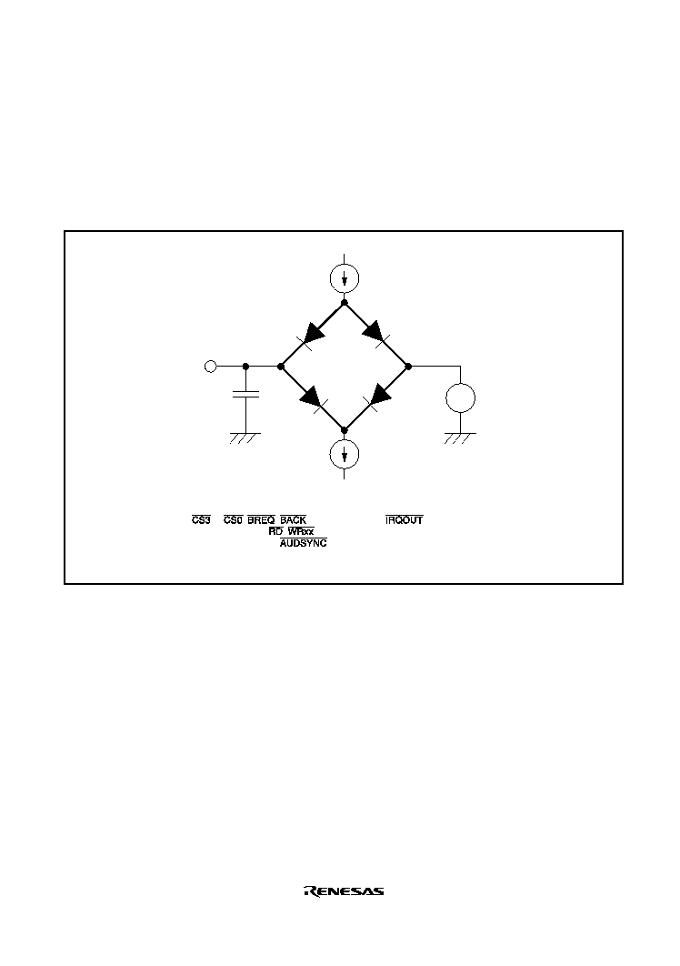
Rev. 2.0, 09/02, page 669 of 732
26.3
AC Characteristics
26.3.1
Test conditions for the AC characteristics
Input reference levels
high level: V
IH
minimum value, low level: V
IL
maximum value
Output reference levels
high level: 2.0 V, low level: 0.8 V
I
OL
I
OH
C
L
V
REF
V
DUT output
LSI output pin
CL is a total value that includes the capacitance of measurement equipment, and is set as follows:
30 pF: CK,
to
,
,
, DACK1, DACK0,
, AUDCK
50 pF: A21 to A0, D31 to D0,
,
, TDO
100 pF: AUDATA3 to AUDATA0,
70 pF: Port output pin other than the above and peripheral module output pins
It is assumed that I
OL
= 1.6 mA, I
OH
= 200
µ
A in the test conditions.
Figure 26.1 Output Load Circuit
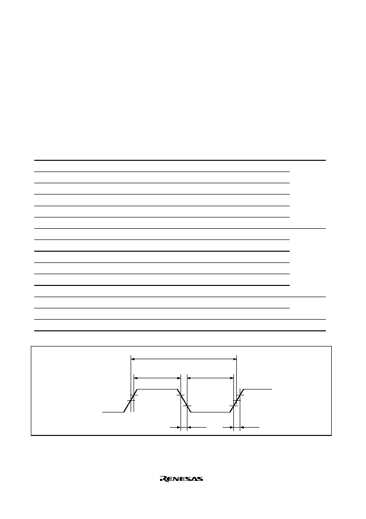
Rev. 2.0, 09/02, page 670 of 732
26.3.2
Clock timing
Table 26.4 shows the clock timing.
Table 26.4 Clock Timing
Conditions: V
CC
= PLLV
CC
=3.3 V ± 0.3 V, AV
CC
= 3.3 V ± 0.3 V, AV
CC
= V
CC
± 0.3 V,
AV
ref
= 3.0 V to AV
CC
, V
SS
= PLLV
SS
= AV
SS
= 0 V, T
a
= ≠20
∞
C to +75
∞
C
(regular specifications), T
a
= ≠40
∞
C to +85
∞
C (wide-range specifications),
When programming or erasing flash memory, T
a
= ≠20
∞
C to +75
∞
C.
Item
Symbol
Min
Max
Unit
Figure
Operating frequency
f
op
4
50
MHz
Figure 26.2
Clock cycle time
t
cyc
20
250
ns
Clock low-level pulse width
t
CL
1/2 t
cyc
-
5
ns
Clock high-level pulse width
t
CH
1/2 t
cyc
-
5
ns
Clock rise time
t
CR
5
ns
Clock fall time
t
CF
5
ns
EXTAL clock input frequency
f
EX
4
12.5
MHz
Figure 26.3
EXTAL clock input cycle time
t
EXcyc
80
250
ns
EXTAL clock input low-level pulse width
t
EXL
35
ns
EXTAL clock input high-level pulse width
t
EXH
35
ns
EXTAL clock input rise time
t
EXR
5
ns
EXTAL clock input fall time
t
EXF
5
ns
Reset oscillation settling time
t
OSC1
10
ms
Figure 26.4
Standby return oscillation settling time
t
OSC2
10
ms
Clock cycle time for peripheral modules
t
pcyc
25
500
ns
t
cyc
t
CH
t
CF
t
CR
V
OH
CK
V
OH
1/2V
CC
1/2V
CC
V
OH
V
OL
V
OL
t
CL
Figure 26.2 System Clock Timing
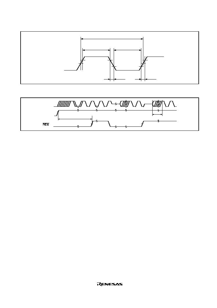
Rev. 2.0, 09/02, page 671 of 732
t
EXcyc
t
EXH
t
EXF
t
EXR
V
IH
EXTAL
V
IH
1/2V
CC
1/2V
CC
VIH
V
IL
V
IL
t
EXL
Figure 26.3 EXTAL Clock Input Timing
CK
V
CC
V
CC
min
t
osc1
t
osc2
Figure 26.4 Oscillation Settling Time

Rev. 2.0, 09/02, page 672 of 732
26.3.3
Control Signal Timing
Table 26.5 shows control signal timing.
Table 26.5 Control Signal Timing
Conditions: V
CC
= PLLV
CC
=3.3 V ± 0.3 V, AV
CC
= 3.3 V ± 0.3 V, AV
CC
= V
CC
± 0.3 V,
AV
ref
= 3.0 V to AV
CC
, V
SS
= PLLV
SS
= AV
SS
= 0 V, T
a
= ≠20
∞
C to +75
∞
C
(regular specifications), T
a
= ≠40
∞
C to +85
∞
C (wide-range specifications),
When programming or erasing flash memory, T
a
= ≠20
∞
C to +75
∞
C.
Item
Symbol
Min
Max
Unit
Figure
RES
rise time, fall time
t
RESr
, t
RESf
200
ns
Figure 26.5
RES
pulse width
t
RESW
25
t
cyc
RES
setup time
t
RESS
35
ns
MRES
pulse width
t
MRESW
20
t
cyc
MRES
setup time
t
MRESS
35
ns
MD3 to MD0 setup time
t
MDS
20
t
cyc
NMI rise time, fall time
t
NMIr
, t
NMIIf
200
ns
Figure 26.6
NMI setup time
t
NMIS
35
ns
NMI hold time
t
NMIH
35
ns
IRQ7
to
IRQ0
setup time
*
(edge detection)
t
IRQES
19
ns
IRQ7
to
IRQ0
setup time
*
(level detection)
t
IRQLS
19
ns
IRQ7
to
IRQ0
hold time
t
IRQEH
19
ns
IRQOUT
output delay time
t
IRQOD
100
ns
Figure 26.7
Bus request setup time
t
BRQS
19
ns
Figure 26.8
Bus acknowledge delay time 1
t
BACKD1
35
ns
Bus acknowledge delay time 2
t
BACKD2
35
ns
Bus three-state delay time
t
BZD
35
ns
[Operating Precautions]
Note: * The
RES, MRES, NMI and IRQ7 to IRQ0 signals are asynchronous inputs, but when the
setup times shown here are observed, the signals are considered to have been changed at
clock rise (
RES, MRES) or fall (NMI and IRQ7 to IRQ0). If the setup times are not
observed, the recognition of these signals may be delayed until the next clock rise or fall.
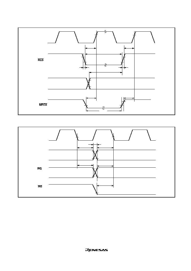
Rev. 2.0, 09/02, page 673 of 732
t
RESS
t
MDS
t
RESf
t
RESr
V
OH
V
IH
V
IH
V
IH
V
IL
V
IL
V
IL
t
RESS
t
RESW
CK
MD3 to
MD0
t
MRESW
t
MRESS
t
MRESS
V
IH
V
IL
V
IL
Figure 26.5 Reset Input Timing
V
IH
V
IH
V
IL
V
IL
t
NMIS
t
NMIr
t
NMIf
t
NMIH
V
IH
V
OL
V
OL
V
IL
V
IL
t
IRQES
t
IRQEH
t
IRQLS
CK
NMI
edge
level
Figure 26.6 Interrupt Signal Input Timing
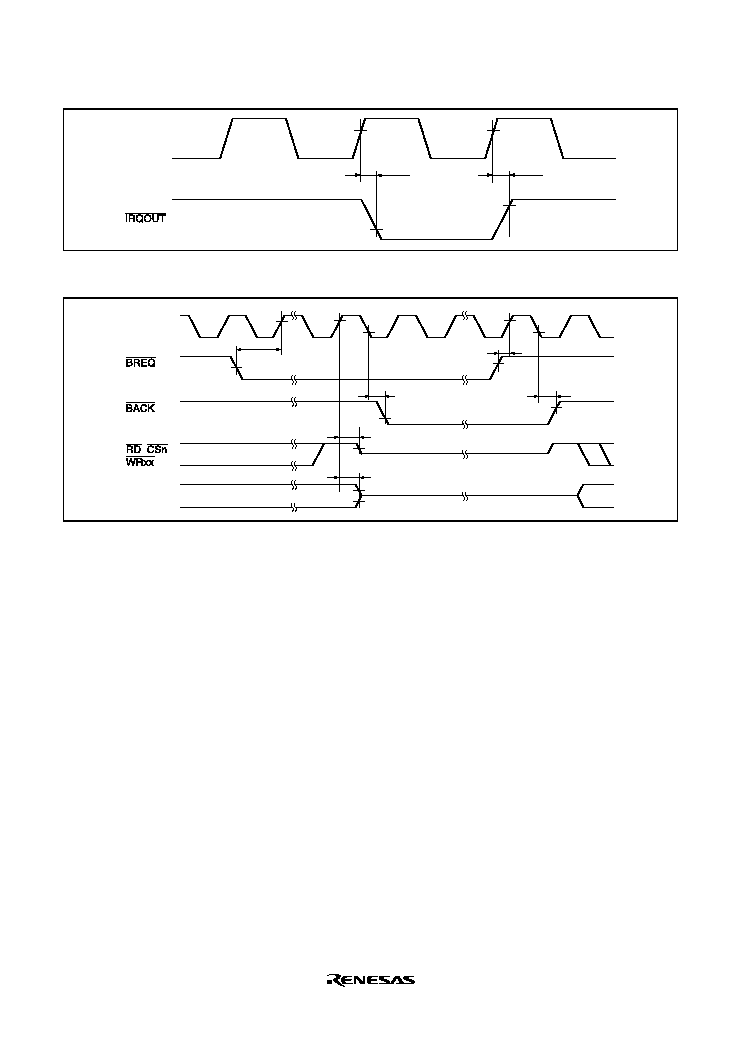
Rev. 2.0, 09/02, page 674 of 732
t
IRQOD
V
OH
V
OL
t
IRQOD
CK
V
OH
Figure 26.7 Interrupt Signal Output Timing
t
BRQS
t
BACKD1
t
BRQS
t
BZD
t
BZD
Hi-Z
Hi-Z
V
OL
V
OL
V
OL
V
OH
V
OH
V
OH
V
OH
V
IH
t
BACKD2
CK
(input)
(output)
,
,
A17 to A0,
D7 to D0
Figure 26.8 Bus Release Timing

Rev. 2.0, 09/02, page 675 of 732
26.3.4
Bus Timing
Table 26.6 shows bus timing.
Table 26.6 Bus Timing
Conditions: V
CC
= PLLV
CC
=3.3 V ± 0.3 V, AV
CC
= 3.3 V ± 0.3 V, AV
CC
= V
CC
± 0.3 V,
AV
ref
= 3.0 V to AV
CC
, V
SS
= PLLV
SS
= AV
SS
= 0 V, T
a
= ≠20
∞
C to +75
∞
C
(regular specifications), T
a
= ≠40
∞
C to +85
∞
C (wide-range specifications),
When programming or erasing flash memory, T
a
= ≠20
∞
C to +75
∞
C.
Item
Symbol
Min
Max
Unit
Figure
Address delay time
t
AD
25
ns
CS
delay time 1
t
CSD1
28
ns
CS
delay time 2
t
CSD2
28
ns
Read strobe delay time 1
t
RSD1
25
ns
Read strobe delay time 2
t
RSD2
25
ns
Read data setup time
t
RDS
15
ns
Read data hold time
t
RDH
0
ns
Write strobe delay time 1
t
WSD1
25
ns
Write strobe delay time 2
t
WSD2
25
ns
Write data delay time
t
WDD
30
ns
Write data hold time
t
WDH
0
ns
Figures 26.9,
26.10
WAIT
setup time
t
WTS
12
ns
WAIT
hold time
t
WTH
3
ns
Figure 26.11
Read data access time
t
ACC
t
cyc
◊
(n+2)
-
35
ns
Access time from read
strobe
t
OE
t
cyc
◊
(n+1.5)
-
33
ns
Address setup time (Write)
t
AS
0
ns
Address hold time (Write)
t
WR
5
ns
Write data hold time
t
WRH
0
ns
DACK delay time
t
DACKD
28
ns
Figures 26.9,
26.10
Note:
n = the number of waits
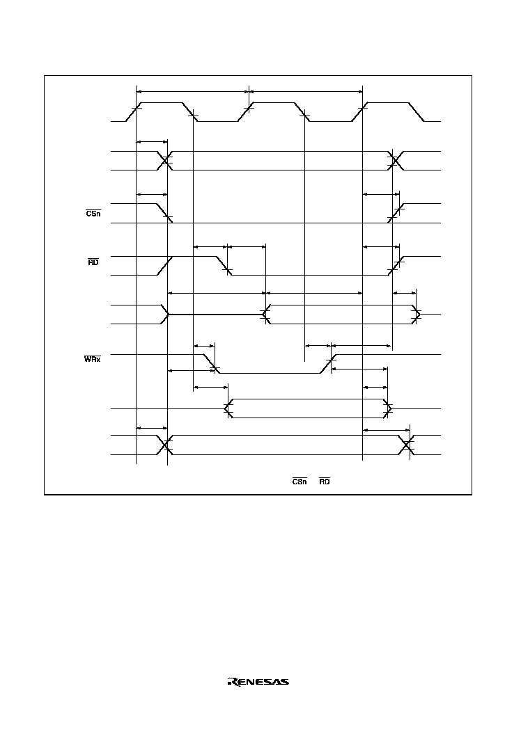
Rev. 2.0, 09/02, page 676 of 732
T
1
t
AD
V
OH
V
OL
T
2
t
DACKD
t
CSD1
t
RSD1
t
OE
t
RSD2
t
RDS
t
ACC
t
AS
t
RDH
t
WSD2
t
WR
t
WSD1
t
WRH
t
CSD2
t
WDH
t
DACKD
t
WDD
Note: t
RDH
is specified from the negate timing of A21 to A0,
, or
, whichever is first.
CK
DACKn
A21 to A0
(read)
(write)
D31 to D0
(read)
D31 to D0
(write)
Figure 26.9 Basic Cycle (No Waits)
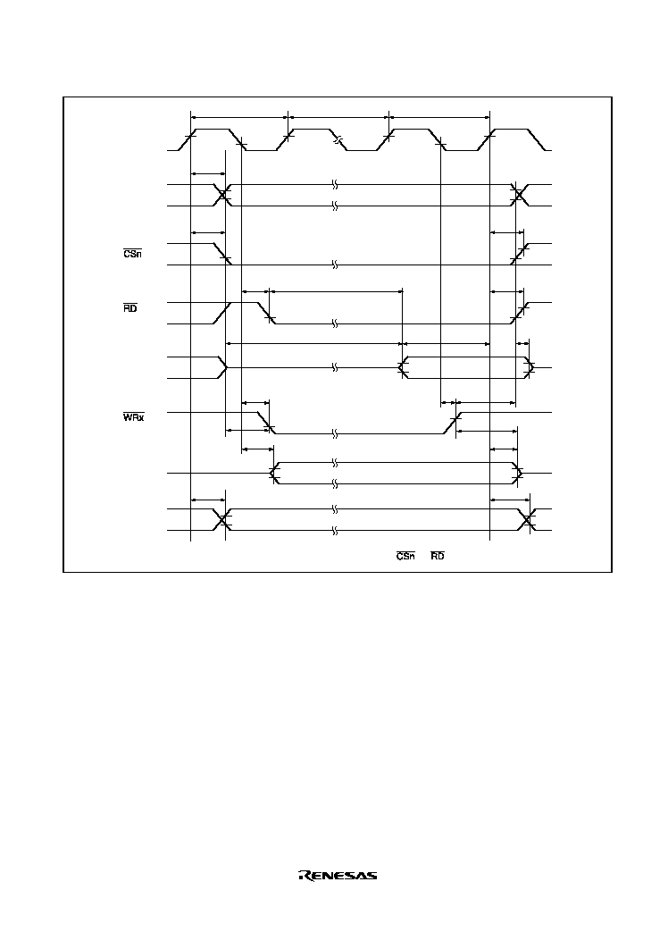
Rev. 2.0, 09/02, page 677 of 732
T1
t
AD
T
W
T
2
t
CSD1
V
OL
V
OH
t
RSD1
t
OE
t
RSD2
t
RDS
t
ACC
t
AS
t
RDH
t
WSD2
t
WR
t
WSD1
t
CSD2
t
WDH
t
DACKD
t
DACKD
t
WRH
t
WDD
Note: t
RDH
is specified from the negate timing of A21 to A0,
, or
, whichever is first.
CK
A21 to A0
(read)
(write)
D7 to D0
(read)
D7 to D0
(write)
DACKn
Figure 26.10 Basic Cycle (One Software Wait)
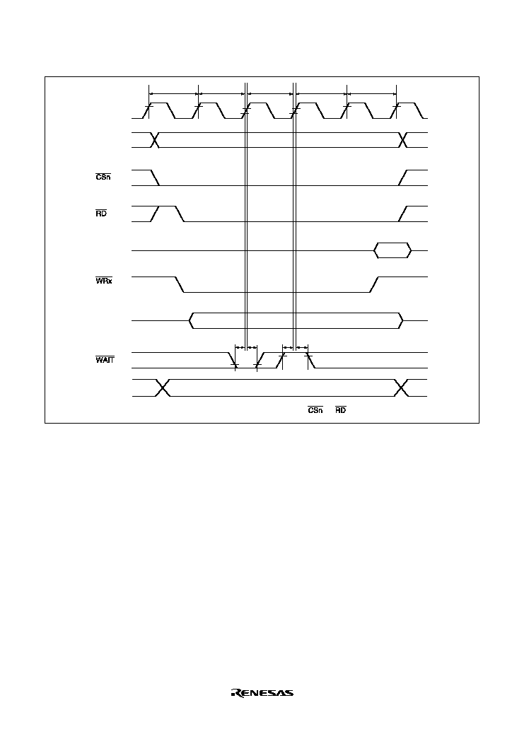
Rev. 2.0, 09/02, page 678 of 732
t
WTH
t
WTH
t
WTS
t
WTS
CK
A21 to A0
(read)
D7 to D0
(read)
D7 to D0
(write)
(write)
T1
TW
T
W
T
WO
T
2
Note: t
RDH
is specified from the negate timing of A21 to A0,
, or
, whichever is first.
DACKn
Figure 26.11 Basic Cycle (Two Software Waits + Waits by WAIT Signal)
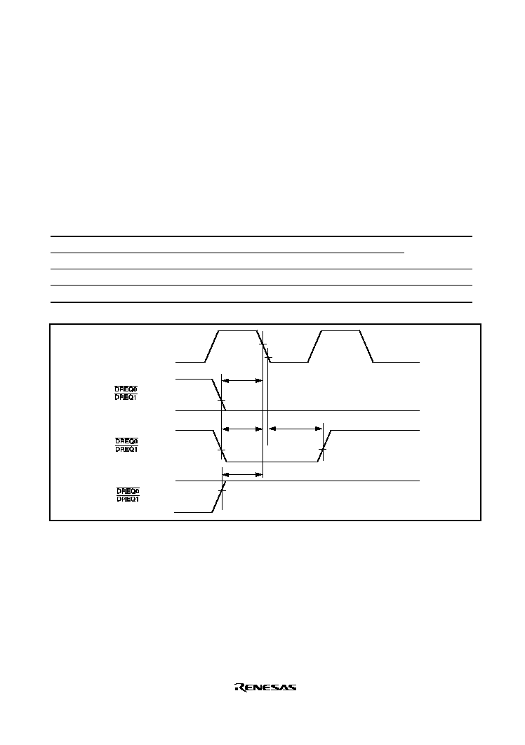
Rev. 2.0, 09/02, page 679 of 732
26.3.5
Direct Memory Access Controller (DMAC) Timing
Table 26.7 shows direct memory access controller timing.
Table 26.7 Direct Memory Access Controller Timing
Conditions: V
CC
= PLLV
CC
=3.3 V ± 0.3 V, AV
CC
= 3.3 V ± 0.3 V, AV
CC
= V
CC
± 0.3 V,
AV
ref
= 3.0 V to AV
CC
, V
SS
= PLLV
SS
= AV
SS
= 0 V, T
a
= ≠20
∞
C to +75
∞
C
(regular specifications), T
a
= ≠40
∞
C to +85
∞
C (wide-range specifications),
When programming or erasing flash memory, T
a
= ≠20
∞
C to +75
∞
C.
Item
Symbol
Min
Max
Unit
Figure
DREQ0
,
DREQ1
setup time
t
DRQS
10
ns
Figure 26.12
DREQ0
,
DREQ1
hold time
t
DRQH
1.5 t
cyc
-
10
ns
DREQ0
,
DREQ1
pulse width
t
DRQW
1.5
t
cyc
Figure 26.13
DRAK0, DRAK1 output delay time
t
DRAKD
30
ns
Figure 26.14
CK
level input
edge input
level cancel
t
DRQS
t
DRQS
t
DRQS
t
DRQH
Figure 26.12
DREQ0
DREQ0
DREQ0
DREQ0, DREQ1
DREQ1
DREQ1
DREQ1 Input Timing (1)
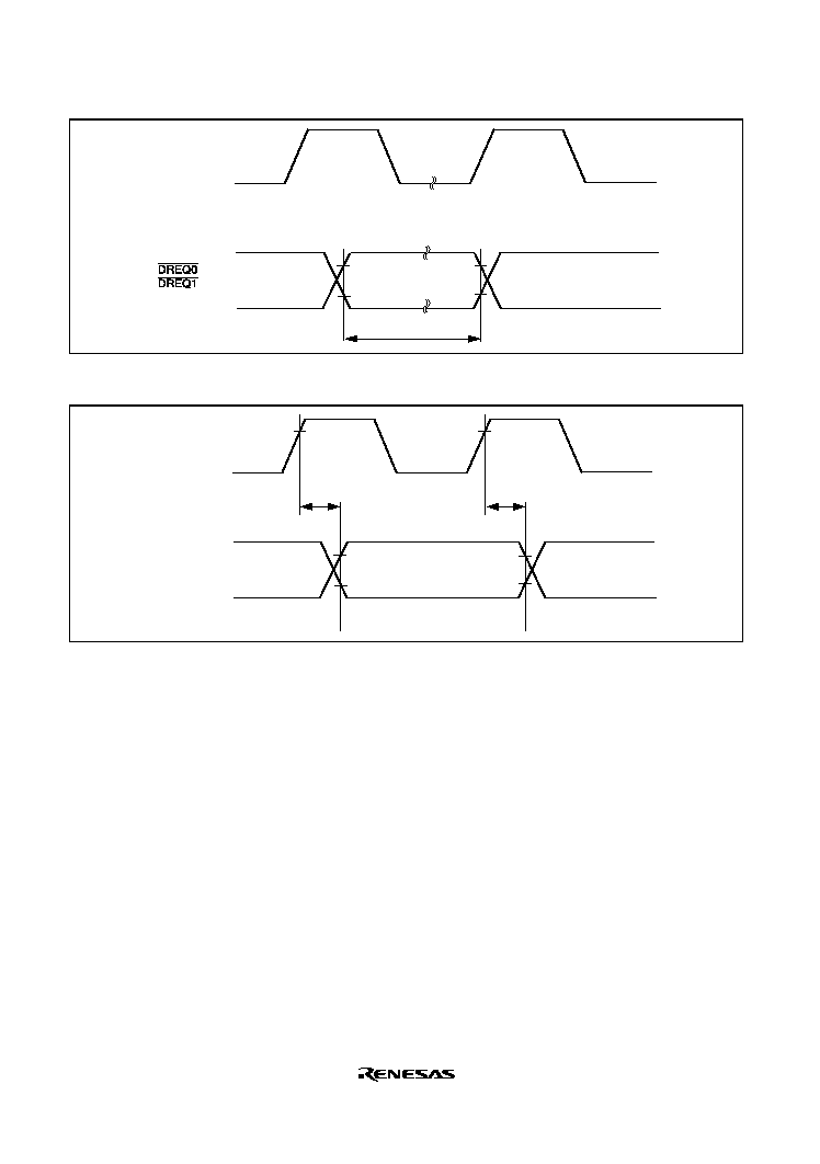
Rev. 2.0, 09/02, page 680 of 732
CK
edge input
t
DRQW
Figure 26.13
DREQ0
DREQ0
DREQ0
DREQ0, DREQ1
DREQ1
DREQ1
DREQ1 Input Timing (2)
CK
DRAK0
DRAK1
output
t
DRAKD
t
DRAKD
Figure 26.14 DRAK Output Delay Time
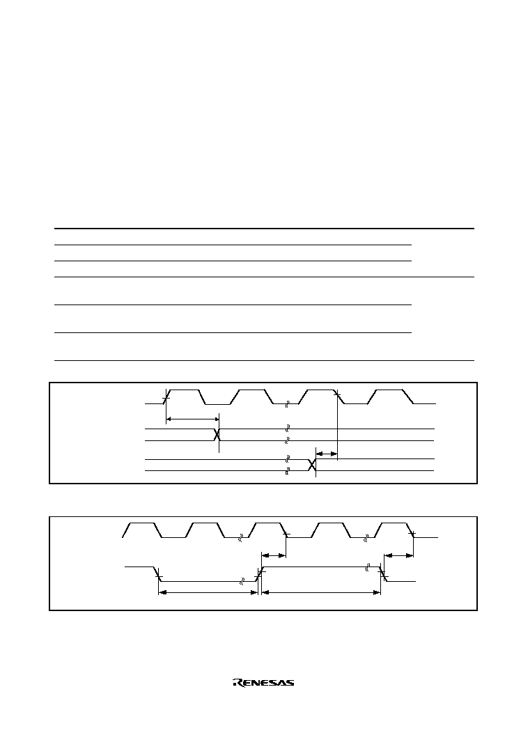
Rev. 2.0, 09/02, page 681 of 732
26.3.6
Multi-Function Timer Pulse Unit (MTU)Timing
Table 26.8 shows Multi-Function timer pulse unit timing.
Table 26.8 Multi-Function Timer Pulse Unit Timing
Conditions: V
CC
= PLLV
CC
=3.3 V ± 0.3 V, AV
CC
= 3.3 V ± 0.3 V, AV
CC
= V
CC
± 0.3 V,
AV
ref
= 3.0 V to AV
CC
, V
SS
= PLLV
SS
= AV
SS
= 0 V, T
a
= ≠20
∞
C to +75
∞
C
(regular specifications), T
a
= ≠40
∞
C to +85
∞
C (wide-range specifications),
When programming or erasing flash memory, T
a
= ≠20
∞
C to +75
∞
C.
Item
Symbol
Min
Max
Unit
Figure
Output compare output delay time
t
TOCD
100
ns
Figure 26.15
Input capture input setup time
t
TICS
19
ns
Timer input setup time
t
TCKS
19
ns
Timer clock pulse width (single edge
specified)
t
TCKWH/L
1.5
t
pcyc
Figure 26.16
Timer clock pulse width (both edges
specified)
t
TCKWH/L
2.5
t
pcyc
Timer clock pulse width (phase count
mode)
t
TCKWH/L
2.5
t
pcyc
CK
Output compare
output
Input capture
input
t
TOCD
t
TICS
Figure 26.15 MTU Input/Output timing
CK
TCLKA to
TCLKD
t
TCKS
t
TCKS
t
TCKWH
t
TCKWL
Figure 26.16 MTU Clock Input Timing
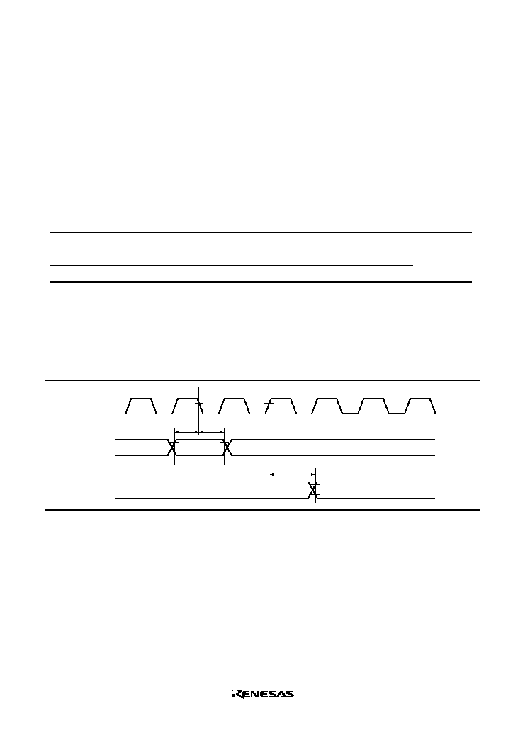
Rev. 2.0, 09/02, page 682 of 732
26.3.7
I/O Port Timing
Table 26.9 shows I/O port timing.
Table 26.9 I/O Port Timing
Conditions: V
CC
= PLLV
CC
=3.3 V ± 0.3 V, AV
CC
= 3.3 V ± 0.3 V, AV
CC
= V
CC
± 0.3 V,
AV
ref
= 3.0 V to AV
CC
, V
SS
= PLLV
SS
= AV
SS
= 0 V, T
a
= ≠20
∞
C to +75
∞
C
(regular specifications), T
a
= ≠40
∞
C to +85
∞
C (wide-range specifications),
When programming or erasing flash memory, T
a
= ≠20
∞
C to +75
∞
C.
Item
Symbol
Min
Max
Unit
Figure
Port output data delay time
t
PWD
100
ns
Figure 26.17
Port input hold time
t
PRH
19
ns
Port input setup time
t
PRS
19
ns
[Operating precautions]
The port input signals are asynchronous. They are, however, considered to have been changed at
CK clock fall with two-state intervals shown in figure 26.17. If the setup times shown here are not
observed, recognition may be delayed until the clock fall two states after that timing.
t
PRS
t
PRH
t
PWD
CK
Port
(read)
Port
(write)
Figure 26.17 I/O Port Input/Output timing
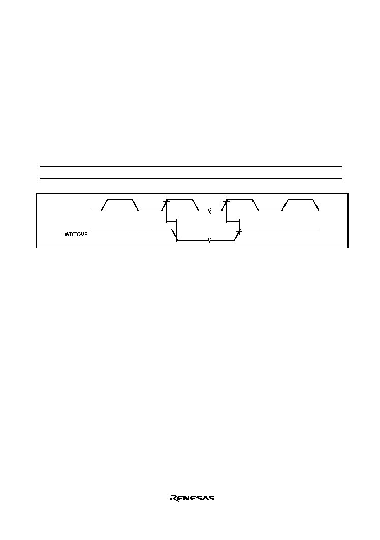
Rev. 2.0, 09/02, page 683 of 732
26.3.8
Watchdog Timer (WDT)Timing
Table 26.10 shows watchdog timer timing.
Table 26.10 Watchdog Timer Timing
Conditions: V
CC
= PLLV
CC
=3.3 V ± 0.3 V, AV
CC
= 3.3 V ± 0.3 V, AV
CC
= V
CC
± 0.3 V,
AV
ref
= 3.0 V to AV
CC
, V
SS
= PLLV
SS
= AV
SS
= 0 V, T
a
= ≠20
∞
C to +75
∞
C
(regular specifications), T
a
= ≠40
∞
C to +85
∞
C (wide-range specifications),
When programming or erasing flash memory, T
a
= ≠20
∞
C to +75
∞
C.
Item
Symbol
Min
Max
Unit
Figure
WDTOVF
delay time
t
WOVD
--
100
ns
Figure 26.18
t
WOVD
t
WOVD
V
OH
V
OH
CK
Figure 26.18 WDT Timing
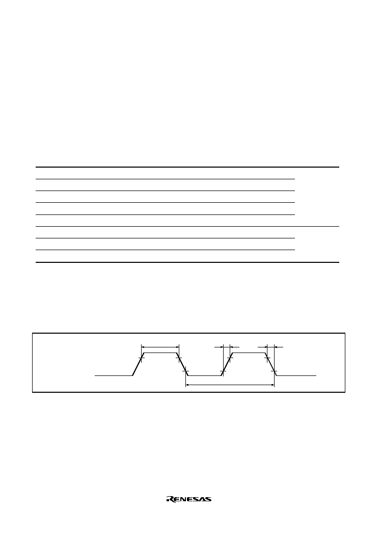
Rev. 2.0, 09/02, page 684 of 732
26.3.9
Serial Communication Interface (SCI)Timing
Table 26.11 shows serial communication interface timing.
Table 26.11 Serial Communication Interface Timing
Conditions: V
CC
= PLLV
CC
=3.3 V ± 0.3 V, AV
CC
= 3.3 V ± 0.3 V, AV
CC
= V
CC
± 0.3 V,
AV
ref
= 3.0 V to AV
CC
, V
SS
= PLLV
SS
= AV
SS
= 0 V, T
a
= ≠20
∞
C to +75
∞
C
(regular specifications), T
a
= ≠40
∞
C to +85
∞
C (wide-range specifications),
When programming or erasing flash memory, T
a
= ≠20
∞
C to +75
∞
C.
Item
Symbol
Min
Max
Unit
Figure
Input clock cycle
t
scyc
4
t
pcyc
Figure 26.19
Input clock cycle (clock sync)
t
scyc
6
t
pcyc
Input clock pulse width
t
sckw
0.4
0.6
t
scyc
Input clock rise time
t
sckr
1.5
t
pcyc
Input clock fall time
t
sckf
1.5
t
pcyc
Transmit data delay time
t
TxD
100
ns
Figure 26.20
Received data setup time
t
RxS
100
ns
Received data hold time
t
RxH
100
ns
[Operating Precautions]
The inputs and outputs are asynchronous in asynchronous mode, but as shown in figure 26.19, the
received data is considered to have been changed at CK clock rise (two-clock intervals). The
transmit signals change with a reference of CK clock rise (two-clock intervals).
t
sckw
V
IH
V
IH
V
IH
V
IH
V
IL
V
IL
V
IL
SCK0 to SCK3
t
sckr
t
sckf
t
scyc
Figure 26.19 SCI Input Timing
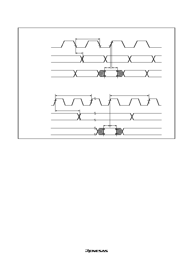
Rev. 2.0, 09/02, page 685 of 732
t
scyc
SCK0 to SCK3
(input/output)
TxD0 to TxD3
(transmit data)
RxD0 to RxD3
(received data)
SCI input/output timing (clock synchronous mode)
t
TxD
t
RxS
t
RxH
V
OH
V
OH
T
1
CK
TxD0 to TxD3
(transmit data)
RxD0 to RxD3
(received data)
SCI input/output timing (asynchronous mode)
T
n
t
TxD
t
RxS
t
RxH
Figure 26.20 SCI Input/Output Timing

Rev. 2.0, 09/02, page 686 of 732
26.3.10
I
2
C Bus Interface Timing
Table 26.12 shows I
2
C bus interface timing.
Table 26.12 I
2
C Bus Interface Timing
Conditions: V
CC
= PLLV
CC
=3.3 V ± 0.3 V, AV
CC
= 3.3 V ± 0.3 V, AV
CC
= V
CC
± 0.3 V,
AV
ref
= 3.0 V to AV
CC
, V
SS
= PLLV
SS
= AV
SS
= 0 V, T
a
= ≠20
∞
C to +75
∞
C
(regular specifications), T
a
= ≠40
∞
C to +85
∞
C (wide-range specifications),
When programming or erasing flash memory, T
a
= ≠20
∞
C to +75
∞
C.
Item
Symbol
Min
Typ
Max
Unit
Figure
SCL input cycle time
t
SCL
12 t
pcyc
*
1
ns
SCL input high pulse width
t
SCLH
3 t
pcyc
ns
SCL input low pulse width
t
SCLL
5 t
pcyc
ns
SCL and SDA input rise time
t
Sr
7.5 t
pcyc
*
2
ns
SCL and SDA input fall time
t
Sf
300
ns
SCL and SDA input spike
pulse removal time
t
SP
1 t
pcyc
ns
SDA input bus free time
t
BUF
5 t
pcyc
ns
Start condition input hold
time
t
STAH
3 t
pcyc
ns
Retransmission start
condition input setup time
t
STAS
3 t
pcyc
ns
Halt condition input setup
time
t
STOS
3 t
pcyc
ns
Data input setup time
t
SDAS
35
ns
Data input hold time
t
SDAH
0
ns
Figure 26.21
SCL and SDA capacity load
C
b
400
pF
Notes: 1. t
pcyc
(ns) = 1/(P
supplied to I
2
C module (MHz) )
2. Can be set to 17.5 t
pcyc
by selecting the clock to be used for the I
2
C module. For details,
refer to section 14.5, Usage Notes.
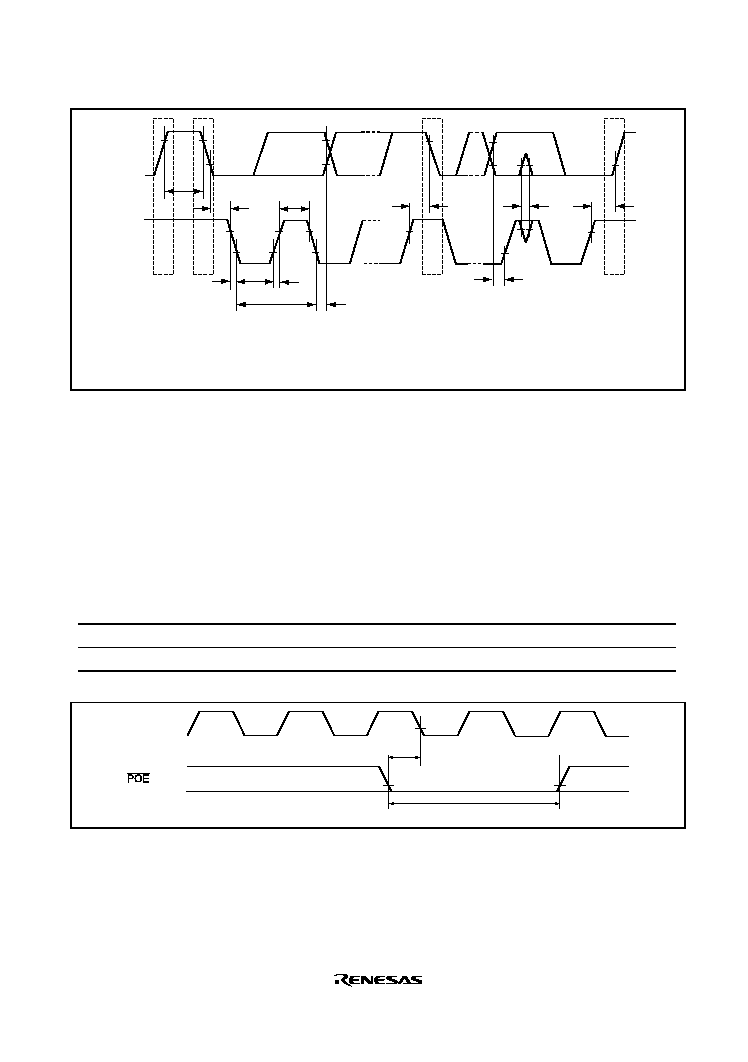
Rev. 2.0, 09/02, page 687 of 732
SCL0
V
IH
V
IL
t
STAH
t
BUF
P
*
S
*
t
Sf
t
Sr
t
SCL
t
SDAH
t
SCLH
t
SCLL
SDA0
Sr
*
t
STAS
t
SP
t
STOS
t
SDAS
P
*
Note:
*
S, P, and Sr represent the following conditions
S: Start
P: Halt
Sr: Retransmission start
Figure 26.21 I
2
C Bus Interface Timing
26.3.11
Output Enable (POE) Timing
Table 26.13 Output Enable Timing
Conditions: V
CC
= PLLV
CC
=3.3 V ± 0.3 V, AV
CC
= 3.3 V ± 0.3 V, AV
CC
= V
CC
± 0.3 V,
AV
ref
= 3.0 V to AV
CC
, V
SS
= PLLV
SS
= AV
SS
= 0 V, T
a
= ≠20
∞
C to +75
∞
C
(regular specifications), T
a
= ≠40
∞
C to +85
∞
C (wide-range specifications),
When programming or erasing flash memory, T
a
= ≠20
∞
C to +75
∞
C.
Item
Symbol
Min
Max
Unit
Figure
POE
input setup time
t
POES
100
--
ns
Figure 26.22
POE
input pulse width
t
POEW
1.5
--
tpcyc
CK
input
t
POES
t
POEW
Figure 26.22
POE
POE
POE
POE Input/Output Timing
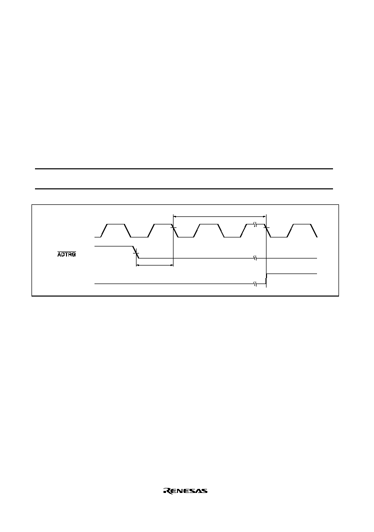
Rev. 2.0, 09/02, page 688 of 732
26.3.12
A/D Converter Timing
Table 26.14 shows A/D converter timing.
Table 26.14 A/D Converter Timing
Conditions: V
CC
= PLLV
CC
=3.3 V ± 0.3 V, AV
CC
= 3.3 V ± 0.3 V, AV
CC
= V
CC
± 0.3 V,
AV
ref
= 3.0 V to AV
CC
, V
SS
= PLLV
SS
= AV
SS
= 0 V, T
a
= ≠20
∞
C to +75
∞
C
(regular specifications), T
a
= ≠40
∞
C to +85
∞
C (wide-range specifications),
When programming or erasing flash memory, T
a
= ≠20
∞
C to +75
∞
C.
Item
Symbol
Min
Typ
Max
Unit
Figure
External trigger input start
delay time
t
TRGS
50
--
--
ns
Figure 26.23
CK
input
ADCRn Register
(ADST = 1 set)
3≠5 states
t
TRGS
V
OH
Figure 26.23 External Trigger Input Timing
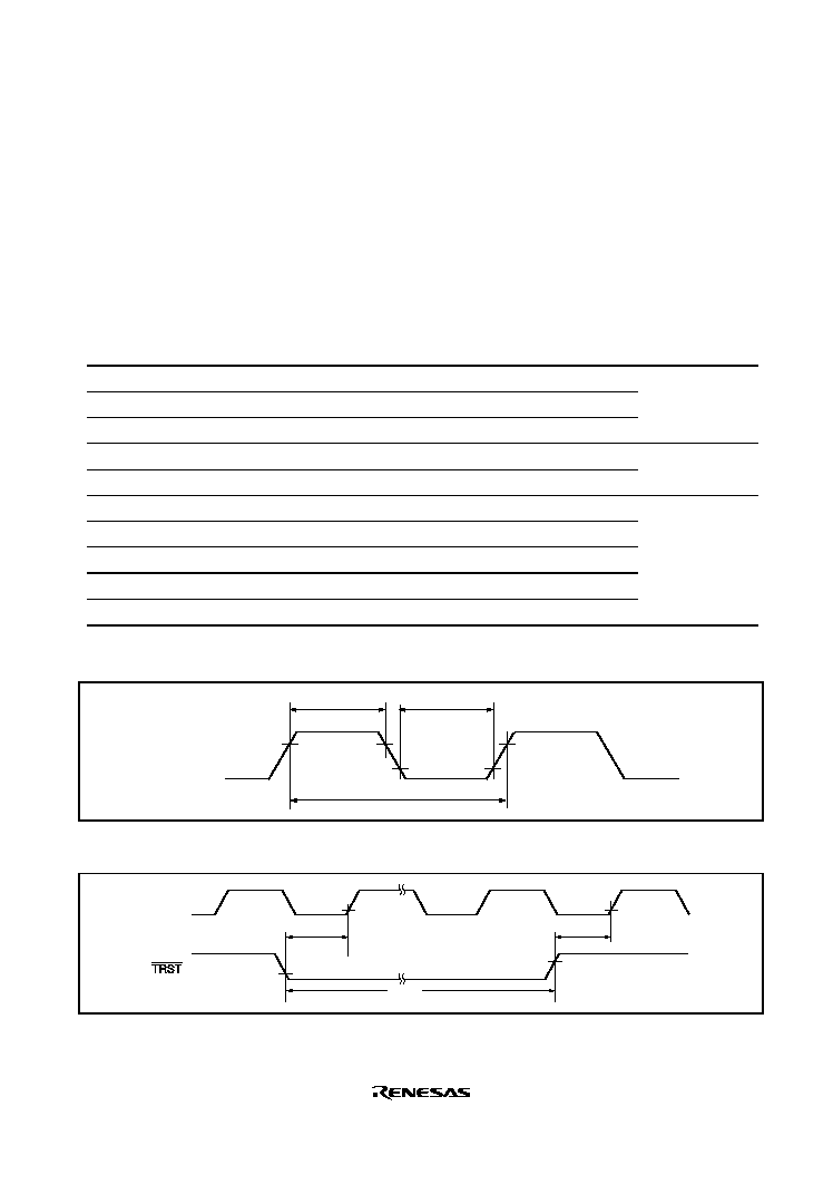
Rev. 2.0, 09/02, page 689 of 732
26.3.13
H-UDI Timing
Table 26.15 shows H-UDI timing.
Table 26.15 H-UDI Timing
Conditions: V
CC
= PLLV
CC
=3.3 V ± 0.3 V, AV
CC
= 3.3 V ± 0.3 V, AV
CC
= V
CC
± 0.3 V,
AV
ref
= 3.0 V to AV
CC
, V
SS
= PLLV
SS
= AV
SS
= 0 V, T
a
= ≠20
∞
C to +75
∞
C
(regular specifications), T
a
= ≠40
∞
C to +85
∞
C (wide-range specifications),
When programming or erasing flash memory, T
a
= ≠20
∞
C to +75
∞
C.
Item
Symbol
Min
Max
Unit
Figure
TCK clock cycle
t
tcyc
60
*
ns
Figure 26.24
TCK clock high-level width
t
TCKH
0.4
0.6
t
tcyc
TCK clock low-level width
t
TCKL
0.4
0.6
t
tcyc
TRST
pulse width
t
TRSW
20
t
tcyc
Figure 26.25
TRST
setup time
t
TRSS
30
ns
TMS setup time
t
TMSS
15
ns
Figure 26.26
TMS hold time
t
TMSH
10
ns
TDI setup time
t
TDIS
15
ns
TDI hold time
t
TDIH
10
ns
TDO delay time
t
TDOD
30
ns
Note:
*
The value must not be under 2
◊
t
cyc
.
t
TCKH
t
tcyc
V
IH
TCK
V
IH
V
IL
V
IL
V
IH
t
TCKL
Figure 26.24 H-UDI Clock Timing
t
TRSS
t
TRSS
V
IL
V
IL
V
IH
V
IL
TCK
t
TRSW
Figure 26.25 H-UDI
TRST
TRST
TRST
TRST Timing
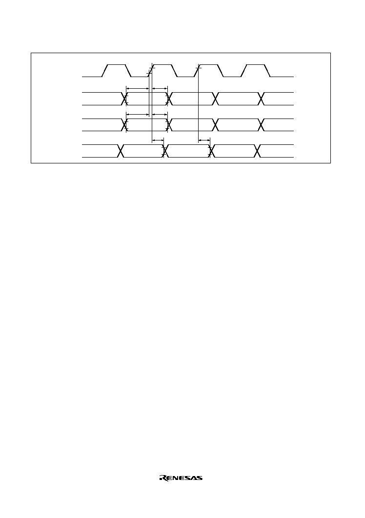
Rev. 2.0, 09/02, page 690 of 732
TCK
TMS
TDI
TDO
t
TMSS
t
TMSH
V
IL
V
IH
V
IH
t
TDIS
t
TDIH
t
TDOD
t
TDOD
Figure 26.26 H-UDI Input/Output Timing

Rev. 2.0, 09/02, page 691 of 732
26.3.14
AUD Timing
Table 26.16 shows AUD timing.
Table 26.16 AUD Timing
Conditions: V
CC
= PLLV
CC
=3.3 V ± 0.3 V, AV
CC
= 3.3 V ± 0.3 V, AV
CC
= V
CC
± 0.3 V,
AV
ref
= 3.0 V to AV
CC
, V
SS
= PLLV
SS
= AV
SS
= 0 V, T
a
= ≠20
∞
C to +75
∞
C
(regular specifications), T
a
= ≠40
∞
C to +85
∞
C (wide-range specifications),
When programming or erasing flash memory, T
a
= ≠20
∞
C to +75
∞
C.
Item
Symbol
Min
Max
Unit
Figure
AUDRST
pulse width (Branch trace)
t
AUDRSTW
20
t
cyc
Figure 26.27
AUDRST
pulse width (RAM monitor)
t
AUDRSTW
5
t
RMCYC
AUDMD setup time (Branch trace)
t
AUDMDS
20
t
cyc
AUDMD setup time (RAM monitor)
t
AUDMDS
5
t
RMCYC
Branch trace clock cycle
t
BTCYC
2
2
t
cyc
Figure 26.28
Branch trace clock duty
t
BTCKW
40
60
%
Branch trace data delay time
t
BTDD
11
ns
Branch trace data hold time
t
BTDH
-
10
ns
Branch trace SYNC delay time
t
BTSD
10
ns
Branch trace SYNC hold time
t
BTSH
-
10
ns
RAM monitor clock cycle
t
RMCYC
80
ns
Figure 26.29
RAM monitor clock low pulse width
t
RMCKW
35
ns
RAM monitor output data delay time
t
RMDD
7
t
RMCYC
-
20
ns
RAM monitor output data hold time
t
RMDHD
5
ns
RAM monitor input data setup time
t
RMDS
10
ns
RAM monitor input data hold time
t
RMDH
15
ns
RAM monitor SYNC setup time
t
RMSS
10
ns
RAM monitor SYNC hold time
t
RMSH
13
ns
Load conditions: AUDCK (output):
CL = 30 pF
AUDSYNC
:
CL = 100 pF
AUDATA3 to AUDATA0: CL = 100 pF
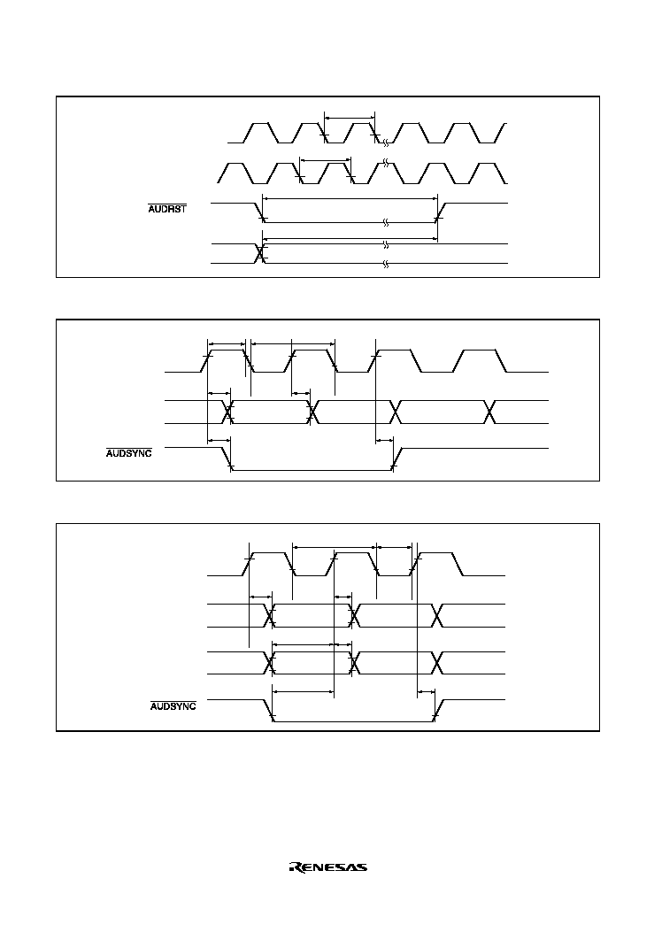
Rev. 2.0, 09/02, page 692 of 732
t
RMCYC
t
AUDRSTW
t
AUDMDS
t
cyc
CK
(Branch trace)
AUDCK (input)
(RAM monitor)
AUDMD
Figure 26.27 AUD Reset Timing
AUDCK
(output)
AUDATA3 to
AUDATA0
(output)
(output)
t
BTDD
t
BTSD
t
BTCKW
t
BTCYC
t
BTDH
t
BTSH
Figure 26.28 Branch Trace Timing
AUDCK
(input)
AUDATA3 to
AUDATA0
(output)
AUDATA3 to
AUDATA0
(input)
(input)
t
RMDD
t
RMDS
t
RMSS
t
RMDH
t
RMCYC
t
RMCKW
t
RMDHD
t
RMSH
Figure 26.29 RAM Monitor Timing

Rev. 2.0, 09/02, page 693 of 732
26.4
A/D Converter Characteristics
Table 26.17 shows A/D converter characteristics.
Table 26.17 A/D Converter Characteristics
Conditions: V
CC
= PLLV
CC
=3.3 V ± 0.3 V, AV
CC
= 3.3 V ± 0.3 V, AV
CC
= V
CC
± 0.3 V,
AV
ref
= 3.0 V to AV
CC
, V
SS
= PLLV
SS
= AV
SS
= 0 V, T
a
= ≠20
∞
C to +75
∞
C
(regular specifications), T
a
= ≠40
∞
C to +85
∞
C (wide-range specifications),
When programming or erasing flash memory, T
a
= ≠20
∞
C to +75
∞
C.
Item
Min
Typ
Max
Unit
Resolution
10
10
10
bit
A/D conversion time
--
--
6.7
*
1
/5.4
*
2
µ
s
Analog input capacitance
--
--
20
pF
Permitted analog signal source impedance
--
--
1
k
Non-linear error
--
--
±
3.0
*
3
*
4
*
5
/
±
5.0
*
6
LSB
Offset error
--
--
±
3.0
*
3
*
4
*
5
/
±
5.0
*
6
LSB
Full-scale error
--
--
±
3.0
*
3
*
4
*
5
/
±
5.0
*
6
LSB
Quantization error
--
--
±
0.5
LSB
Absolute error
--
--
±
4.0
*
3
*
4
*
5
/
±
6.0
*
6
LSB
Notes: 1. This is a value when (CKS1, 0) = (1,1) and t
pcyc
= 50 ns.
2. This is a value when (CKS1, 0) = (1,1) and t
pcyc
= 40 ns.
3. This is a value when (CKS1, 0) = (1,1), t
pcyc
= 50 ns, and T
a
=
-
20 to
+
75
∞
C (regular
specifications).
4. This is a value when (CKS1, 0) = (1,1), t
pcyc
= 40 ns, and T
a
=
-
20 to
+
75
∞
C (regular
specifications).
5. This is a value when (CKS1, 0) = (1,1), t
pcyc
= 50 ns, and T
a
=
-
40 to
+
85
∞
C (wide-range
specifications).
6. This is a value when (CKS1, 0) = (1,1), t
pcyc
= 40 ns, and T
a
=
-
40 to
+
85
∞
C (wide-range
specifications).

Rev. 2.0, 09/02, page 694 of 732
26.5
Flash Memory Characteristics
Table 26.18 shows flash memory characteristics.
Table 26.18 Flash Memory Characteristics
Conditions: V
CC
= PLLV
CC
=3.3 V ± 0.3 V, AV
CC
= 3.3 V ± 0.3 V, AV
CC
= V
CC
± 0.3 V,
AV
ref
= 3.0 V to AV
CC
, V
SS
= PLLV
SS
= AV
SS
= 0 V, T
a
= ≠20
∞
C to +75
∞
C
(regular specifications), T
a
= ≠40
∞
C to +85
∞
C (wide-range specifications),
When programming or erasing flash memory, T
a
= ≠20
∞
C to +75
∞
C.
Item
Symbol
Min
Typ
Max Unit
Remarks
Programming time
*
1,
*
2,
*
4
t
P
--
10
200
ms/
128 bytes
Erase time
*
1,
*
3,
*
5
t
E
--
100
1200 ms/block
Reprogramming count
N
WEC
100
6
10000
7
--
Times
Programming
Wait time after SWE bit setting
*
1
t
sswe
1
1
--
µs
Wait time after PSU bit setting
*
1
t
spsu
50
50
--
µs
Wait time after P bit setting
*
1,
*
4
t
sp30
28
30
32
µs
Programming
time wait
t
sp200
198
200
202
µs
Programming
time wait
t
sp10
8
10
12
µs
Additional-
programming
time wait
Wait time after P bit clear
*
1
t
cp
5
5
--
µs
Wait time after PSU bit clear
*
1
t
cpsu
5
5
--
µs
Wait time after PV bit setting
*
1
t
spv
4
4
--
µs
Wait time after H'FF dummy write
*
1
t
spvr
2
2
--
µs
Wait time after PV bit clear
*
1
t
cpv
2
2
--
µs
Wait time after SWE bit clear
*
1
t
cswe
100
100
--
µs
Maximum programming count
*
1,
*
4
N
--
--
1000 Times

Rev. 2.0, 09/02, page 695 of 732
Item
Symbol
Min
Typ
Max
Unit
Remarks
Erase
Wait time after SWE bit setting
*
1
t
sswe
1
1
--
µs
Wait time after ESU bit setting
*
1
t
sesu
100
100
--
µs
Wait time after E bit setting
*
1,
*
5
t
se
10
10
100
ms
Erase time
wait
Wait time after E bit clear
*
1
t
ce
10
10
--
µs
Wait time after ESU bit clear
*
1
t
cesu
10
10
--
µs
Wait time after EV bit setting
*
1
t
sev
20
20
--
µs
Wait time after H'FF dummy write
*
1
t
sevr
2
2
--
µs
Wait time after EV bit clear
*
1
t
cev
4
4
--
µs
Wait time after SWE bit clear
*
1
t
cswe
100
100
--
µs
Maximum erase count
*
1,
*
5
N
12
--
120
Times
Notes: 1. Make each time setting in accordance with the program/program-verify algorithm or
erase/erase-verify algorithm.
2. Programming time per 128 bytes (shows the total period for which the P-bit in the flash
memory control register (FLMCR1) is set. It does not include the programming
verification time.)
3. 1-Block erase time (shows the total period for which the E-bit in FLMCR1 is set. It does
not include the erase verification time.)
4. To specify the maximum programming time value (tp (max)) in the 128-bytes
programming algorithm, set the max. value (1000) for the maximum programming count
(N).
The wait time after P bit setting should be changed as follows according to the value of
the programming counter (n).
Programming counter (n) = 1 to 6:
t
sp30
= 30
µ
s
Programming counter (n) = 7 to 1000: t
sp200
= 200
µ
s
[In additional programming]
Programming counter (n) = 1 to 6:
t
sp10
= 10
µ
s
5. For the maximum erase time (t
E
(max)), the following relationship applies between the
wait time after E bit setting (t
se
) and the maximum erase count (N):
t
E
(max) = Wait time after E bit setting (t
se
) x maximum erase count (N)
To set the maximum erase time, the values of (t
se
) and (N) should be set so as to satisfy
the above formula.
Examples: When t
se
= 100 ms, N = 12 times
When t
se
= 10 ms, N = 120 times
6. The minimum times that all characteristics after rewriting are guaranteed. (A range
between 1 and minimum value is guaranteed.)
7. The reference value at 25∞C. (Normally, it is a reference that rewriting is enabled up to
this value.)

Rev. 2.0, 09/02, page 696 of 732

Rev. 2.0, 09/02, page 697 of 732
Appendix A Pin States
A.
Pin State
Pin initial states differ according to MCU operating modes. Refer to section 17, Pin Function
Controller (PFC), for details.
Table A.1 Pin States (SH7144)
Pin Function
Pin State
Reset State
Power-Down State
Power-On
Expansion
without
ROM
Type
Pin Name
8
bits
16
bits
Expansion
with ROM
Single
-chip
Manual
Software
Standby
Sleep
Bus
Master-
ship
Release
Software
Standby
in Bus
Master-
ship
Release
CK
O
O
O
Z
O
H
*
1
O
O
O
XTAL
O
O
O
O
O
L
O
O
L
EXTAL
I
I
I
I
I
I
I
I
I
Clock
PLLCAP
I
I
I
I
I
I
I
I
I
RES
I
I
I
I
I
I
I
I
I
MRES
Z
Z
Z
Z
I
Z
I
I
Z
WDTOVF
O
*
2
O
*
2
O
*
2
O
*
2
O
O
O
O
O
BREQ
Z
Z
Z
Z
I
Z
I
I
I
System
control
BACK
Z
Z
Z
Z
O
Z
O
L
L
MD0 to
MD3
I
I
I
I
I
I
I
I
I
DBGMD
I
I
I
I
I
I
I
I
I
Operation
mode
control
FWP
I
I
I
I
I
I
I
I
I
NMI
I
I
I
I
I
I
I
I
I
IRQ0
to
IRQ3
Z
Z
Z
Z
I
Z
*
3
I
I
Z
*
3
Interrupt
IRQ4
to
IRQ7
Z
Z
Z
Z
I
Z
*
4
I
I
Z
*
4

Rev. 2.0, 09/02, page 698 of 732
Pin Function
Pin State
Reset State
Power-Down State
Power-On
Expansion
without
ROM
Type
Pin Name
8
bits
16
bits
Expansion
with ROM
Single-
chip
Manual
Software
Standby
Sleep
Bus
Master-
ship
Release
Software
Standby
in Bus
Master-
ship
Release
Interrupt
IRQOUT
Z
Z
Z
Z
O
Z
*
6
(MZIZE in
PPCR=0)
H
*
1
(MZIZE in
PPCR=1)
O
O
Z
*
6
(MZIZE in
PPCR=0)
H
*
1
(MZIZE in
PPCR=1)
A0 to A17
O
O
Z
Z
O
Z
O
Z
Z
Address
bus
A18 to A21
Z
Z
Z
Z
O
Z
O
Z
Z
Data bus
D0 to D15
Z
Z
Z
Z
I/O
Z
I/O
Z
Z
WAIT
Z
Z
Z
Z
I
Z
I
Z
Z
CS0
,
CS1
H
H
Z
Z
O
Z
O
Z
Z
CS2
,
CS3
Z
Z
Z
Z
O
Z
O
Z
Z
RD
H
H
Z
Z
O
Z
O
Z
Z
Bus
control
WRH
,
WRL
H
H
Z
Z
O
Z
O
Z
Z
DREQ0
,
DREQ1
Z
Z
Z
Z
I
Z
I
I
Z
DRAK0,
DRAK1
Z
Z
Z
Z
O
O
*
1
O
O
O
*
1
DMAC
DACK0,
DACK1
Z
Z
Z
Z
O
Z
(MZIZE in
PPCR=0)
O
*
1
(MZIZE in
PPCR=1)
O
O
Z
(MZIZE in
PPCR=0)
O
*
1
(MZIZE in
PPCR=1)
MTU
TCLKA to
TCLKD
Z
Z
Z
Z
I
Z
I
I
Z

Rev. 2.0, 09/02, page 699 of 732
Pin Function
Pin State
Reset State
Power-Down State
Power-On
Expansion
without
ROM
Type
Pin Name
8
bits
16
bits
Expansion
with ROM
Single-
chip
Manual
Software
Standby
Sleep
Bus
Master-
ship
Release
Software
Standby
in Bus
Master-
ship
Release
TIOC0A to
TIOC0D
TIOC1A,
TIOC1B
TIOC2A,
TIOC2B
TIOC3A,
TIOC3C
Z
Z
Z
Z
I/O
K
*
1
I/O
I/O
K
*
1
TIOC3B,
TIOC3D
MTU
TIOC4A to
TIOC4D
Z
Z
Z
Z
I/O
Z
(MZIZE in
PPCR=0)
K
*
1
(MZIZE in
PPCR=1)
I/O
I/O
Z
(MZIZE in
PPCR=0)
K
*
1
(MZIZE in
PPCR=1)
Port
control
POE0
to
POE3
Z
Z
Z
Z
I
Z
I
I
Z
SCK0 to
SCK2,
SCK3(PE6)
SCK3(PE9)
Z
Z
Z
Z
I/O
Z
I/O
I/O
Z
RXD0 to
RXD2,
RXD3(PE4)
RXD3(PE11)
Z
Z
Z
Z
I
Z
I
I
Z
TXD0 to
TXD2,
TXD3(PE5)
Z
Z
Z
Z
O
O
*
1
O
O
O
*
1
SCI
TXD3
(PE12)
Z
Z
Z
Z
O
Z
*
6
(MZIZE in
PPCR=0)
O
*
1
(MZIZE in
PPCR=1)
O
O
Z
*
6
(MZIZE in
PPCR=0)
O
*
1
(MZIZE in
PPCR=1)

Rev. 2.0, 09/02, page 700 of 732
Pin Function
Pin State
Reset State
Power-Down State
Power-On
Expansion
without
ROM
Type
Pin Name
8
bits
16
bits
Expansion
with ROM
Single-
chip
Manual
Software
Standby
Sleep
Bus
Master-
ship
Release
Software
Standby
in Bus
Master-
ship
Release
AN0 to AN7
Z
Z
Z
Z
I
Z
I
I
Z
A/D
convert%r
ADTRG
Z
Z
Z
Z
I
Z
I
I
Z
SCL0
Z
Z
Z
Z
I/O
Z
I/O
I/O
Z
I
2
C
SDA0
Z
Z
Z
Z
I/O
Z
I/O
I/O
Z
PA0 to
PA15
PB0 to PB9
PC0 to
PC15
PD0 to
PD15
PE0 to PE8,
PE10
Z
Z
Z
Z
I/O
K
*
1
I/O
I/O
K
*
1
PE9,
PE11 to
PE15
Z
Z
Z
Z
I/O
Z
(MZIZE in
PPCR=0)
K
*
1
(MZIZE in
PPCR=1)
I/O
I/O
Z
(MZIZE in
PPCR=0)
K
*
1
(MZIZE in
PPCR=1)
I/O port
PF0 to PF7
Z
Z
Z
Z
I
Z
I
I
Z
Legend:
I: Input
O: Output
H: High-level
output
L: Low-level
output
Z: High-impedance
K:
Input pins become high-impedance, and output pins retain their state.

Rev. 2.0, 09/02, page 701 of 732
Table A.2 Pin States (SH7145)
Pin Function
Pin State
Reset State
Power-Down State
Power-On
Expansion
without
ROM
Type
Pin Name
8
bits
16
bits
Expansion
with ROM
Single-
chip
Manual
Software
Standby
Sleep
Bus
Master-
ship
Release
Software
Standby
in Bus
Master-
ship
Release
CK
O
O
O
Z
O
H
*
1
O
O
O
XTAL
O
O
O
O
O
L
O
O
L
EXTAL
I
I
I
I
I
I
I
I
I
Clock
PLLCAP
I
I
I
I
I
I
I
I
I
RES
I
I
I
I
I
I
I
I
I
MRES
Z
Z
Z
Z
I
Z
I
I
Z
WDTOVF
O
*
2
O
*
2
O
*
2
O
*
2
O
O
O
O
O
BREQ
Z
Z
Z
Z
I
Z
I
I
I
System
control
BACK
Z
Z
Z
Z
O
Z
O
L
L
MD0 to
MD3
I
I
I
I
I
I
I
I
I
DBGMD
I
I
I
I
I
I
I
I
I
Operation
mode
control
FWP
I
I
I
I
I
I
I
I
I
NMI
I
I
I
I
I
I
I
I
I
IRQ0
to
IRQ3
Z
Z
Z
Z
I
Z
*
3
I
I
Z
*
3
IRQ4
to
IRQ7
Z
Z
Z
Z
I
Z
*
4
I
I
Z
*
4
IRQOUT
(PD30)
Z
Z
Z
Z
O
H
*
1
O
O
H
*
1
Interrupt
IRQOUT
(PE15)
Z
Z
Z
Z
O
Z
*
6
(MZIZE in
PPCR=0)
H
*
1
(MZIZE in
PPCR=1)
O
O
Z
*
6
(MZIZE in
PPCR=0)
H
*
1
(MZIZE in
PPCR=1)
A0 to A17
O
O
Z
Z
O
Z
O
Z
Z
Address
bus
A18 to A21
Z
Z
Z
Z
O
Z
O
Z
Z
Data bus
D0 to D31
Z
Z
Z
Z
I/O
Z
I/O
Z
Z

Rev. 2.0, 09/02, page 702 of 732
Pin Function
Pin State
Reset State
Power-Down State
Power-On
Expansion
without
ROM
Type
Pin Name
8
bits
16
bits
Expansion
with ROM
Single-
chip
Manual
Software
Standby
Sleep
Bus
Master-
ship
Release
Software
Standby
in Bus
Master-
ship
Release
WAIT
Z
Z
Z
Z
I
Z
I
Z
Z
CS0
,
CS1
H
H
Z
Z
O
Z
O
Z
Z
CS2
,
CS3
Z
Z
Z
Z
O
Z
O
Z
Z
RD
H
H
Z
Z
O
Z
O
Z
Z
WRH
,
WRL
H
H
Z
Z
O
Z
O
Z
Z
Bus
control
WRHH
,
WRHL
Z
H
Z
Z
O
Z
O
Z
Z
DREQ0
,
DREQ1
Z
Z
Z
Z
I
Z
I
I
Z
DMAC
DRAK0,
DRAK1
Z
Z
Z
Z
O
O
*
1
O
O
O
*
1
DACK0
(PD26),
DACK1
(PD27)
Z
Z
Z
Z
O
O
*
1
*
5
O
O
O
*
1
*
5
DACK0
(PE14),
DACK1
(PE15)
Z
Z
Z
Z
O
Z
(MZIZE in
PPCR=0)
O
*
1
(MZIZE in
PPCR=1)
O
O
Z
(MZIZE in
PPCR=0)
O
*
1
(MZIZE in
PPCR=1)
TCLKA to
TCLKD
Z
Z
Z
Z
I
Z
I
I
Z
TIOC0A to
TIOC0D
TIOC1A,
TIOC1B
TIOC2A,
TIOC2B
MTU
TIOC3A,
TIOC3C
Z
Z
Z
Z
I/O
K
*
1
I/O
I/O
K
*
1

Rev. 2.0, 09/02, page 703 of 732
Pin Function
Pin State
Reset State
Power-Down State
Power-On
Expansion
without
ROM
Type
Pin Name
8
bits
16
bits
Expansion
with ROM
Single-
chip
Manual
Software
Standby
Sleep
Bus
Master-
ship
Release
Software
Standby
in Bus
Master-
ship
Release
TIOC3B,
TIOC3D
MTU
TIOC4A to
TIOC4D
Z
Z
Z
Z
I/O
Z
(MZIZE in
PPCR=0)
K
*
1
(MZIZE in
PPCR=1)
I/O
I/O
Z
(MZIZE in
PPCR=0)
K
*
1
(MZIZE in
PPCR=1)
Port
control
POE0
to
POE3
Z
Z
Z
Z
I
Z
I
I
Z
SCK0 to
SCK2,
SCK3(PE6)
SCK3(PE9)
Z
Z
Z
Z
I/O
Z
I/O
I/O
Z
RXD0 to
RXD2,
RXD3(PE4)
RXD3(PE11)
Z
Z
Z
Z
I
Z
I
I
Z
TXD0 to
TXD2,
TXD3(PE5)
Z
Z
Z
Z
O
O
*
1
O
O
O
*
1
SCI
TXD3
(PE12)
Z
Z
Z
Z
O
Z
*
6
(MZIZE in
PPCR=0)
O
*
1
(MZIZE in
PPCR=1)
O
O
Z
*
6
(MZIZE in
PPCR=0)
O
*
1
(MZIZE in
PPCR=1)
AN0 to AN7
Z
Z
Z
Z
I
Z
I
I
Z
A/D
converter
ADTRG
Z
Z
Z
Z
I
Z
I
I
Z
SCL0
Z
Z
Z
Z
I/O
Z
I/O
I/O
Z
I
2
C
SDA0
Z
Z
Z
Z
I/O
Z
I/O
I/O
Z

Rev. 2.0, 09/02, page 704 of 732
Pin Function
Pin State
Reset State
Power-Down State
Power-On
Expansion
without
ROM
Type
Pin Name
8
bits
16
bits
Expansion
with ROM
Single-
chip
Manual
Software
Standby
Sleep
Bus
Master-
ship
Release
Software
Standby
in Bus
Master-
ship
Release
PA0 to
PA23
PB0 to PB9
PC0 to
PC15
PD0 to
PD31
PE0 to PE8,
PE10
Z
Z
Z
Z
I/O
K
*
1
I/O
I/O
K
*
1
PE9,
PE11 to
PE15
Z
Z
Z
Z
I/O
Z
(MZIZE in
PPCR=0)
K
*
1
(MZIZE in
PPCR=1)
I/O
I/O
Z
(MZIZE in
PPCR=0)
K
*
1
(MZIZE in
PPCR=1)
I/O port
PF0 to PF7
Z
Z
Z
Z
I
Z
I
I
Z
Legend:
I: Input
O: Output
H: High-level
output
L: Low-level
output
Z: High
impedance
K: Input pins become high-impedance, and output pins retain their state.

Rev. 2.0, 09/02, page 705 of 732
Table A.3 Pin States
Pin Function
Pin State
Reset
Power-down
Type
Pin
Name
Power-On
(DBGMD=L)
Power-On
(DBGMD=H)
Manual
Test reset
Software
standby
Sleep
No
connection
TMS
Z
I
I
I
I
I
Prohibited
TRST
Z
I
I
I
I
I
Prohibited
TDI
Z
I
I
I
I
I
Prohibited
TDO
Z
O/Z
O/Z
Z
O/Z
O/Z
O/Z
H-UDI
TCK
Z
I
I
I
I
I
Prohibited
Table A.4 Pin States
Pin Function
Pin State
Reset
Power-down
Type
Pin Name
Power-
On
Manual
AUD
Reset
Software
standby
Sleep
AUD
module
standby
No
connection
AUDRST
Z
High-level
input
Low-
level
input
High-level
input
High-level
input
Z
Prohibited
AUDMD
Z
I
I
I
I
Z
Prohibited
AUDATA0
to
AUDATA3
Z
AUDMD
=High: I/O
AUDMD
=Low: O
AUDMD
=High: I
AUDMD
=Low: H
AUDMD
=High: I/O
AUDMD
=Low: O
AUDMD
=High: I/O
AUDMD
=Low: O
Z
Prohibited
AUDCK
Z
AUDMD
=High: I
AUDMD
=Low: O
AUDMD
=High: I
AUDMD
=Low: H
AUDMD
=High: I
AUDMD
=Low: O
AUDMD
=High: I
AUDMD
=Low: O
Z
Prohibited
AUD
AUDSYNC
Z
AUDMD
=High: I
AUDMD
=Low: O
AUDMD
=High: I
AUDMD
=Low: H
AUDMD
=High: I
AUDMD
=Low: O
AUDMD
=High: I
AUDMD
=Low: O
Z
Prohibited

Rev. 2.0, 09/02, page 706 of 732
Table A.5 Pin States
Pin Function
Pin State
Reset
Power-down
Type
Pin Name
Power-On
(DBGMD=L)
Power-On
(DBGMD=H)
Manual
Software
standby
Sleep
Operating
mode control
ASEBRKAK
Z
O
O
O
O
Legend
I: Input
O: Output
H: High-level
output
L: Low-level
output
Z: High
impedance
K: Input pins become high-impedance, and output pins retain their state.
Notes: 1. When the HIZ bit in SBYCR is set to 1, the output pins enter their high-impedance state.
2. This pin operates as an input pin during power-on reset period. This pin should be
pulled up to prevent malfunction. In this case, the resistance value must be 1M
or
higher.
3. This pin operates as an input pin when the IRQEL bit in SBYCR is set to 0.
4. This pin operates as an input pin when the IRQEH bit in SBYCR is set to 0.
5. This pin becomes high-impedance in the emulator.
6. In the emulator, this pin operates as an input pin when the HIB bit in SBYCR is set to 0.

Rev. 2.0, 09/02, page 707 of 732
Appendix B Pin States of Bus Related Signals
B.
Pin States of Bus Related Signals
Table B.1 Pin States of Bus Related Signals (1)
On-chip peripheral module
16-bit space
Pin Name
On-chip
ROM space
On-chip
RAM space
8-Bit space
Upper
byte
Lower
byte
Word/longword
CS0
to
CS3
H
H
H
H
H
H
R
H
H
H
H
H
H
RD
W
H
H
H
H
H
R
H
H
H
H
H
H
WRHH
W
H
H
H
H
H
R
H
H
H
H
H
H
WRHL
W
H
H
H
H
H
R
H
H
H
H
H
H
WRH
W
H
H
H
H
H
R
H
H
H
H
H
H
WRL
W
H
H
H
H
H
A21 to A0
Address
Address
Address
Address
Address
Address
D31 to D24
High-Z
High-Z
High-Z
High-Z
High-Z
High-Z
D23 to D16
High-Z
High-Z
High-Z
High-Z
High-Z
High-Z
D15 to D8
High-Z
High-Z
High-Z
High-Z
High-Z
High-Z
D7 to D0
High-Z
High-Z
High-Z
High-Z
High-Z
High-Z
Legend:
R:
Read
W:
Write
Enabled:
Chip select signals corresponding to accessed areas=Low
The other chip select signals=High

Rev. 2.0, 09/02, page 708 of 732
Table B.1 Pin States of Bus Related Signals (2)
Normal external space
16-bit space
Pin Name
8-Bit space
Upper byte
Lower byte
Word/longword
CS0
to
CS3
Enabled
Enabled
Enabled
Enabled
R
L
L
L
L
RD
W
H
H
H
H
R
H
H
H
H
WRHH
W
H
H
H
H
R
H
H
H
H
WRHL
W
H
H
H
H
R
H
H
H
H
WRH
W
H
L
H
L
R
H
H
H
H
WRL
W
L
H
L
L
A21 to A0
Address
Address
Address
Address
D31 to D24
High-Z
High-Z
High-Z
High-Z
D23 to D16
High-Z
High-Z
High-Z
High-Z
D15 to D8
High-Z
Data
High-Z
Data
D7 to D0
Data
High-Z
Data
Data
Legend:
R:
Read
W:
Write
Enabled:
Chip select signals corresponding to accessed areas=Low
The other chip select signals=High

Rev. 2.0, 09/02, page 709 of 732
Table B.1 Pin States of Bus Related Signals (3)
Normal external space
32-bit space
Pin Name
Most
significant
byte
Second
byte
Third
byte
Least
significant
byte
Upper
word
Lower
word
Longword
CS0
to
CS3
Enabled
Enabled
Enabled
Enabled
Enabled
Enabled
Enabled
R
L
L
L
L
L
L
L
RD
W
H
H
H
H
H
H
H
R
H
H
H
H
H
H
H
WRHH
W
L
H
H
H
L
H
L
R
H
H
H
H
H
H
H
WRHL
W
H
L
H
H
L
H
L
R
H
H
H
H
H
H
H
WRH
W
H
H
L
H
H
L
L
R
H
H
H
H
H
H
H
WRL
W
H
H
H
L
H
L
L
A21 to A0
Address
Address
Address
Address
Address
Address
Address
D31 to D24
Data
High-Z
High-Z
High-Z
Data
High-Z
Data
D23 to D16
High-Z
Data
High-Z
High-Z
Data
High-Z
Data
D15 to D8
High-Z
High-Z
Data
High-Z
High-Z
Data
Data
D7 to D0
High-Z
High-Z
High-Z
Data
High-Z
Data
Data
Legend:
R:
Read
W:
Write
Enabled:
Chip select signals corresponding to accessed areas=Low
The other chip select signals=High

Rev. 2.0, 09/02, page 710 of 732
Appendix C Product Code Lineup
Product Type
Product Code
Package
(Hitachi Package Code)
Flash memory version
Standard product
HD64F7144F50
QFP-112 (FP-112B)
SH7144
Mask ROM version
Standard product
HD6437144F50
*
QFP-112 (FP-112B)
Flash memory version
Standard product
HD64F7145F50
LQFP-144 (FP-144F)
SH7145
Mask ROM version
Standard product
HD6437145F50
*
LQFP-144 (FP-144F)
Note:
*
Under development
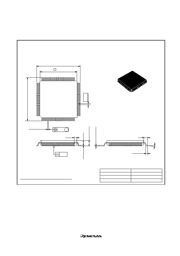
Rev. 2.0, 09/02, page 711 of 732
Appendix D Package Dimensions
0.10
23.2 ± 0.2
0.32 ± 0.08
0.65
1.6
0.8 ± 0.2
*
0.17 ± 0.05
3.05 Max
23.2 ± 0.2
84
57
56
29
112
1
28
20
85
2.70
0∞ ≠ 8∞
0.13 M
0.10
+0.15 ≠0.10
1.23
0.30 ± 0.06
0.15 ± 0.04
*
Hitachi Code
JEDEC
JEITA
Mass (reference value)
FP-112B
--
Conforms
2.4 g
*
Dimension including the plating thickness
Base material dimension
Unit: mm
Figure D.1 FP-112B
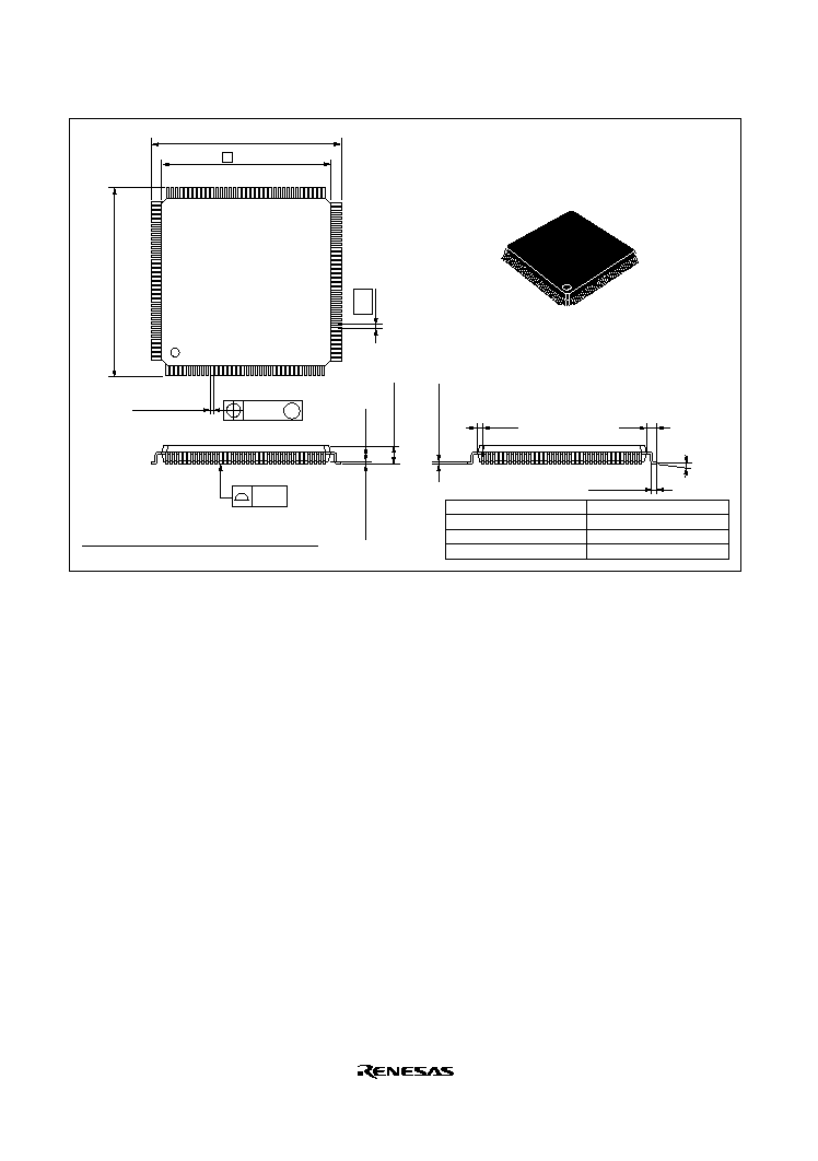
Rev. 2.0, 09/02, page 712 of 732
Hitachi Code
JEDEC
JEITA
Mass (reference value)
FP-144F
--
Conforms
1.4 g
*
Dimension including the plating thickness
Base material dimension
0.08
0.10
0.5
20
22.0 ± 0.2
108
73
109
72
37
144
1
36
22.0 ± 0.2
1.0
0.5 ± 0.1
1.70 Max
1.40
0.10 ± 0.10
0∞ ≠ 8∞
M
*
0.17 ± 0.05
*
0.22 ± 0.05
1.25
0.20 ± 0.04
0.15 ± 0.04
Unit: mm
Figure D.2 FP-144F
Rev. 2.0, 09/02, page 713 of 732
Main Revisions and Additions in this Edition
Item
Page
Revisions (See Manual for Details)
Features amended.
∑
On-chip
memory
ROM
Model
ROM
RAM
HD64F7144F50
256 kbytes
8 kbytes
Flash memory
Version
HD64F7145F50
256 kbytes
8 kbytes
HD647144F50
*
256 kbytes
8 kbytes
Mask ROM
Version
HD6437145F50
*
256 kbytes
8 kbytes
Note:
*
Under development
∑
I/O
ports
Model
No. of I/O Pins
No. of Input-only
Pins
HD64F7144F50/
HD6437144F50
*
74
8
HD64F7145F50/
HD6437145F50
*
98
8
Note:
*
Under development
∑
Compact
package
Model
Package
HD64F7144F50/HD64F7144F50
*
QFP-112
HD64F7145F50/HD6437145F50
*
LGFP-144
1.1 Features
2
Note:
*
Under development
Pin description added.
Type
Symbol
Name
Function
Clock
CK
System clock
output
Supplies the system clock to
external devices.
System
control
WDTOVF
Watchdog
timer
overflow
Output signal for the
watchdog timer overflow.
If this pin needs to be pulled-
down, the resistance value
must be 1 M
or higher.
1.4 Pin Functions
7, 8
Rev. 2.0, 09/02, page 714 of 732
Item
Page
Revisions (See Manual for Details)
Table 2.4 T Bit
20
Description amended.
ADD
#1, R0
ADD
#-1, R0
Execution states amended.
Instruction
Execution States
T Bit
BF/S label
2/1
*
2.5.1 Instruction Set by
Classification Branch
Instructions
38
Figure 2.4 Transitions
between Processing
States
41
Description amended.
Exception
processing state
When an internal power-on
reset by WDT or internal
manual reset by
WDT occurs
Exception
processing
Exception
processing
ends
NMI or IRQ interrupt
source occurs
= 1
= 1,
= 1
Bus request
cleared
Bus request
generated
3.1 Selection of
Operating Modes
43
Description added.
This LSI has four operating modes and four clock modes.
The operating mode is determined by the setting of MD3 to
MD0, and FWP pins. Do not change these pins during LSI
operation (while power is on). Do not set these pins in the
other way than the combination shown in table 3.1.
When power is applied to the system, be sure to conduct
power-on reset.
Table 3.2 Clock Mode
Setting
44
System clock output (CK) added.
4.3.1 Note on crystal
Resonator
50
Description amended.
A sufficient evaluation at the user's site is necessary to use
the LSI, by referring the resonator connection examples
shown in this section, because various characteristics related
to the crystal resonator are closely linked to the user's board
design. As the oscillator circuit's circuit constant external
circuit's component should be determined in consultation
with the resonator manufacturer. The design must ensure
that a voltage exceeding the maximum rating is not applied
to the oscillator pin.
Rev. 2.0, 09/02, page 715 of 732
Item
Page
Revisions (See Manual for Details)
4.3.2 Notes on Board
Design
51
Description added.
Measures against radiation noise are taken in this LSI. If
further reduction in radiation noise is needed, it is
recommended to use a multiple layer board and provide a
layer exclusive to the system ground.
When using a crystal oscillator, place the crystal oscillator
and its load capacitors
Separate the PLL power lines (PLLVcc, PLLVss) and the
system power lines (Vcc, Vss) at the board power supply
source, and be sure to insert bypass capacitors CB and CPB
close to the pins.
51, 52
Description added.
In principle, electromagnetic waves are emitted from an LSI
in operation. This LSI regards the lower of the system clock
(
) and the peripheral clock (P
) as fundamental (for
example, if
= 40 MHz and P
= 40 MHz, then 40 MHz), and
the peak of electromagnetic waves is in the high frequency
band. When this LSI is used adjacent to apparatuses
sensible to electromagnetic waves such as FM/VHF band
receivers, it is recommended to use a board with at least four
layers and provide a layer exclusive to the system ground.
Figure 8.1 Block
Diagram of DTC
104
Figure amended.
External
memory
External device
(memory-
mapped)
Interrupt request
Bus controller
External bus
Description amended.
Bit
Bit Name
Description
6
CHNE
DTC Chain Transfer Enable
When this bit is set to 1, a chain
transfer will be performed.
0: Chain transfer is canceled
1: Chain transfer is set
In data transfer with CHNE set to 1,
determination of the end of the
specified number of transfers, clearing
of the activation source flag, and
clearing of DTER is not performed.
8.2.1 DTC Mode
Register (DTMR)
107
Rev. 2.0, 09/02, page 716 of 732
Item
Page
Revisions (See Manual for Details)
Table 8.6 State Counts
Needed for Execution
State
122
Name amended.
Longword data read S
L
Longword data write S
L
8.4.3 DTC Use
Example
123
Description amended.
6. When DTCRA is 0 after the 128 data transfers have
ended, the RDRF flag is held at 1, the corresponding bit
in DTER is cleared to 0, and an RXI interrupt request is
sent to the CPU. The interrupt handling routine should
perform completion processing.
Figure 9.1 BSC Block
Diagram
126
Figure amended.
RAMER
On-chip memory
control unit
Table 9.2 Address Map
129
Address amended.
∑
On-chip ROM disabled mode
H'02000000 to H'FFFF7FFF
H'01000000 to H'FFFF7FFF
Figure 10.3 (1) Round
Robin Mode
166
Figure amended.
CH1
>
CH2
>
CH3
>
CH0
CH0
>
CH1
>
CH2
>
CH3
Transfer on channel 0
Initial priority setting
Priority after transfer
Channel 0 is given the lowest
priority.
11.1 Features
191
Features added.
∑
A total of six-phase waveform output, which includes
complementary PWM output, and positive and negative
phases of reset PWM output by interlocking operation of
channels 3 and 4, is possible.
∑
AC synchronous motor (brushless DC motor) drive mode
using complementary PWM output and reset PWM output
is settable by interlocking operation of channels 0, 3, and
4, and the selection of two types of waveform outputs
(chopping and level) is possible.
Rev. 2.0, 09/02, page 717 of 732
Item
Page
Revisions (See Manual for Details)
Descriptions added.
Item
Channel 0
Channel 1
Channel 2
Channel 3
Channel 4
PWM mode 2
--
--
Complementary
PWM mode
--
--
--
Reset PMW
mode
--
--
--
AC
synchronous
motor drive
mode
--
--
Phase counting
mode
--
--
--
Table 11.1 MTU
Functions
192
Table 11.10 TIORH_0
(channel 0) to Table
11.25 TIORL_4
(Channel 4)
205 to
220
Pin description amended.
Output prohibited
Output retained
Description added.
Legend:
X: Don't care
Note:
*
After power-on reset, 0 is output until TIOR is set.
Table 11.27 Output
Level Select Function
231
Bit No. amended.
Bit 1
Bit 0
Figure 11.30
Procedure for Selecting
the Reset-
Synchronized PWM
Mode
259
Figure amended.
Enable waveform output
Start count operation
Reset-synchronized PWM mode
[8]
[10]
Note: The output waveform starts to toggle operation at the point of
TCNT_3 = TGRA_3 = X by setting X = TGRA, i.e., cycle = duty.
[9]
PFC setting
[7] Set bits MD3-MD0 in TMDR_3 to B'1000 to select
the reset-synchronized PWM mode. Do not set to TMDR_4.
[8] Set the enabling/disabling of the PWM waveform output
pin in TOER.
[9] Set the port control register and the port I/O register.
[10] Set the CST3 bit in the TSTR to 1 to start the count
operation.
Figure 11.33 Example
of Complementary
PWM Mode Setting
Procedure
264
Figure amended.
Enable waveform output
Start count operation
<Complementary PWM mode>
[9] Select complementary PWM mode in timer mode register 3
(TMDR_3). Do not set in TMDR_4.
[10] Set enabling/disabling of PWM waveform output pin output in
the timer output master enable register (TOER).
[11] Set the port control register and the port I/O register.
[12] Set bits CST3 and CST4 in TSTR to 1 simultaneously to start
the count operation.
[10]
PFC setting
[11]
[12]

Rev. 2.0, 09/02, page 718 of 732
Item
Page
Revisions (See Manual for Details)
Figure 11.50 Example
of Output Phase
Switching by External
Input (1) to Figure 1.53
Example of Output
Phase Switching by
Means of UF, VF, WF
Bit Settings (2)
281,
282
Description amended.
When BCD = 1, N = 1, P = 1
When BDC = 1, N = 1, P = 1
Description added.
Channel
Name
Interrupt Source
4
TCIV_4
TCIV_4 overflow/underflow
Table 11.42 MTU
Interrupts
285
Figure 11.64 TGI
Interrupt Timing
(Compare Match)
291
Figure amended.
Compare
match signal
P
11.7.18 Cautions on
Transition from Normal
Operation or PWM
Mode 1 to Reset-
Synchronous PWM
Mode
305
Description amended.
When making a transition from normal operation to reset-
synchronous PWM mode, write H'11 to registers TIORH_3,
TIORL_3, TIORH_4, and TIORL_4 to initialize the output
pins to low level output, then set an initial register value of
H'00 before making the mode transition.
11.7.21 Simultaneous
Capture of TCNT_1
and TCNT_2 in
Cascade Connection
306
Description changed.
Figure 11.85 Error
Occurrence in Normal
Mode, Recovery in
Normal Mode to Figure
11.113 Error
Occurrence in Reset-
Synchronous PWM
Mode, Recovery in
Reset-Synchronous
PWM Mode
309 to
337
Description amended.
MTU output
MTU module output
Figure 11.115 Low-
Level Detection
Operation and Figure
11.116 Output-Level
Detection Operation
346
Symbol amended.
CK
P
Rev. 2.0, 09/02, page 719 of 732
Item
Page
Revisions (See Manual for Details)
11.9.5 Usage Note
347
Added.
Figure 12.1 Block
Diagram of WDT
350
Note added.
Overflow
Interrupt
control
ITI (interrupt
request signal)
Internal reset
signal
*
2
Reset
control
/2
/64
/128
/256
/512
/1024
/4096
/8192
Clock
Clock
select
Internal clock
sources
Notes: 1.
If this pin needs to be pulled-down,the resistance value must be 1M or higher.
2.
The internal reset signal can be generated by register setting.
Power-on reset or manual reset can be selected.
*
1
Table 13.3 BRR
Settings for Various Bit
Rates (Asynchronous
Mode) (4)
375
Note added.
Table 13.6 BRR
Settings for Various Bit
Rates (Clocked
Synchronous Mode) (1)
to (4)
378,
379
Setting values amended.
Table 13.7 Maximum
Bit Rate with External
Clock Input (Clocked
Synchronous Mode)
380
Note deleted.
Figure 13.7 Sample
Serial Transmission
Flowchart
387
Figure amended.
[1]
Initialization
Start transmission
[1] SCI initialization:
Set the TxD pin using the PFC.
After the TE bit is set to 1, a frame
period of 1s is output, and
transmission is enabled. This action
doesn't initiate immediate data
transmission.
Figure 13.8 Example of
SCI Operation in
Reception
388
Figure amended.
0
D0
D1
D7
0/1
1
0
D0
D1
D7
0/1
1
1
1
Data
Start
bit
Parity
bit
Stop
bit
Start
bit
Data
Parity
bit
Stop
bit
Idle state
(mark state)
RxD
Figure 13.11 Sample
Multiprocessor Serial
Transmission Flowchart
394
Figure amended.
[1]
Initialization
Start transmission
[1] SCI initialization:
Set the TxD pin using the PFC.
After the TE bit is set to 1, a
frame period of 1s is output, and
transmission is enabled. This
action doesn't initiate immediate
data transmission.
Rev. 2.0, 09/02, page 720 of 732
Item
Page
Revisions (See Manual for Details)
Figure 13.13 Sample
Multiprocessor Serial
Reception Flowchart (2)
397
Figure amended.
<End>
Clear ORER and
FER flags in SSR to 0
13.6.2 SCI initialization
(Clocked Synchronous
mode)
398
Title amended.
13.6.2 SCI initialization
13.6.2 SCI initialization (Clocked Synchronous mode)
14.5 Usage Notes
460
Usage notes added.
15.1 Features
463
Description added.
∑
Conversion time: 5.4 µs per channel (at P
= 25 MHz
operation), 6.7µs per channel (at P
= 20 MHz operation)
Figure 15.1 Block
Diagram of A/D
Converter (For One
Module)
464
Figure amended.
ADCR_0
ADCSR_0
ADDR0
ADDR1
ADDR2
ADDR3
: A/D0 control register
: A/D0 control/status register
: A/D0 data register 0
: A/D0 data register 1
: A/D0 data register 2
: A/D0 data register 3
: A/D1 control register
: A/D1 control/status register
: A/D1 data register 4
: A/D1 data register 5
: A/D1 data register 6
: A/D1 data register 7
ADCR_1
ADCSR_1
ADDR4
ADDR5
ADDR6
ADDR7
Legend:
Figure 15.2 A/D
Conversion Timing
473
Figure amended.
P
ADST write timing
Address
ADCSR
write
cycle
Internal write
signal
Table 15.3 A/D
Conversion Time
(Single Mode)
473
A/D conversion start delay time amended.
Rev. 2.0, 09/02, page 721 of 732
Item
Page
Revisions (See Manual for Details)
Figure 15.3 External
Trigger Input Timing
474
Figure amended.
CK
External trigger
signal
ADST
A/D conversion
Figure 15.6 Example of
Analog Input Circuit
477
Figure amended.
20 pF
10 k
C
in
=
20 pF
Sensor output
impedance of
up to 1 k
This LSI
Low-pass
filter
C = 0.1 F
Sensor input
A/D converter
equivalent circuit
Figure 16.8 CMCNT
Byte Write and
Increment Contention
488
Figure amended.
CMCNT
(Upper byte)
N
M
CMCNT
(Lower byte)
X
X
CMCNT write data
17.1.11 High-Current
Port Control Registers
(PPCR)
550
Description added.
The high-current port control register (PPCR) is an 8-bit
readable/writable register that is used to control six pins
(PE9/TIOC3B/SCK3/TRST
*
, PE11/TIOC3D/RXD3/TDO
*
,
PE12/TIOC4A/TXD3/TCK
*
, PE13/TIOC4B/MRES,
PE14/TIOC4C/DACK0, PE15/TIOC4D/DACK1/IRQOUT) of
the high-current ports.
This register is not supported in the emulator. Bits are always
read as undefined in the emulator.
17.2 Precautions for
Use
550
Usage note added.
Table 18.6 Port F Data
Register (PFDR)
Read/Write Operations
570
Bit No. amended.
Bits 15 to 0:
Bits 7 to 0:
19.6 On-Board
Programming Modes
581
Description amended.
When changing to boot mode, the boot program built into this
LSI is initiated. The boot program transfers the programming
control program from the externally-connected host to on-
chip RAM via SCI1. After erasing the entire flash memory,
the programming control program is executed.

Rev. 2.0, 09/02, page 722 of 732
Item
Page
Revisions (See Manual for Details)
Description amended.
Bit
Bit
Name
Description
0
SDTRF
Serial Data Transfer Control Flag
Indicates whether H-UDI registers can be
accessed by the CPU. The SDTRF bit is
initialized by the
TRST
signal, but is not
initialized in software standby mode.
0: Serial transfer to SDDR has ended,
and SDDR can be accessed
1: Serial transfer to SDDR is in progress
22.3.2 Status Register
(SDSR)
603
23.5.5 AUD Start-up
Sequence
620
Add.
24.3.1 Sleep Mode
Transition to Sleep
Mode
628
Description added.
Transition to Sleep Mode: If SLEEP instruction is executed
while the SSBY bit in SBYCR = 0, the CPU enters sleep
mode. In sleep mode, CPU operation stops, however the
contents of the CPU's internal registers are retained.
Peripheral functions except the CPU do not stop.
In sleep mode, data should not be accessed by the DMAC,
DTC, or AUD.
24.3.1 Sleep Mode
Clearing Sleep Mode
628
Description deleted.
∑
Clearing by an interrupt
∑
Clearing by DMAC/DTC address error
Description amended.
∑
Clearing by the power-on reset
When the
RES
pin is driven low, the CPU enters the
reset state. When the
RES
pin is driven high after the
elapse of the specified reset input period, the CPU starts
the reset exception handling.
When an internal Power-on reset by WDT occurs, sleep
mode is also cleared.
∑
Clearing by the manual reset
When the
MRES
pin is driven low while the
RES
pin is
high, the CPU shifts to the manual reset state and thus
sleep mode is cleared.
When an internal manual reset by WDT occurs, sleep
mode is also cleared.
Rev. 2.0, 09/02, page 723 of 732
Item
Page
Revisions (See Manual for Details)
24.3.2 Software
Standby Mode
630
Description amended.
∑
Clearing by the IRQ interrupt input
When the falling edge or rising edge of the
IRQ
pin
(selected by the IRQ7S to IRQ0S bits in ICR1 of the
interrupt controller (INTC) and the IRQ7ES[1:0] to
IRQ0ES[1:0] bits in ICR2) is detected, clock oscillation is
started
*
. This clock pulse is supplied only to the
watchdog timer (WDT). The IRQ interrupt priority level
should be higher than the interrupt mask level set in the
status register (SR) of the CPU before the transition to
software standby mode.
24.4.5 DMAC, DTC, or
AUD Operation in
Sleep Mode
632
Added.
Item, Min, Typ, and Max values, and Measurement
conditions amended.
Item
Symbol
Min
Typ
Max
Unit
Measurement
Conditions
RES
,
MRES
,
NMI, FWP, MD3
to MD0, DBGMD
V
IH
V
CC
-0.5
V
CC
+0.3
V
EXTAL
V
CC
-0.5
V
CC
+0.3
V
A/D port
2.2
AV
CC
+ 0.3
V
Input high-level
voltage (except
Schmitt trigger
input voltage)
Other input pins
2.2
V
CC
+0.3
V
V
T+
V
CC
-0.5
V
Schmitt trigger
input voltage
IRQ7
to
IRQ0
,
POE3
to
POE0
,
TCLKA to
V
T-
0.5
V
Output high-
level voltage
All output pins
V
OH
V
CC
-0.5
V
I
OH
= -200
µ
A
Output low-
level voltage
All output pins
V
OL
0.4
V
IOL = 1.6mA
RES
C
in
20
pF
Input
capacitance
NMI
20
pF
Vin = 0 V
f = 1 MHz
Ta = 25
∞
C
Clock
1:1
Icc
150
210
mA
f = 40 MHz
Current
consumption
*
2
Normal
operation
Clock
1:1/2
160
220
mA
f = 50 MHz
Clock
1:1
110
170
mA
f = 40 MHz
Sleep
Clock
1:1/2
120
180
mA
f = 50 MHz
Standby
3
50
µ
A
T
a
50
∞
C
500
µ
A
50
∞
C < T
a
Clock
1:1
150
210
mA
V
CC
= 3.3V
f = 40 MHz
Flash
program-
ming
Clock
1:1/2
160
220
mA
V
CC
= 3.3V
f = 50MHz
Table 26.2 DC
Characteristics
666,
667
Rev. 2.0, 09/02, page 724 of 732
Item
Page
Revisions (See Manual for Details)
Item, Min, Typ, and Max values, and Measurement conditions
amended.
Item
Symbol
Min
Typ
Max
Unit
Measurement
Conditions
During A/D
conversion
AI
CC
2
5
mA
Waiting for A/D
conversion
2
mA
Analog Power
supply current
Standby
5
µ
A
During A/D
conversion
AI
ref
2
mA
Waiting for A/D
conversion
2
mA
Reference
power supply
current
Standby
5
µ
A
Table 26.2 DC
Characteristics
667
Min and Max values amended.
Item
Symbol
Min
Max
Clock low-level pulse width
t
CL
1/2 t
cyc
-
5
Clock high-level pulse width
t
CH
1/2 t
cyc
-
5
Clock rise time
t
CR
5
Clock fall time
t
CF
5
Table 26.4 Clock
Timing
670
Item, and Min and Max values amended.
Item
Symbol
Min
Max
RES
pulse width
t
RESW
25
MRES
pulse width
t
MRESW
20
MRES
setup time
t
MRESS
35
MD3 to MD0 setup time
t
MDS
20
IRQ7
to
IRQ0
setup time
*
(edge detection)
t
IRQES
19
IRQ7
to
IRQ0
setup time
*
(level detection)
t
IRQLS
19
IRQ7
to
IRQ0
hold time
t
IRQEH
19
IRQOUT
output delay time
t
IRQOD
100
Bus request setup time
t
BRQS
19
Table 26.5 Control
Signal Timing
672

Rev. 2.0, 09/02, page 725 of 732
Item
Page
Revisions (See Manual for Details)
Min and Max values amended.
Item
Symbol
Min
Max
Write data delay time
t
WDD
30
WAIT
setup time
t
WTS
12
WAIT
hold time
t
WTH
3
Read data access
time
t
ACC
t
cyc
◊
(n+2)
-
35
Access time from
read strobe
t
OE
t
cyc
◊
(n+1.5)
-
33
Table 26.6 Bus Timing
675
Item and Min values amended.
Item
Symbol
Min
Max
DREQ0
,
DREQ1
setup
time
t
DRQS
10
DREQ0
,
DREQ1
hold time
t
DRQH
1.5 t
cyc
-
10
Table 26.7 Direct
Memory Access
Controller Timing
679
Min values amended.
Item
Symbol
Min
Max
Input capture input setup time
t
TICS
19
Timer input setup time
t
TCKS
19
Table 26.8 Multi-
Function Timer Pulse
Unit Timing
681
Min values description of operating precautions amended.
Item
Symbol
Min
Port output data delay time
t
PWD
Port input hold time
t
PRH
19
Port input setup time
t
PRS
19
Table 26.9 I/O Port
Timing
682
[Operating precautions]
The port input signals are asynchronous. They are, however,
considered to have been changed at CK clock fall with two-
state intervals shown in figure 26.17. If the setup times
shown here are not observed, recognition may be delayed
until the clock fall two states after that timing.
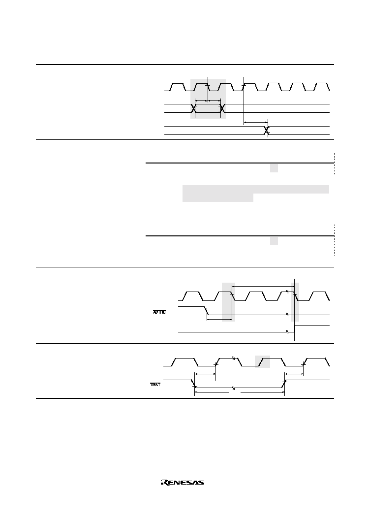
Rev. 2.0, 09/02, page 726 of 732
Item
Page
Revisions (See Manual for Details)
Figure 26.17 I/O Port
Input/Output timing
682
Figure amended.
t
PRS
t
PRH
t
PWD
CK
Port
(read)
Port
(write)
Min values and description of notes amended.
Item
Symbol
Min
Typ
Max
Data input setup time
t
SDAS
35
Table 26.12 I
2
C Bus
Interface Timing
686
Notes: 1.
t
pcyc
(ns) = 1/(P
supplied to I
2
C module (MHz) )
2. Can be set to 17.5 t
pcyc
by selecting the clock to be
used for the I
2
C module. For details, refer to
section 14.5, Usage Notes.
Min values amended.
Item
Symbol
Min
Typ
Max
External trigger input start
delay time
t
TRGS
50
--
--
Table 26.14 A/D
Converter Timing
688
Figure 26.23 External
Trigger Input Timing
688
Figure amended.
CK
input
ADCRn Register
(ADST = 1 set)
3≠5 states
t
TRGS
V
OH
Figure 26.25 H-UDI
TRST
Timing
689
Figure amended.
t
TRSS
t
TRSS
V
IL
V
IL
V
IH
V
IL
TCK
t
TRSW

Rev. 2.0, 09/02, page 727 of 732
Item
Page
Revisions (See Manual for Details)
Min and Max values amended.
Item
Symbol
Min
Max
Branch trace data delay time
t
BTDD
11
Branch trace data hold time
t
BTDH
-
10
Branch trace SYNC delay time
t
BTSD
10
Branch trace SYNC hold time
t
BTSH
-
10
RAM monitor input data setup
time
t
RMDS
10
RAM monitor input data hold time
t
RMDH
15
RAM monitor SYNC setup time
t
RMSS
10
RAM monitor SYNC hold time
t
RMSH
13
Table 26.16 AUD
Timing
691
Max values amended and description of notes added.
Item
Min
Max
Non-linear error
--
±
3.0
*
3
*
4
*
5
/
±
5.0
*
6
Offset error
--
±
3.0
*
3
*
4
*
5
/
±
5.0
*
6
Full-scale error
--
±
3.0
*
3
*
4
*
5
/
±
5.0
*
6
Absolute error
--
±
4.0
*
3
*
4
*
5
/
±
6.0
*
6
Table 26.17 A/D
Converter
Characteristics
693
Notes: 1.
This is a value when (CKS1, 0) = (1,1) and t
pcyc
= 50 ns.
2.
This is a value when (CKS1, 0) = (1,1) and t
pcyc
= 40 ns.
3.
This is a value when (CKS1, 0) = (1,1), t
cyc
= 50 ns, and
T
a
=
-
20 to
+
75
∞
C (regular specifications).
4.
This is a value when (CKS1, 0) = (1,1), t
pcyc
= 40 ns, and
T
a
=
-
20 to
+
75
∞
C (regular specifications).
5.
This is a value when (CKS1, 0) = (1,1), t
pcyc
= 50 ns, and
T
a
=
-
40 to
+
85
∞
C (wide-range specifications).
6.
This is a value when (CKS1, 0) = (1,1), t
pcyc
= 40 ns, and
T
a
=
-
40 to
+
85
∞
C (wide-range specifications).
Min, Typ, and Max values amended and description of notes
added.
Item
Symbol
Min
Typ
Max
Reprogramming
count
N
WEC
100
6
10000
7
--
Table 26.18 Flash
Memory Characteristics
694,
695
Notes: 6.
The minimum times that all characteristics after rewriting
are guaranteed. (A range between 1 and minimum value
is guaranteed.)
7.
The reference value at 25∞C. (Normally, it is a reference
that rewriting is enabled up to this value.)

Rev. 2.0, 09/02, page 728 of 732
Item
Page
Revisions (See Manual for Details)
Description amended.
Product Type
Product Code
Package
(Hitachi Package Code)
SH7144
Flash memory version
Standard product
HD64F7144F50
QFP-112 (FP-112B)
Mask ROM version
Standard product
HD6437144F50
*
QFP-112 (FP-112B)
SH7145
Flash memory version
Standard product
HD64F7144F50
LQFP-144 (FP-144F)
Mask ROM version
Standard product
HD6437144F50
*
LQFP-144 (FP-144F)
Appendix C Product
Code Lineup
710
Note:
*
Under development

Rev. 2.0, 09/02, page 729 of 732
Index
A/D conversion time ............................... 472
A/D converter ......................................... 463
Activation by interrupt............................ 122
Activation by software............................ 123
Address error exception processing .......... 60
Address map ..................................... 46, 128
Addressing modes..................................... 22
Advanced user debugger (AUD)............. 611
Asynchronous serial communication ...... 381
Auto-request mode.................................. 163
Block configuration ................................ 576
Block transfer mode................................ 118
Boot mode............................................... 582
Branch trace mode .................................. 614
Buffer operation...................................... 242
Burst mode.............................................. 175
Bus arbitration ........................................ 144
Bus masters ............................................. 144
Bus release state........................................ 42
Bus state controller (BSC) ...................... 125
Byte data ................................................... 17
Cascaded operation ................................. 245
Chain transfer.......................................... 119
Clock mode ............................................... 44
Clock pulse generator ............................... 47
Clocked synchronous communication .... 398
Compare match ....................................... 237
Compare match timer (CMT) ................. 481
Complementary PWM mode .................. 261
Continuous scan mode ............................ 471
Control registers........................................ 15
CPU .......................................................... 13
Crystal oscillator ....................................... 48
Cycle-steal mode..................................... 175
Data format in registers............................. 17
Data formats.............................................. 17
Data formats in memory ........................... 17
Data transfer controller (DTC)................103
Delayed branch instructions ......................19
Direct memory access controller (DMAC)
................................................................149
DTC vector addresses .............................113
Dual address mode ..................................170
Effective address .......................................22
Electrical characteristics..........................665
Error Protection.......................................592
Exception processing ................................53
Exception processing state ........................42
Exception processing vector table.............55
External clock input ..................................49
External request mode.............................163
Fixed mode..............................................165
Flash memory..........................................571
Flash memory emulation in RAM...........585
Free-running counters .............................236
Function for detecting the oscillator halt...50
Functions of multiplexed pins .................489
General illegal instructions .......................63
General registers (Rn) ...............................13
Global base register (GBR) .......................16
Hardware protection................................591
Hitachi user debug interface (H-UDI).....599
Hitachi user debug interface (H-UDI)
interrupt.....................................................78
I/O ports ..................................................553
I
2
C bus format .........................................435
I
2
C bus interface......................................411
Illegal slot instructions ..............................63
Immediate data format ..............................18
Input capture function .............................239
Internal clock.............................................47
Interrupt controller (INTC) .......................67

Rev. 2.0, 09/02, page 730 of 732
Interrupt exception processing.................. 61
Interrupt response time ............................. 85
Interval timer mode................................. 355
IRQ interrupts ..................................... 74, 77
Longword data .......................................... 17
Manual reset ............................................. 58
Mask ROM ............................................. 595
Master device.......................................... 437
MCU operating modes.............................. 43
Module standby mode............................. 631
Multi-function timer pulse unit (MTU) .. 191
Multiply-and-accumulate registers
(MAC) ...................................................... 16
Multiprocessor communication
function................................................... 392
NMI interrupts .......................................... 77
Normal mode .......................................... 117
On-board programming modes ............... 581
On-chip peripheral module interrupts ....... 78
On-chip peripheral module request mode163
Permissible signal source impedance...... 479
Phase counting mode .............................. 252
Pin function controller (PFC) ................. 489
Port output enable (POE)........................ 338
Power-down modes ................................ 621
Power-down state...................................... 42
Power-on reset .......................................... 57
Procedure register (PR)............................. 16
Processing states ....................................... 41
Program counter (PC) ............................... 16
Program execution state............................ 42
PWM mode............................................. 247
RAM ....................................................... 597
RAM emulation ...................................... 585
RAM monitor mode................................ 615
Reading from TCNT, TCSR,
and RSTCSR........................................... 358
Register
ADCR ......................... 468, 640, 653, 663
ADCSR ....................... 467, 640, 653, 662
ADDR ......................... 466, 640, 652, 662
ADTSR ....................... 470, 643, 657, 664
BCR1 .......................... 130, 642, 654, 663
BCR2 .......................... 132, 642, 654, 663
BRR ............................ 373, 634, 645, 658
CHCR.......................... 153, 642, 655, 663
CMCNT ...................... 484, 640, 652, 662
CMCOR ...................... 484, 640, 652, 662
CMCSR....................... 483, 640, 652, 662
CMSTR ....................... 482, 640, 652, 662
DAR ............................ 152, 642, 655, 663
DMAOR...................... 159, 642, 654, 663
DMATCR ................... 153, 642, 655, 663
DTBR.......................... 111, 643, 657, 664
DTCRA ............................................... 108
DTCRB ............................................... 109
DTCSR........................ 110, 643, 657, 664
DTDAR............................................... 108
DTER .......................... 109, 643, 657, 664
DTIAR ................................................ 108
DTMR ................................................. 106
DTSAR ............................................... 108
EBR1........................... 579, 641, 653, 663
EBR2........................... 580, 641, 653, 663
FLMCR1 ..................... 577, 641, 653, 663
FLMCR2 ..................... 579, 641, 653, 663
ICCR ........................... 421, 644, 657, 664
ICDR ........................... 414, 644, 657, 664
ICMR .......................... 418, 644, 657, 664
ICR1.............................. 70, 638, 649, 661
ICR2.............................. 72, 638, 650, 661
ICSR.................................... 429, 644, 657
ICSR1.......................... 340, 639, 651, 662
IPR ................................ 75, 638, 649, 661
ISR ................................ 74, 638, 649, 661
MSTCR ....................... 626, 641, 654, 663
OCSR .......................... 344, 639, 651, 662
PACR .......................... 517, 638, 650, 661
PADR.......................... 555, 638, 650, 661
PAIOR......................... 516, 638, 650, 661

Rev. 2.0, 09/02, page 731 of 732
PBCR .......................... 526, 639, 650, 661
PBDR.......................... 557, 638, 650, 661
PBIOR ........................ 525, 638, 650, 661
PCCR .......................... 529, 639, 651, 661
PCDR.......................... 559, 638, 650, 661
PCIOR......................... 529, 638, 650, 661
PDCR.......................... 532, 639, 651, 662
PDDR.......................... 563, 639, 651, 662
PDIOR ........................ 531, 639, 651, 662
PECR .......................... 543, 639, 651, 662
PEDRL........................ 567, 639, 651, 662
PEIORL ...................... 542, 639, 651, 662
PFDR .......................... 569, 639, 651, 662
PPCR .......................... 550, 643, 657, 664
RAMER .............. 137, 580, 642, 654, 663
RDR ............................ 365, 634, 645, 658
RSR..................................................... 365
RSTCSR ..................... 353, 641, 654, 663
SAR (DMAC) ............. 152, 642, 655, 663
SAR (IIC).................... 416, 644, 657, 664
SARX.......................... 417, 644, 657, 664
SBYCR ....................... 623, 641, 654, 663
SCR............................. 367, 634, 645, 658
SCRX.......................... 434, 643, 657, 664
SDBPR................................................ 604
SDCR.......................... 372, 634, 645, 658
SDDR.......................... 604, 644, 657, 664
SDIR ........................... 602, 644, 657, 664
SDSR .......................... 603, 644, 657, 664
SMR............................ 366, 634, 645, 658
SSR ............................. 369, 634, 645, 658
SYSCR........................ 625, 641, 654, 663
TCBR.......................... 234, 635, 647, 659
TCDR.......................... 234, 635, 646, 659
TCNT (MTU) ............. 226, 635, 646, 660
TCNT (WDT) ............. 351, 641, 654, 663
TCNTS........................ 233, 635, 647, 659
TCR ............................ 198, 635, 646, 659
TCSR .......................... 351, 641, 654, 663
TDDR ......................... 233, 635, 646, 659
TDR ............................ 365, 634, 645, 658
TGCR.......................... 231, 635, 646, 659
TGR ............................ 226, 635, 647, 659
TIER............................ 221, 635, 646, 659
TIOR ........................... 203, 635, 646, 659
TMDR ......................... 202, 635, 646, 659
TOCR .......................... 230, 635, 646, 659
TOER .......................... 229, 635, 646, 659
TSR (MTU)................. 223, 636, 647, 659
TSR (SCI) ...........................................365
TSTR........................... 227, 636, 647, 659
TSYR .......................... 227, 636, 647, 659
UBAMR ........................ 93, 641, 653, 663
UBAR ........................... 93, 641, 653, 663
UBBR............................ 94, 641, 653, 663
UBCR............................ 95, 641, 653, 663
WCR1 ......................... 136, 642, 654, 663
WCR2 ......................... 137, 642, 654, 663
Register address table..............................633
Register bit list ........................................645
Register states in each operating mode ...658
Repeat mode............................................117
Reset state .................................................42
Reset-synchronized PWM mode.............258
RISC-type .................................................18
Round robin mode...................................165
Serial communication interface (SCI).....361
Serial format............................................435
Single address mode................................168
Single mode.............................................471
Single-cycle scan mode...........................472
Slave device ............................................442
Sleep mode..............................................628
Software protection .................................592
Software standby mode ...........................629
Status register (SR) ...................................15
Synchronous operation............................240
System clock (
) .......................................47
System registers ........................................16
Trap instructions .......................................62
User break controller (UBC) .....................91
User break interrupt...................................78
User program mode.................................584

Rev. 2.0, 09/02, page 732 of 732
Vector base register (VBR)....................... 16
Vector No. .................................... 79, 80, 81
Vectors table ............................................. 79
Watchdog timer ...................................... 349
Watchdog timer mode............................. 354
Word data.................................................. 17
Writing to RSTCSR ................................ 358
Writing to TCNT and TCSR ................... 357

SH7144 Series Hardware Manual
Publication Date: 1st Edition, September 2001
2nd Edition, September 2002
Published by:
Business Operation Division
Semiconductor & Integrated Circuits
Hitachi, Ltd.
Edited by:
Technical Documentation Group
Hitachi Kodaira Semiconductor Co., Ltd.
Copyright © Hitachi, Ltd., 2001. All rights reserved. Printed in Japan.