Philips Semiconductors
Product specification
74F821/822/823/824/825/826
Bus interface registers
2
1996 Jan 05
853-1304 16195
74F821
10-bit bus interface register, non-inverting (3-State)
74F822
10-bit bus interface register, inverting (3-State)
74F823
9-bit bus interface register, non-inverting (3-State)
74F824
9-bit bus interface register, inverting (3-State)
74F825
8-bit bus interface register, non-inverting (3-State)
74F826
8-bit bus interface register, inverting (3-State)
FEATURES
∑
High speed parallel registers with positive edge-triggered D-type
flip-flops
∑
High performance bus interface buffering for wide data/address
paths or busses carrying parity
∑
High impedance PNP base inputs for reduced loading (20
µ
A in
high and low states)
∑
I
IL
is 20
µ
A vs 1000
µ
A for AM29821 series
∑
Buffered control inputs to reduce AC effects
∑
Ideal where high speed, light loading, or increased fan-in as
required with MOS microprocessor
∑
Positive and negative over-shoots are clamped to ground
∑
3-State outputs glitch free during power-up and power-down
∑
Slim Dip 300 mil package
∑
Broadside pinout compatible with AMD AM 29821-29826 series
∑
Outputs sink 64mA and source 24mA
∑
Industrial temperature range available (≠40
∞
C to +85
∞
C) for
74F823
DESCRIPTION
The 74F821 series bus interface registers are designed to
eliminate the extra packages required to buffer existing registers and
provide extra data width for wider data/address paths of busses
carrying parity.
The 74F821/74F822 are buffered 10-bit wide versions of the popular
74F374/74F534 functions.
The 74F822 is the inverted output version of 74F821.
The 74F823 and 74F824 are 9-bit wide buffered registers with clock
enable (CE) and master reset (MR) which are ideal for parity bus
interfacing in high microprogrammed systems.
The 74F824 is the inverted version of 74F823.
The 74F825 and 74F826 are 8-bit buffered registers with all the
74F823/74F824 controls plus output enable (OE0, OE1, OE2) to
allow multiuser control of the interface, e.g., CS, DMA, and RD/WR.
They are ideal for uses as an output port requiring high I
OL
/I
OH
.
The 74F826 is the inverted version of 74F825.
TYPE
TYPICAL
f
max
TYPICAL
SUPPLY CURRENT
(TOTAL)
74F821, 74F822
180MHz
75mA
74F823, 74F824
180MHz
70mA
74F825, 74F826
180MHz
65mA
ORDERING INFORMATION
ORDER CODE
DESCRIPTION
COMMERCIAL RANGE
V
CC
= 5V
±
10%,
T
amb
= 0
∞
C to +70
∞
C
INDUSTRIAL RANGE
V
CC
= 5V
±
10%,
T
amb
= ≠40
∞
C to +85
∞
C
PKG. DWG. #
24-pin plastic slim DIP (300mil)
N74F821N, N74F822N, N74F823N,
N74F824N, N74F825N, N74F826N
I74F823N
SOT222-1
24-pin plastic SOL
N74F821D, N74F822D, N74F823D,
N74F824D, N74F825D, N74F826D
I74F823D
SOT137-1

Philips Semiconductors
Product specification
74F821/822/823/824/825/826
Bus interface registers
1996 Jan 05
3
INPUT AND OUTPUT LOADING AND FAN OUT TABLE
PINS
DESCRIPTION
74F (U.L.)
HIGH/LOW
LOAD VALUE
HIGH/LOW
Dn
Data inputs
1.0/1.0
20
µ
A/0.6mA
74F821
CP
Clock input
1.0/1.0
20
µ
A/0.6mA
74F822
OE
Output enable input (active low)
1.0/3.0
20
µ
A/1.8mA
Qn, Qn
Data outputs
1200/106.7
24mA/64mA
Dn
Data inputs
1.0/1.0
20
µ
A/0.6mA
CP
Clock input
1.0/1.0
20
µ
A/0.6mA
74F823
CE
Clock enable input (active low)
1.0/3.0
20
µ
A/1.8mA
74F824
MR
Master reset input (active low)
1.0/3.0
20
µ
A/1.8mA
OE
Output enable input (active low)
1.0/3.0
20
µ
A/1.8mA
Qn, Qn
Data outputs
1200/106.7
24mA/64mA
Dn
Data inputs
1.0/1.0
20
µ
A/0.6mA
CP
Clock input
1.0/1.0
20
µ
A/0.6mA
74F825
CE
Clock enable input (active low)
1.0/3.0
20
µ
A/1.8mA
74F826
MR
Master reset input (active low)
1.0/3.0
20
µ
A/1.8mA
OE
Output enable input (active low)
1.0/3.0
20
µ
A/1.8mA
Qn, Qn
Data outputs
1200/106.7
24mA/64mA
NOTE: One (1.0) FAST unit load is defined as: 20
µ
A in the high state and 0.6mA in the low state.
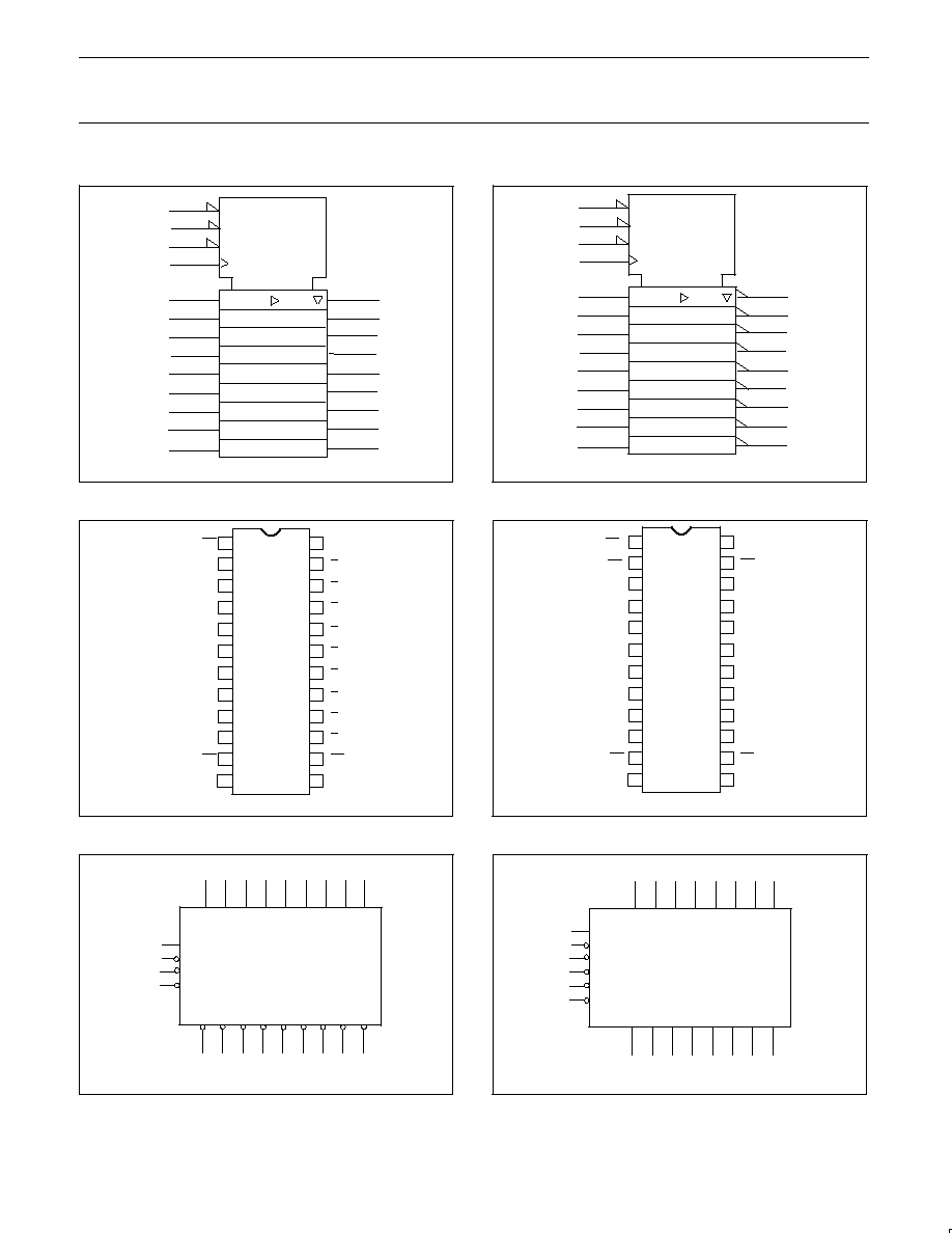
PIN CONFIGURATION ≠ 74F821
24
23
22
21
20
19
18
17
16
15
14
13
12
10
11
9
8
7
6
5
4
3
2
1
GND
OE
CP
Q0
Q3
Q4
Q5
Q6
V
CC
Q7
Q1
Q2
Q8
Q9
D0
D3
D4
D5
D6
D7
D1
D2
D8
D9
SF00482
LOGIC SYMBOL ≠ 74F821
CP
OE
Q0 Q1 Q2 Q3 Q4 Q5 Q6 Q7
13
1
D0 D1 D2 D3 D4 D5 D6 D7
2
3
4
5
6
7
8
9
23
22
21
20
19
18
17
16
V
CC
= Pin 24
GND = Pin 12
D8 D9
10
11
Q8 Q9
15
14
SF00483