1999 Dec 10
2
Philips Semiconductors
Product specification
Schottky barrier diode
1PS74SB43
FEATURES
∑
Ultra fast switching speed
∑
Low forward voltage
∑
Fast recovery time
∑
Guard ring protected
∑
Small plastic SMD package
∑
Capability of absorbing very high
surge current.
APPLICATIONS
∑
Rectification
∑
Circuit protection
∑
Polarity protection
∑
Switched-mode power supplies.
DESCRIPTION
Planar Schottky barrier diode
encapsulated in an SC-74 (SOT457)
small plastic SMD package.
PINNING
PIN
DESCRIPTION
1
anode
2
cathode
3
anode
4
anode
5
cathode
6
anode
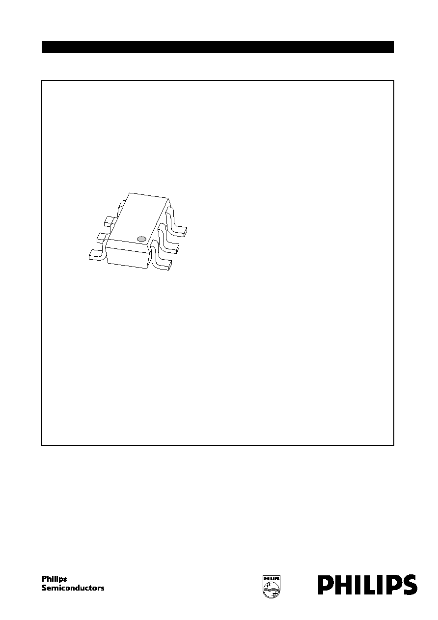
Fig.1 Simplified outline SC-74 (SOT457) and symbol.
Marking code: P2.
handbook, halfpage
MAM421
Top view
1, 3,
4, 6
2, 5
1
3
2
4
5
6
LIMITING VALUES
In accordance with the Absolute Maximum Rating System (IEC 134).
Note
1. Pins 1, 3, 4 and 6 are connected in parallel; pins 2 and 5 are connected in parallel.
SYMBOL
PARAMETER
CONDITIONS
MIN.
MAX.
UNIT
V
R
continuous reverse voltage
-
40
V
I
F
continuous forward current
-
1
A
I
FSM
non-repetitive peak forward current
tp
=
8.3 ms; half sinewave;
JEDEC method; note 1
-
27
A
I
RSM
non-repetitive peak reverse current
tp = 100
µ
s
-
0.5
A
T
stg
storage temperature
-
65
+150
∞
C
T
j
junction temperature
-
125
∞
C

1999 Dec 10
3
Philips Semiconductors
Product specification
Schottky barrier diode
1PS74SB43
ELECTRICAL CHARACTERISTICS
T
amb
= 25
∞
C unless otherwise specified.
Note
1. Pulsed test: t
p
= 300
µ
s;
= 0.02.
THERMAL CHARACTERISTICS
Note
1. Refer to SC-74 (SOT457) standard mounting conditions.
SYMBOL
PARAMETER
CONDITIONS
TYP.
MAX.
UNIT
V
F
continuous forward voltage
see Fig.2; note 1
I
F
= 0.1 A
280
330
mV
I
F
= 1 A
460
500
mV
I
R
continuous reverse current
V
R
= 10 V; note 1; see Fig.3
15
40
µ
A
V
R
= 40 V; note 1; see Fig.3
60
300
µ
A
C
d
diode capacitance
V
R
= 4 V; f = 1 MHz; see Fig.4
65
80
pF
SYMBOL
PARAMETER
CONDITIONS
VALUE
UNIT
R
th j-a
thermal resistance from junction to ambient
note 1
200
K/W

1999 Dec 10
4
Philips Semiconductors
Product specification
Schottky barrier diode
1PS74SB43
GRAPHICAL DATA
handbook, halfpage
0.6
VF (V)
IF
(mA)
0
0.2
(2) (3)
(4)
(1)
0.4
10
3
10
2
10
1
MGL923
Fig.2
Forward current as a function of forward
voltage; typical values.
(1) T
amb
= 125
∞
C.
(2) T
amb
= 100
∞
C.
(3) T
amb
= 75
∞
C.
(4) T
amb
= 25
∞
C.
handbook, halfpage
10
4
10
2
10
3
10
1
0
MLC389
30
20
10
40
(4)
(1)
(2)
(3)
V (V)
I R
(
µ
A)
R
Fig.3
Reverse current as a function of reverse
voltage; typical values.
(1) T
amb
= 125
∞
C.
(2) T
amb
= 100
∞
C.
(3) T
amb
= 75
∞
C.
(4) T
amb
= 25
∞
C.
handbook, halfpage
10
3
10
2
10
0
MLC390
16
24
32
8
40
V (V)
R
C d
(pF)
Fig.4
Diode capacitance as a function of reverse
voltage; typical values.
f = 1 MHz; T
amb
= 25
∞
C.