 | ÐлекÑÑоннÑй компоненÑ: DN8798MS | СкаÑаÑÑ:  PDF PDF  ZIP ZIP |
DN8798MS
Hall ICs
1
Publication date: November 2002
SPC00008CJB
DN8798MS
3 V operation Hall IC
Alternating magnetic field operation
Overview
The DN8798MS is a 3 V operation Hall IC which
includes a Hall element, amplifier circuit, Schmidt circuit,
stabilized power supply and temperature compensation cir-
cuit which are integrated on a single chip with a fine pat-
terning technology. The magnetic input signal is output-
ted by being converted to high or low. We have improved
the conventional circuit to realize a stable operation cov-
ering from low to high supply voltage and from low to
high temperature.
Features
· Wide operating supply voltage range
(V
CC
= 2.7 V to 14.4 V)
· Wide operating ambient temperature (-40°C to +85°C)
· Package: Mini type (3-pin type)
(1.1 mm thick: Same as a standard transistor)
· Open collector output
Applications
· DC brushless motor, fan motor, rotation sensor, detec-
tion of cover open/close (example for a cellular phone),
position sensor
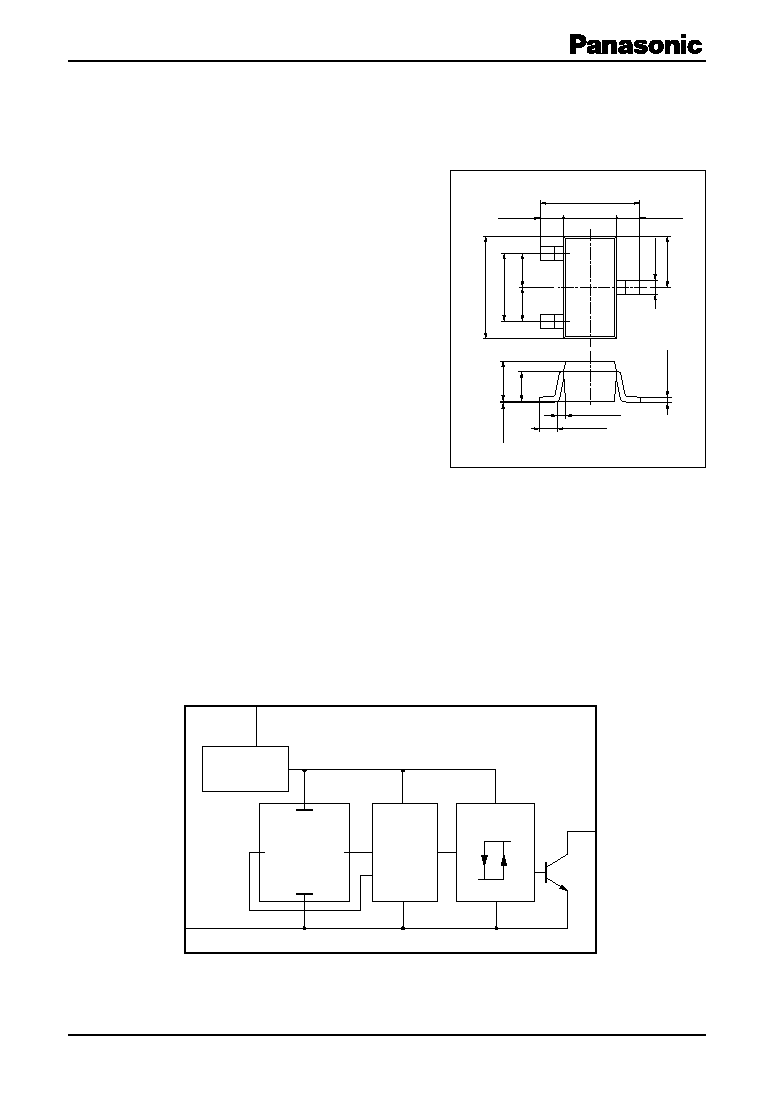
Block Diagram
Unit: mm
MINI-3D
2
V
CC
1
Out
3
GND
Constant
voltage source
Hall element
Amplifier
Comparator
2.80
+0.20
0.30
1.50
+0.25
0.05
0.65±0.15
0.65±0.15
3
1
2
0.95
0.95
1.90±0.20
0.40
+0.10 0.05
1.10
+0.20 0.10
0.80
0.40±0.20
0.16
+0.10 0.06
1.45
0.10 to 0.30
2.90
+0.20 0.05
0 to 0.10
Note) The package of this product will be changed
to lead-free type (MINI-3DA). See the new
package dimensions section later of this
datasheet.
2
DN8798MS
SPC00008CJB
Note) 1. Symbol B
H-L
stands for the operating magnetic flux density where its output level varies from high to low.
2. Symbol B
L-H
stands for the operating magnetic flux density where its output level varies from low to high.
3. The variation of operating magnetic flux density does not depend on supply voltage due to its built-in stabilized power
source. (V
CC
should be confined to the range of 2.7 V to 14.4 V.)
4. A supply current changes by maximum 1 mA when its output level varies from high to low.
Pin Descriptions
Pin No.
Symbol
Description
1
Out
Output pin
2
V
CC
Supply voltage pin
3
GND
Ground pin
Recommended Operating Range
Parameter
Symbol
Range
Unit
Supply voltage
V
CC
2.7 to 14.4
V
Absolute Maximum Ratings
Parameter
Symbol
Rating
Unit
Supply voltage
V
CC
18
V
V
OUT
18
Supply current
I
CC
mA
Power dissipation
P
D
120
mW
Operating ambient temperature
T
opr
-40 to +85
°C
Storage temperature
T
stg
-55 to +125
°C
Note) 1. Except for the operating ambient temperature and storage temperature, all ratings are for T
a
= 25°C.
2. The reverse insertion of this IC will cause its breakdown.
3. It will operate normally in several tens of ms after power on.
4. This IC is not suitable for car electrical equipment.
Electrical Characteristics at T
a
= 25°C
Parameter
Symbol
Conditions
Min
Typ
Max
Unit
Operating magnetic flux density 1
B
H-L
V
CC
= 3 V
-15
mT
Operating magnetic flux density 2
B
L-H
V
CC
= 3 V
15
mT
Hysteresis width
BW
V
CC
= 3 V
4
8
12
mT
Output voltage 1
V
OL1
V
CC
= 14.4 V, I
O
= 5 mA, B = -15 mT
0.07
0.30
V
Output voltage 2
V
OL2
V
CC
= 2.7 V, I
O
= 5 mA, B = -15 mT
0.07
0.30
V
Output current
I
OH
V
CC
= 2.7 V to 14.4 V
10
µA
V
O
= 14.4 V, B = 15 mT
Supply current 1
I
CC1
V
CC
= 14.4 V, B = 15 mT
1.0
3.4
6.0
mA
Supply current 2
I
CC2
V
CC
= 2.7 V, B = 15 mT
1.0
2.5
6.0
mA
3
DN8798MS
SPC00008CJB
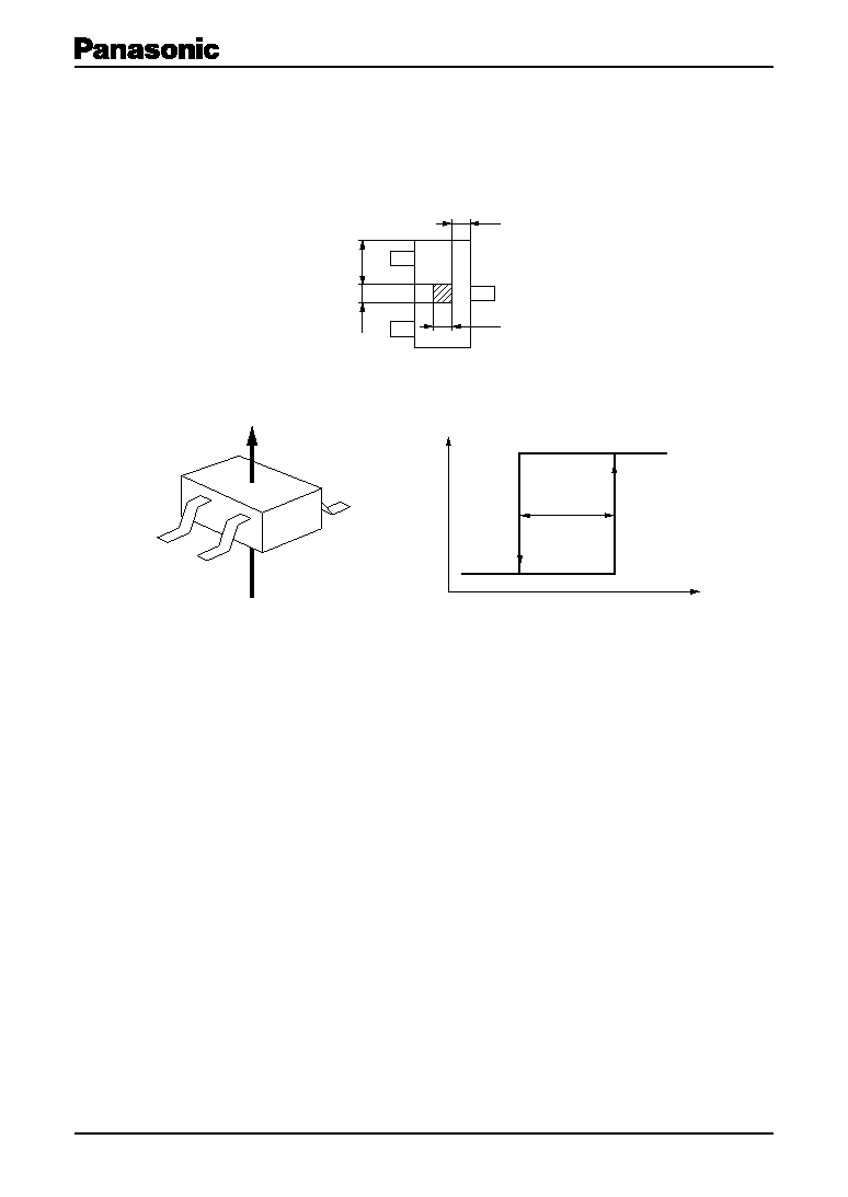
Technical Data
· Position of a Hall element (unit in mm)
Distance from a package surface to sensor part: 0.71 mm
A Hall element is placed on the shaded part in the figure.
0.5
0.5
1.2
0.5
· Magneto-electro conversion characteristics
Direction of applied magnetic field
Applied magnetic flux density B
Output v
oltage
S
N
BW
B
H-L
B
L-H
4
DN8798MS
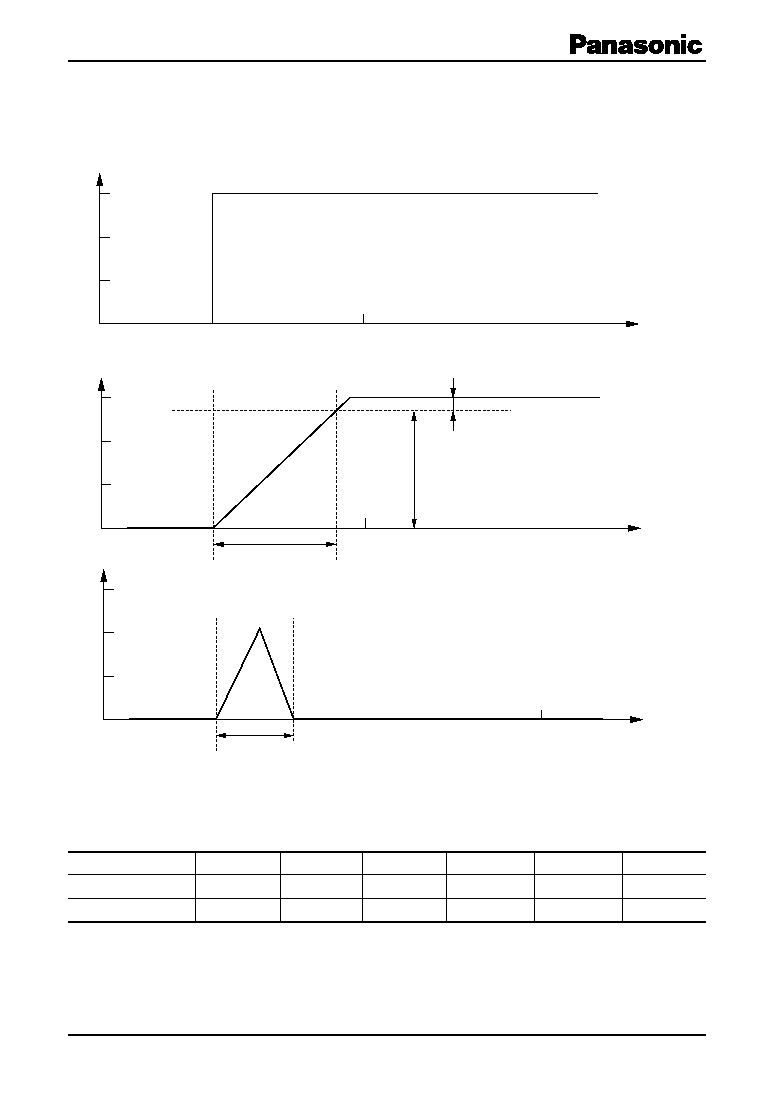
SPC00008CJB
V
CC
=
3.0 V, Pull-Up-R.
= 56 k
Output Rise Time
Sample. 1
Sample. 2
Sample. 3
Sample. 4
Sample. 5
Average
- aooliedmagnetic field (µs)
8.98
7.72
9.18
8.06
8.78
8.74
+ aooliedmagnetic field (ns)
292
318
356
280
320
313
3
(V)
2
1
0
0
10
t (ns)
V
CC
= 3 V
3
(V)
2
1
0
0
10
Output Rise Time
t (ns)
- applied magnetic field
90%
10%
3
(V)
2
1
0
0
1
Output Rise Time
t (
µs)
- applied magnetic field
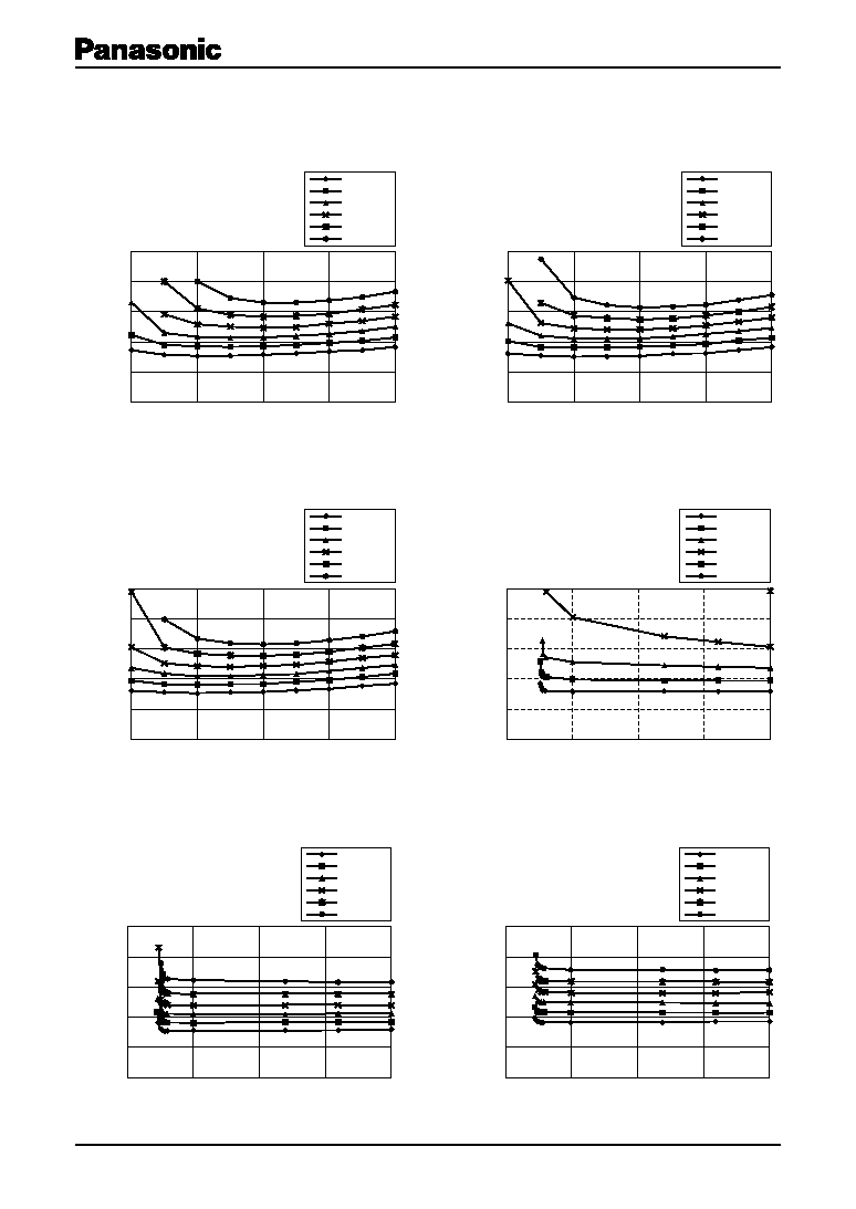
Technical Data (continued)
· Output Rise Time
5
DN8798MS
SPC00008CJB
I
O
= 10 mA
I
O
= 9 mA
I
O
= 8 mA
I
O
= 7 mA
I
O
= 6 mA
I
O
= 5 mA
Output Low voltage (V)
0.25
0.20
0.15
0.10
0.05
0
-50
0
50
100
150
Ambient temperature (
°C)
I
O
= 10 mA
I
O
= 9 mA
I
O
= 8 mA
I
O
= 7mA
I
O
= 6 mA
I
O
= 5 mA
Output Low voltage (V)
0.25
0.20
0.15
0.10
0.05
0
-50
0
50
100
150
Ambient temperature (
°C)
I
O
= 10 mA
I
O
= 9 mA
I
O
= 8 mA
I
O
= 7 mA
I
O
= 6 mA
I
O
= 5 mA
Output Low voltage (V)
0.25
0.20
0.15
0.10
0.05
0
-50
0
50
100
150
Ambient temperature (
°C)
I
O
= 10 mA
I
O
= 9 mA
I
O
= 8 mA
I
O
= 7 mA
I
O
= 6 mA
I
O
= 5 mA
Output Low voltage (V)
0.25
0.20
0.15
0.10
0.05
0
0
5
10
15
20
Supply voltage (V)
I
O
= 10 mA
I
O
= 9 mA
I
O
= 8 mA
I
O
= 7 mA
I
O
= 6 mA
I
O
= 5 mA
Output Low voltage (V)
0.25
0.20
0.15
0.10
0.05
0
0
5
10
15
20
Supply voltage (V)
I
O
= 10 mA
I
O
= 9 mA
I
O
= 8 mA
I
O
= 7 mA
I
O
= 6 mA
I
O
= 5 mA
Output Low voltage (V)
0.25
0.20
0.15
0.10
0.05
0
0
5
10
15
20
Supply voltage (V)
Technical Data (continued)
· Main characterisitcs
Output low voltage
Ambient temperature (V
CC
= 2.7 V)
Output low voltage
Ambient temperature (V
CC
= 5.0 V)
Output low voltage
Ambient temperature (V
CC
= 20 V)
Output low voltage
Supply voltage (Temp. = -50°C)
Output low voltage
Supply voltage (Temp. = 25°C)
Output low voltage
Supply voltage (Temp. = 150°C)
Document Outline