©
Semiconductor Components Industries, LLC, 2002
June, 2002 ≠ Rev. 5
1
Publication Order Number:
1N6267A/D
1N6267A Series
1500 Watt Mosorb
TM
Zener
Transient Voltage
Suppressors
Unidirectional*
Mosorb devices are designed to protect voltage sensitive
components from high voltage, high≠energy transients. They have
excellent clamping capability, high surge capability, low zener
i m p e d a n c e a n d f a s t r e s p o n s e t i m e . T h e s e d e v i c e s a r e
ON Semiconductor's exclusive, cost-effective, highly reliable
Surmetic
TM
axial leaded package and are ideally-suited for use in
communication systems, numerical controls, process controls,
medical equipment, business machines, power supplies and many
other industrial/consumer applications, to protect CMOS, MOS and
Bipolar integrated circuits.
Specification Features:
∑
Working Peak Reverse Voltage Range ≠ 5.8 V to 214 V
∑
Peak Power ≠ 1500 Watts @ 1 ms
∑
ESD Rating of Class 3 (>16 KV) per Human Body Model
∑
Maximum Clamp Voltage @ Peak Pulse Current
∑
Low Leakage < 5
mA Above 10 V
∑
UL 497B for Isolated Loop Circuit Protection
∑
Response Time is Typically < 1 ns
Mechanical Characteristics:
CASE:
Void-free, transfer-molded, thermosetting plastic
FINISH:
All external surfaces are corrosion resistant and leads are
readily solderable
MAXIMUM LEAD TEMPERATURE FOR SOLDERING PURPOSES:
230
∞
C, 1/16
from the case for 10 seconds
POLARITY:
Cathode indicated by polarity band
MOUNTING POSITION:
Any
MAXIMUM RATINGS
Rating
Symbol
Value
Unit
Peak Power Dissipation (Note 1)
@ T
L
25
∞
C
P
PK
1500
Watts
Steady State Power Dissipation
@ T
L
75
∞
C, Lead Length = 3/8
Derated above T
L
= 75
∞
C
P
D
5.0
20
Watts
mW/
∞
C
Thermal Resistance, Junction≠to≠Lead
R
q
JL
20
∞
C/W
Forward Surge Current (Note 2)
@ T
A
= 25
∞
C
I
FSM
200
Amps
Operating and Storage
Temperature Range
T
J
, T
stg
≠ 65 to
+175
∞
C
1. Nonrepetitive current pulse per Figure 5 and derated above T
A
= 25
∞
C per
Figure 2.
2. 1/2 sine wave (or equivalent square wave), PW = 8.3 ms, duty cycle = 4 pulses
per minute maximum.
*Please see 1.5KE6.8CA to 1.5KE250CA for Bidirectional Devices
Devices listed in
bold, italic are ON Semiconductor
Preferred devices. Preferred devices are recommended
choices for future use and best overall value.
AXIAL LEAD
CASE 41A
PLASTIC
L = Assembly Location
1N6xxxA = JEDEC Device Code
1.5KExxxA = ON Device Code
YY = Year
WW = Work Week
Cathode
Anode
Device
Package
Shipping
ORDERING INFORMATION
1.5KExxxA
Axial Lead
500 Units/Box
1.5KExxxARL4
Axial Lead
1500/Tape & Reel
1N6xxxA
Axial Lead
500 Units/Box
1N6xxxARL4*
Axial Lead
1500/Tape & Reel
L
1N6
xxxA
1.5KE
xxxA
YYWW
http://onsemi.com
*1N6302A Not Available in 1500/Tape & Reel

Uni≠Directional TVS
I
PP
I
F
V
I
I
R
I
T
V
RWM
V
C
V
BR
V
F
1N6267A Series
http://onsemi.com
2
ELECTRICAL CHARACTERISTICS
(T
A
= 25
∞
C unless
otherwise noted, V
F
= 3.5 V Max., I
F
(Note 3) = 100 A)
Symbol
Parameter
I
PP
Maximum Reverse Peak Pulse Current
V
C
Clamping Voltage @ I
PP
V
RWM
Working Peak Reverse Voltage
I
R
Maximum Reverse Leakage Current @ V
RWM
V
BR
Breakdown Voltage @ I
T
I
T
Test Current
Q
V
BR
Maximum Temperature Coefficient of V
BR
I
F
Forward Current
V
F
Forward Voltage @ I
F

1N6267A Series
http://onsemi.com
3
ELECTRICAL CHARACTERISTICS
(T
A
= 25
∞
C unless otherwise noted, V
F
= 3.5 V Max. @ I
F
(Note 3)
= 100 A)
V
RWM
Breakdown Voltage
V
C
@ I
PP
(Note 7)
JEDEC
Device
V
RWM
(Note 5)
I
R
@ V
RWM
V
BR
(Note 6) (Volts)
@ I
T
V
C
I
PP
Q
V
BR
Device
Device
(Note 4)
(Volts)
(
m
A)
Min
Nom
Max
(mA)
(Volts)
(A)
(%/
∞
C)
1.5KE6.8A
1N6267A
5.8
1000
6.45
6.8
7.14
10
10.5
143
0.057
1.5KE7.5A
1N6268A
6.4
500
7.13
7.5
7.88
10
11.3
132
0.061
1.5KE8.2A
1N6269A
7.02
200
7.79
8.2
8.61
10
12.1
124
0.065
1.5KE9.1A
1N6270A
7.78
50
8.65
9.1
9.55
1
13.4
112
0.068
1.5KE10A
1N6271A
8.55
10
9.5
10
10.5
1
14.5
103
0.073
1.5KE11A
1N6272A
9.4
5
10.5
11
11.6
1
15.6
96
0.075
1.5KE12A
1N6273A
10.2
5
11.4
12
12.6
1
16.7
90
0.078
1.5KE13A
1N6274A
11.1
5
12.4
13
13.7
1
18.2
82
0.081
1.5KE15A
1N6275A
12.8
5
14.3
15
15.8
1
21.2
71
0.084
1.5KE16A
1N6276A
13.6
5
15.2
16
16.8
1
22.5
67
0.086
1.5KE18A
1N6277A
15.3
5
17.1
18
18.9
1
25.2
59.5
0.088
1.5KE20A
1N6278A
17.1
5
19
20
21
1
27.7
54
0.09
1.5KE22A
1N6279A
18.8
5
20.9
22
23.1
1
30.6
49
0.092
1.5KE24A
1N6280A
20.5
5
22.8
24
25.2
1
33.2
45
0.094
1.5KE27A
1N6281A
23.1
5
25.7
27
28.4
1
37.5
40
0.096
1.5KE30A
1N6282A
25.6
5
28.5
30
31.5
1
41.4
36
0.097
1.5KE33A
1N6283A
28.2
5
31.4
33
34.7
1
45.7
33
0.098
1.5KE36A
1N6284A
30.8
5
34.2
36
37.8
1
49.9
30
0.099
1.5KE39A
1N6285A
33.3
5
37.1
39
41
1
53.9
28
0.1
1.5KE43A
1N6286A
36.8
5
40.9
43
45.2
1
59.3
25.3
0.101
1.5KE47A
1N6287A
40.2
5
44.7
47
49.4
1
64.8
23.2
0.101
1.5KE51A
1N6288A
43.6
5
48.5
51
53.6
1
70.1
21.4
0.102
1.5KE56A
1N6289
47.8
5
53.2
56
58.8
1
77
19.5
0.103
1.5KE62A
1N6290A
53
5
58.9
62
65.1
1
85
17.7
0.104
1.5KE68A
1N6291A
58.1
5
64.6
68
71.4
1
92
16.3
0.104
1.5KE75A
1N6292A
64.1
5
71.3
75
78.8
1
103
14.6
0.105
1.5KE82A
1N6293A
70.1
5
77.9
82
86.1
1
113
13.3
0.105
1.5KE91A
1N6294A
77.8
5
86.5
91
95.5
1
125
12
0.106
1.5KE100A
1N6295A
85.5
5
95
100
105
1
137
11
0.106
1.5KE110A
1N6296A
94
5
105
110
116
1
152
9.9
0.107
1.5KE120A
1N6297A
102
5
114
120
126
1
165
9.1
0.107
1.5KE130A
1N6298A
111
5
124
130
137
1
179
8.4
0.107
1.5KE150A
1N6299A
128
5
143
150
158
1
207
7.2
0.108
1.5KE160A
1N6300A
136
5
152
160
168
1
219
6.8
0.108
1.5KE170A
1N6301A
145
5
162
170
179
1
234
6.4
0.108
1.5KE180A
1N6302A*
154
5
171
180
189
1
246
6.1
0.108
1.5KE200A
1N6303A
171
5
190
200
210
1
274
5.5
0.108
1.5KE220A
185
5
209
220
231
1
328
4.6
0.109
1.5KE250A
214
5
237
250
263
1
344
5
0.109
3. 1/2 sine wave (or equivalent square wave), PW = 8.3 ms, duty cycle = 4 pulses per minute maximum.
4. Indicates JEDEC registered data
5. A transient suppressor is normally selected according to the maximum working peak reverse voltage (V
RWM
), which should be equal to or
greater than the dc or continuous peak operating voltage level.
6. V
BR
measured at pulse test current I
T
at an ambient temperature of 25
∞
C
7. Surge current waveform per Figure 5 and derate per Figures 1 and 2.
*Not Available in the 1500/Tape & Reel

1N6267A Series
http://onsemi.com
4
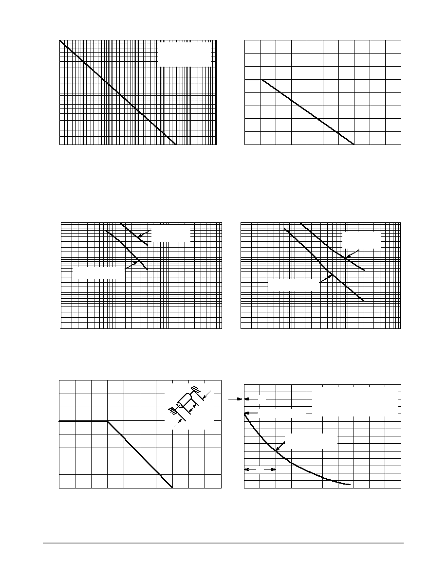
Figure 1. Pulse Rating Curve
100
80
60
40
20
0
0
25
50
75
100 125 150 175
200
PEAK PULSE DERA
TING IN % OF
PEAK POWER OR CURRENT
@
T A
= 25
C
∞
T
A
, AMBIENT TEMPERATURE (
∞
C)
Figure 2. Pulse Derating Curve
5
4
3
2
1
25
50
75
100
125
150
175
200
P D
, STEADY
ST
A
TE POWER DISSIP
A
TION (W
A
TTS)
T
L
, LEAD TEMPERATURE (
∞
C)
3/8
3/8
0
0
100
50
0
0
1
2
3
4
t, TIME (ms)
, V
ALUE (%)
t
r
t
P
PEAK VALUE - I
PP
HALF VALUE -
I
PP
2
PULSE WIDTH (t
P
) IS DEFINED AS
THAT POINT WHERE THE PEAK
CURRENT DECAYS TO 50% OF I
PP
.
tr
10 ms
1 ms
10 ms
100 ms
1 ms
10 ms
100
10
1
t
P
, PULSE WIDTH
P PK
, PEAK POWER (kW)
NONREPETITIVE
PULSE WAVEFORM
SHOWN IN FIGURE 5
0.1 ms
I PP
Figure 3. Capacitance versus Breakdown Voltage
1N6267A/1.5KE6.8A
through
1N6303A/1.5KE200A
V
BR
, BREAKDOWN VOLTAGE (VOLTS)
1
10
100
1000
10,000
1000
100
10
C, CAP
ACIT
ANCE (pF)
MEASURED @ V
RWM
MEASURED @
ZERO BIAS
Figure 4. Steady State Power Derating
Figure 5. Pulse Waveform
1N6373, ICTE-5, MPTE-5,
through
1N6389, ICTE-45, C, MPTE-45, C
V
BR
, BREAKDOWN VOLTAGE (VOLTS)
1
10
100
1000
10,000
1000
100
10
C, CAP
ACIT
ANCE (pF)
MEASURED @
ZERO BIAS
MEASURED @ V
RWM

1N6267A Series
http://onsemi.com
5
1N6373, ICTE-5, MPTE-5,
through
1N6389, ICTE-45, C, MPTE-45, C
1.5KE6.8CA
through
1.5KE200CA
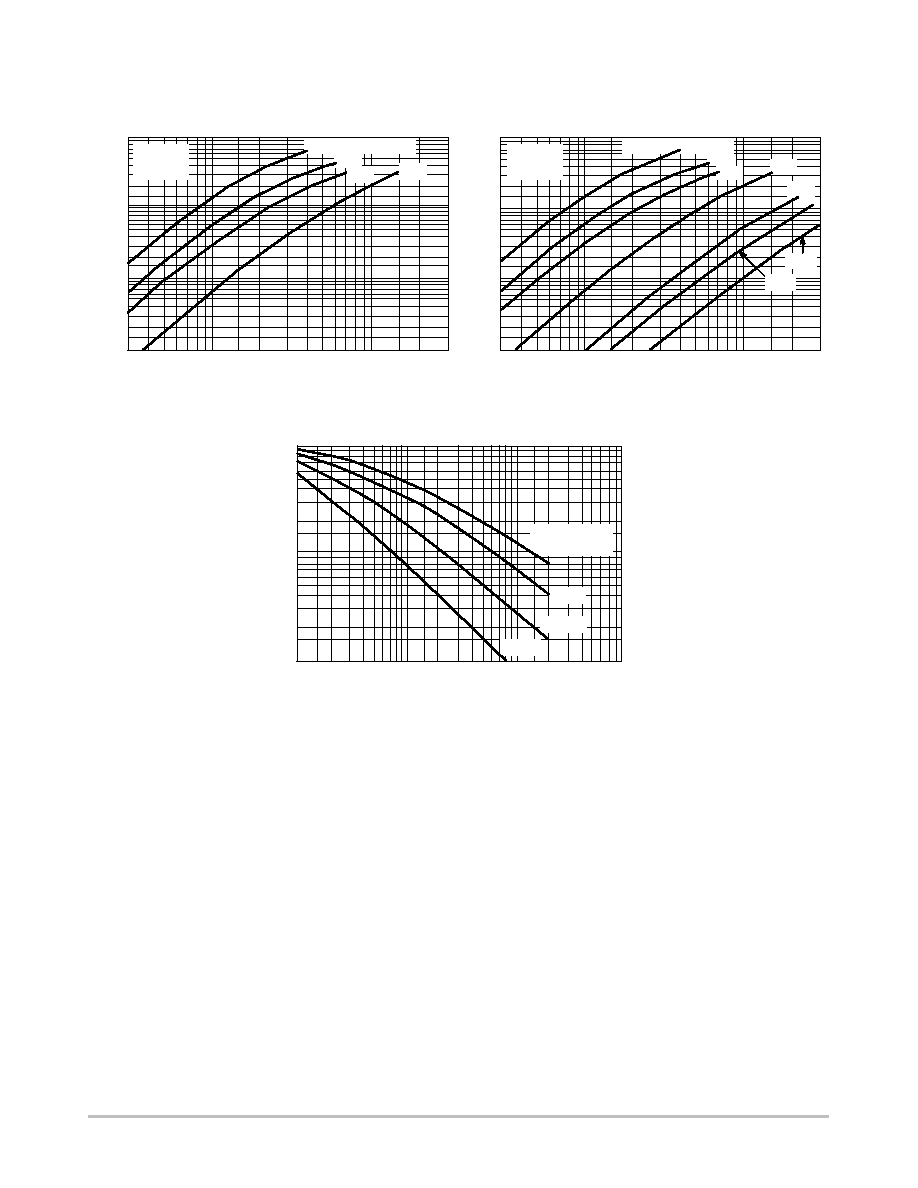
Figure 6. Dynamic Impedance
1000
500
200
100
50
20
10
5
2
1
1000
500
200
100
50
20
10
5
2
1
0.3
0.5 0.7 1
2
3
5
7 10
20 30
DV
BR
, INSTANTANEOUS INCREASE IN V
BR
ABOVE V
BR(NOM)
(VOLTS)
0.3
0.5 0.7 1
2
3
5
7 10
20 30
DV
BR
, INSTANTANEOUS INCREASE IN V
BR
ABOVE V
BR(NOM)
(VOLTS)
I T
,
TEST
CURRENT
(AMPS)
V
BR(NOM)
= 6.8 to 13 V
T
L
= 25
∞
C
t
P
= 10 ms
V
BR(NOM)
= 6.8 to 13 V
20 V
24 V
43 V
75 V
180 V
120 V
20 V
24 V
43 V
Figure 7. Typical Derating Factor for Duty Cycle
DERA
TING F
ACT
OR
1 ms
10 ms
1
0.7
0.5
0.3
0.05
0.1
0.2
0.01
0.02
0.03
0.07
100 ms
0.1
0.2
0.5
2
5
10
50
1
20
100
D, DUTY CYCLE (%)
PULSE WIDTH
10 ms
T
L
= 25
∞
C
t
P
= 10 ms
I T
,
TEST
CURRENT
(AMPS)
APPLICATION NOTES
RESPONSE TIME
In most applications, the transient suppressor device is
placed in parallel with the equipment or component to be
protected. In this situation, there is a time delay associated
with the capacitance of the device and an overshoot
condition associated with the inductance of the device and
the inductance of the connection method. The capacitance
effect is of minor importance in the parallel protection
scheme because it only produces a time delay in the
transition from the operating voltage to the clamp voltage as
shown in Figure 8.
The inductive effects in the device are due to actual
turn-on time (time required for the device to go from zero
current to full current) and lead inductance. This inductive
effect produces an overshoot in the voltage across the
equipment or component being protected as shown in
Figure 9. Minimizing this overshoot is very important in the
application, since the main purpose for adding a transient
suppressor is to clamp voltage spikes. These devices have
excellent response time, typically in the picosecond range
and negligible inductance. However, external inductive
effects could produce unacceptable overshoot. Proper
circuit layout, minimum lead lengths and placing the
suppressor device as close as possible to the equipment or
components to be protected will minimize this overshoot.
Some input impedance represented by Z
in
is essential to
prevent overstress of the protection device. This impedance
should be as high as possible, without restricting the circuit
operation.
DUTY CYCLE DERATING
The data of Figure 1 applies for non-repetitive conditions
and at a lead temperature of 25
∞
C. If the duty cycle increases,
the peak power must be reduced as indicated by the curves
of Figure 7. Average power must be derated as the lead or


