1/20
° Semiconductor
MSM80C48/49/50, MSM80C35/39/40
° Semiconductor
MSM80C48/49/50
MSM80C35/39/40
CMOS 8-Bit Microcontroller
GENERAL DESCRIPTION
The OKI MSM80C48/MSM80C49/MSM80C50 are 8-bit, low-power, high-performance micro-
controllers implemented in silicon-gate complementary metal-oxide semiconductor technology.
Integrated within these chips are 8K/16K/32K bits of mask program ROM, 512/1024/2048 bits
of data RAM, 27 I/O lines, built-in 8 bit timer/counter, and oscillator. Program memory and data
paths are byte wide. Eleven new instructions have been added to the NMOS version's instruction
set, thereby optimizing power down, port data transfer, decrement and port float functions.
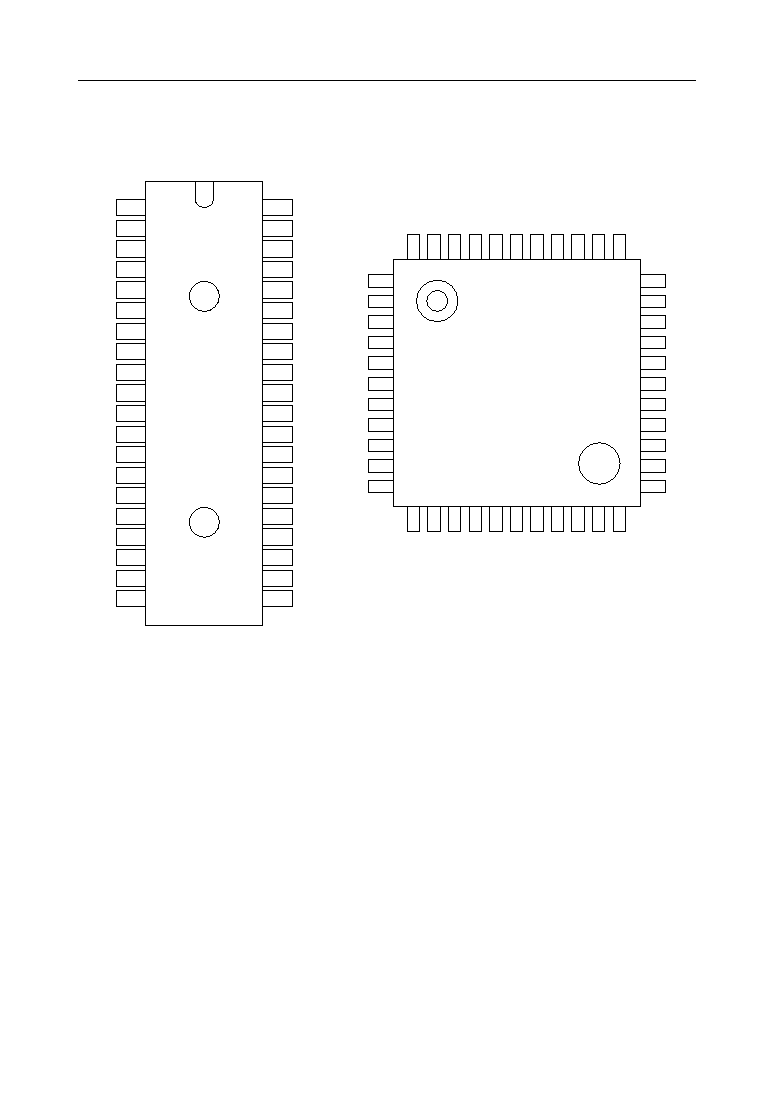
Available in 40-pin plastic DIP (RS) or 44-pin plastic flat packages QFP (GSK).
FEATURES
∑ Lower power consumption enabled by CMOS silicon gate process
∑ Completely static operation
∑ Improved power-down feature
∑ Instruction cycle
: 1.36 ms (11 MHz) V
CC
=4.5 to 6.0 V (MSM80C48/49)
2.5 ms (6 MHz) V
CC
=3.5 to 6.0 V (MSM80C50)
∑ 111 instructions
∑ All instructions are usable even during execution of external ROM instructions.
∑ Operation facility
Addition, logical operations, and decimal adjust
∑ Program memory (ROM)
: 1K words • 8 bits (MSM80C48)
: 2K words • 8 bits (MSM80C49)
: 4K words • 8 bits (MSM80C50)
∑ Data memory (RAM)
: 64 words • 8 bits (MSM80C48)
: 128 words • 8 bits (MSM80C49)
: 256 words • 8 bits (MSM80C50)
∑ Two sets of working registers
∑ External and timer interrupts
∑ Two test inputs
∑ Built-in 8-bit timer counter
∑ Extendable external memory and I/O ports
∑ I/O port
Input-output port
: 2 ports • 8 bits
Data bus input-output port
: 1 port • 8 bits
∑ Single-step execution function
∑ Wide range of operating voltage, from + 2.5 V to + 6 V of V
CC
∑ High noise margin action
∑ Compatible with Intel's 8048, 8049 and 8050
∑ Package
40-pin plastic DIP (DIP40-P-600-2.54)
:
(MSM80C48-•••RS)
(MSM80C49-•••RS)
(MSM80C50-•••RS)
(MSM80C35RS)
(MSM80C39RS)
(MSM80C40RS)
44-pin plastic QFP(QFP44-P-910-0.80-2K) :
(MSM80C48-•••GS-2K)
(MSM80C49-•••GS-2K)
(MSM80C50-•••GS-2K)
(MSM80C35GS-2K)
(MSM80C39GS-2K)
(MSM80C40GS-2K)
••• indicates the code number.
E2E1022-27-Y4
This version: Jan. 1998
Previous version: Nov. 1996
4/20
° Semiconductor
MSM80C48/49/50, MSM80C35/39/40
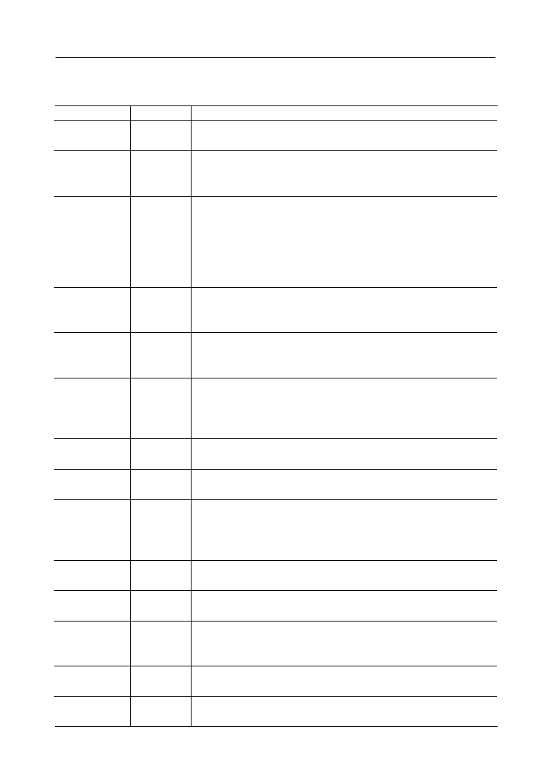
PIN DESCRIPTIONS
Symbol
Type
Description
P1
0
-P1
7
(PORT 1)
8-bit quasi-bidirectional port
I/O
P2
0
-P2
7
(PORT 2)
8-bit quasi-bidirectional port
The high-order four bits of external program memory addresses can be output
from P2.0-P2.3, to which the I/O expander MSM82C43RS may also be connected.
I/O
DB
0
-DB
7
(BUS)
Bidirectional port
The low-order eight bits of external program memory address can be output
from this port, and the addressed instruction is fetched under the control of
PSEN signal. Also, the external data memory address is output, and data is
read and written synchronously using RD and WR signals.
The port can also serve as either a statically latched output port or a
non-latching input port.
I/O
T0
(Test 0)
The input can be tested with the conditional jump instructions JT0 and JNT0.
The execution of the ENT0 CLK instruction causes a clock output.
I/O
T1
(Test 1)
The input can be tested with the conditional jump instructions JT1 and JNT1.
The execution of a STRT CNT instruction causes an internal counter input.
I
INT
(Interrupt)
Interrupt input. If interrupt is enabled, INT input initiates an interrupt.
Interrupt is disabled after a reset.
Also testable with a JNI instruction. Can be used to terminate the power-down
mode. (Active "0" level)
I
RD
(Read)
A signal to read data from external data memory. (Active "0" level)
O
WR
(Write)
A signal to write data to external data memory. (Active "0" level)
O
ALE
Address &
Data Latch
Clock
This signal is generated in each cycle. It may be used as a clock output.
External data memory or external program memory is addressed upon the
falling edge. For the external ROM, this signal is used to latch the bus port data
upon the ALE signal rise-up after the execution of the OUTL BUS, A instruction.
O
PSEN Program
Store Enable
A signal to fetch an instruction from external program memory
(Active "0" level)
O
RESET
RESET input initialize the processor. (Active "0" level)
Used to terminate the power-down mode.
I
SS
(Single Step)
A program is executed step by step. This pin can also be used to control
internal oscillation when the power-down mode is reset.
(Active "0" level)
I
EA
(External Access)
When held at high level, all instructions are fetched from external memory.
(Active "1" level)
I
PROG
(Expander Strobe)
This output strobes the MSM82C43RS I/O expander.
O
5/20
° Semiconductor
MSM80C48/49/50, MSM80C35/39/40
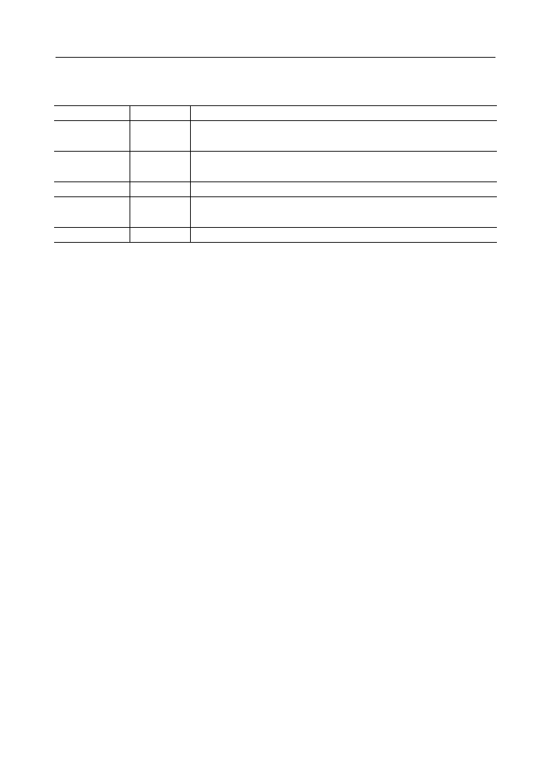
PIN DESCRIPTIONS (Continued)
Note: A minimum of two machine cycles are required in RESET pulse duration under the
specified power supply and stable oscillator frequency.
Symbol
Type
Description
XTAL1
(Crystal 1)
One side of the internal crystal oscillator. An external clock can also be input.
I
XTAL2
(Crystal 2)
Other side of the internal crystal oscillator.
O
V
CC
Power supply pin
--
V
DD
Standby control input. Normally, "1" level. When set to "0" level, oscillation is
stopped and prosessor goes into standby mode.
--
V
SS
GND
--