 | –≠–ª–µ–∫—Ç—Ä–æ–Ω–Ω—ã–π –∫–æ–º–ø–æ–Ω–µ–Ω—Ç: 30141-23 | –°–∫–∞—á–∞—Ç—å:  PDF PDF  ZIP ZIP |
Document Outline
- List of Figures
- List of Tables
- Table 2-1.� Pin Type Definitions
- Table 2-2.� 352 BGA Pin Assignments - Sorted by Pin Number
- Table 2-3.� 352 BGA Pin Assignments - Sorted Alphabetically by Signal Name
- Table 2-4.� 320 SPGA Pin Assignments - Sorted by Pin Number
- Table 2-5.� 320 SPGA Pin Assignments - Sorted Alphabetically by Signal Name
- Table 3-1.� Initialized Core Register Controls �
- Table 3-2.� Application Register Set
- Table 3-3.� Segment Register Selection Rules
- Table 3-4.� EFLAGS Register
- Table 3-5.� System Register Set
- Table 3-6.� Control Registers Map
- Table 3-7.� CR4-CR0 Bit Definitions �
- Table 3-8.� Effects of Various Combinations of EM, TS, and MP Bits
- Table 3-9.� Configuration Register Summary
- Table 3-10.� Configuration Register Map
- Table 3-11.� Configuration Registers �
- Table 3-12.� Debug Registers
- Table 3-13.� DR7 and DR6 Bit Definitions
- Table 3-14.� TLB Test Registers
- Table 3-15.� TR7-TR6 Bit Definitions �
- Table 3-16.� Cache Test Registers
- Table 3-17.� TR5-TR3 Bit Definitions
- Table 3-18.� Cache Test Operations
- Table 3-19.� Memory Addressing Modes
- Table 3-20.� GDTR, LDTR and IDTR Registers
- Table 3-21.� Application and System Segment Descriptors
- Table 3-22.� Application and System Segment Descriptors Bit Definitions �
- Table 3-23.� Application and System Segment Descriptors TYPE Bit Definitions �
- Table 3-24.� Gate Descriptors
- Table 3-25.� Gate Descriptors Bit Definitions
- Table 3-26.� 32-Bit Task State Segment (TSS) Table
- Table 3-27.� 16-Bit Task State Segment (TSS) Table
- Table 3-28.� Directory Table Entry (DTE) and Page Table Entry (PTE)
- Table 3-29.� Interrupt Vector Assignments
- Table 3-30.� Interrupt and Exception Priorities
- Table 3-31.� Exception Changes in Real Mode
- Table 3-32.� Error Codes
- Table 3-33.� Error Code Bit Definitions
- Table 3-34.� SMI# and SMINT Recognition Requirements
- Table 3-35.� SMM Memory Space Header
- Table 3-36.� SMM Memory Space Header Description
- Table 3-37.� SMM Instruction Set
- Table 3-38.� Descriptor Types Used for Control Transfer
- Table 3-39.� FPU Registers
- Table 4-1.� GCR Register
- Table 4-2.� Display Resolution Skip Counts
- Table 4-3.� L1 Cache BitBLT Register Summary
- Table 4-4.� L1 Cache BitBLT Registers
- Table 4-5.� Scratchpad Organization
- Table 4-6.� Display Driver Instructions
- Table 4-7.� CPU-Access Instructions
- Table 4-8.� Address Map for CPU-Access Registers
- Table 4-9.� Internal Bus Interface Unit Register Summary
- Table 4-10.� Internal Bus Interface Unit Registers�
- Table 4-11.� Region-Control-Field Bit Definitions
- Table 4-12.� Synchronous DRAM Configurations
- Table 4-13.� Basic Command Truth Table
- Table 4-14.� Address Line Programming during MRS Cycles
- Table 4-15.� Memory Controller Register Summary
- Table 4-16.� Memory Controller Registers �
- Table 4-17.� Auto LOI -- 2 DIMMs, Same Size, 1 DIMM Bank
- Table 4-18.� Auto LOI -- 2 DIMMs, Same Size, 2 DIMM Banks
- Table 4-19.� Non-Auto LOI -- 1 or 2 DIMMs, Different Sizes, 1 DIMM Bank
- Table 4-20.� Non-Auto LOI -- 1 or 2 DIMMs, Different Sizes, 2 DIMM Banks
- Table 4-21.� Graphics Pipeline Registers
- Table 4-22.� GP_RASTER_MODE Bit Patterns
- Table 4-23.� Common Raster Operations
- Table 4-24.� Graphics Pipeline Configuration Register Summary �
- Table 4-25.� Graphics Pipeline Configuration Registers �
- Table 4-26.� TFT Panel Display Modes
- Table 4-27.� TFT Panel Data Bus Formats
- Table 4-28.� CRT Display Modes
- Table 4-29.� Display Controller Register Summary �
- Table 4-30.� Display Controller Configuration and Status Registers �
- Table 4-31.� Display Controller Memory Organization Registers �
- Table 4-32.� Display Controller Timing Registers �
- Table 4-33.� Display Controller Cursor Position Registers �
- Table 4-34.� Display Controller Color Registers
- Table 4-35.� Display Controller Palette and RAM Diagnostic Registers�
- Table 4-36.� Special-Cycle Code to CONFIG_ADDRESS
- Table 4-37.� PCI Configuration Registers
- Table 4-38.� Format for Accessing the Internal PCI Configuration Registers
- Table 4-39.� PCI Configuration Space Register Summary
- Table 4-40.� PCI Configuration Registers �
- Table 5-1.� Standard VGA Modes
- Table 5-2.� VGA Configuration Registers Summary
- Table 5-3.� VGA Configuration Registers
- Table 5-4.� Virtual VGA Register Summary
- Table 5-5.� Virtual VGA Registers
- Table 6-1.� Power Management Register Summary �
- Table 6-2.� Power Management Control and Status Registers �
- Table 6-3.� Power Management Programmable Address Region Registers
- Table 7-1.� Part Numbers
- Table 7-2.� Pins with 20-kohm Internal Resistor
- Table 7-3.� Absolute Maximum Ratings
- Table 7-4.� Operating Conditions
- Table 7-5.� DC Characteristics
- Table 7-6.� Drive Level and Measurement Points for Switching Characteristics
- Table 7-7.� Clock Signals
- Table 7-8.� System Signals
- Table 7-9.� PCI Interface Signals
- Table 7-10.� SDRAM Interface Signals
- Table 7-11.� Video Interface Signals
- Table 7-12.� JTAG AC Specification
- Table 8-1.� Junction-to-Case Thermal Resistance for SPGA and BGA Packages
- Table 8-2.� Case-to-Ambient Thermal Resistance Examples @ 85�C
- Table 8-3.� Mechanical Package Outline Legend
- Table 9-1.� General Instruction Set Format
- Table 9-2.� Instruction Fields
- Table 9-3.� Instruction Prefix Summary
- Table 9-4.� w Field Encoding
- Table 9-5.� d Field Encoding
- Table 9-6.� s Field Encoding
- Table 9-7.� eee Field Encoding
- Table 9-8.� General Registers Selected by mod r/m Fields and w Field
- Table 9-9.� mod r/m Field Encoding
- Table 9-10.� General Registers Selected by reg Field
- Table 9-11.� sreg2 Field Encoding
- Table 9-12.� sreg3 Field Encoding
- Table 9-13.� ss Field Encoding
- Table 9-14.� index Field Encoding
- Table 9-15.� mod base Field Encoding
- Table 9-16.� CPUID Levels Summary
- Table 9-17.� CPUID Data Returned when EAX = 0
- Table 9-18.� EAX, EBX, ECX CPUID Data Returned when EAX = 1
- Table 9-19.� EDX CPUID Data Returned when EAX = 1�
- Table 9-20.� Standard CPUID with EAX = 00000002h
- Table 9-21.� Maximum Extended CPUID Level
- Table 9-22.� EAX, EBX, ECX CPUID Data Returned when EAX = 80000001h
- Table 9-23.� EDX CPUID Data Returned when EAX = 80000001h
- Table 9-24.� Official CPU Name
- Table 9-25.� Standard CPUID with EAX = 80000005h
- Table 9-26.� Processor Core Instruction Set Table Legend
- Table 9-27.� Processor Core Instruction Set Summary �
- Table 9-28.� FPU Instruction Set Table Legend
- Table 9-29.� FPU Instruction Set Summary �
- Table 9-30.� MMX Instruction Set Table Legend
- Table 9-31.� MMX Instruction Set Summary �
- Table 9-32.� Extend MMX Instruction Set Table Legend
- Table 9-33.� Extended MMX Instruction Set Summary �
- Table A-1.� Revision History
- Table A-2.� Edits to Current Revision
- 1.0 Architecture Overview
- 2.0 Signal Definitions
- 3.0 Processor Programming
- 4.0 Integrated Functions
- 5.0 Virtual Subsystem Architecture
- 6.0 Power Management
- 7.0 Electrical Specifications
- 8.0 Package Specifications
- 9.0 Instruction Set
- Appendix A Support Documentation
© 2000 National Semiconductor Corporation
www.national.com
GeodeTM
G
Xm
P
r
ocessor
I
ntegrated
x
86
S
o
l
u
t
i
o
n
with
M
M
X
Suppor
t
April 2000
GeodeTM GXm Processor
Integrated x86 Solution with MMX Support
General Description
The National Semiconductor
Æ
GeodeTM GXm processor
is an advanced 32-bit x86 compatible processor offering
high performance, fully accelerated 2D graphics, a 64-bit
synchronous DRAM controller and a PCI bus controller,
all on a single chip that is compatible with Intel's MMX
technology.
The GXm processor core is a proven design that offers
competitive CPU performance. It has integer and floating
point execution units that are based on sixth-generation
technology. The integer core contains a single, six-stage
execution pipeline and offers advanced features such as
operand forwarding, branch target buffers, and extensive
write buffering. A 16 KB write-back L1 cache is accessed
in a unique fashion that eliminates pipeline stalls to fetch
operands that hit in the cache.
In addition to the advanced CPU features, the GXm pro-
cessor integrates a host of functions which are typically
implemented with external components. A full-function
graphics accelerator provides pixel processing and ren-
dering functions.
A separate on-chip video buffer enables >30 fps MPEG1
video playback when used together with the CS5530 I/O
companion chip. Graphics and system memory accesses
are supported by a tightly-coupled synchronous DRAM
(SDRAM) memory controller. This tightly coupled memory
subsystem eliminates the need for an external L2 cache.
The GXm processor includes Virtual System Architec-
ture
Æ
(VSATM technology) enabling XpressGRAPHICS
and XpressAUDIO subsystems as well as generic emula-
tion capabilities. Software handler routines for the Xpress-
GRAPHICS and XpressAUDIO subsystems can be
included in the BIOS and provide compatible VGA and 16-
bit industry standard audio emulation. XpressAUDIO tech-
nology eliminates much of the hardware traditionally asso-
ciated with audio functions.
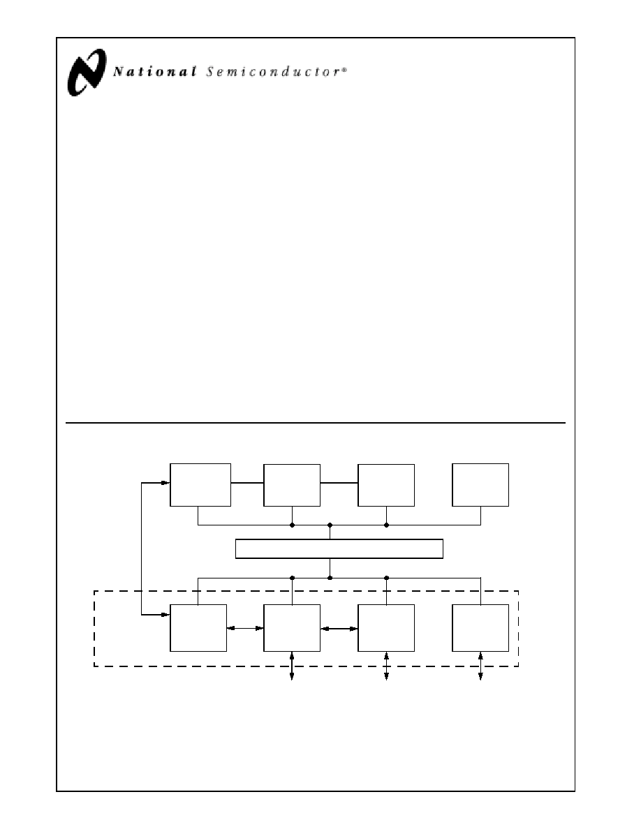
GeodeTM GXm Processor Internal Block Diagram
Write-Back
Unit
FPU
Internal Bus Interface Unit
Graphics
Memory
Display
PCI
SDRAM Port
CS5530
PCI Bus
Integer
Cache Unit
Integrated
Functions
MMU
(CRT/LCD TFT)
X-Bus
Pipeline
Controller
Controller
Controller
C-Bus
National Semiconductor and Virtual System Architecture are registered trademarks of National Semiconductor Corporation.
Geode and VSA are trademarks of National Semiconductor Corporation.
For a complete listing of National Semiconductor trademarks, please visit www.national.com/trademarks.

www.national.com
2
Revision 3.1
GeodeTM
G
Xm
Pr
ocessor
Features
General Features
Packaged in:
-- 352-Terminal Ball Grid Array (BGA) or
-- 320-Pin Staggered Pin Grid Array (SPGA)
0.35-micron four layer metal CMOS process
Split rail design (3.3V I/O and 2.9V core)
32-Bit x86 Processor
Supports the MMX instruction set extension for the
acceleration of multimedia applications
Speeds offered up to 266 MHz
16 KB unified L1 cache
Integrated Floating Point Unit (FPU)
Re-entrant System Management Mode (SMM)
enhanced for VSA
PCI Controller
Fixed, rotating, hybrid, or ping-pong arbitration
Supports up to three PCI bus masters
Synchronous CPU and PCI bus clock frequency
Supports concurrency between PCI master and L1
cache
Power Management
Designed to support CS5530 power management
architecture
CPU only Suspend or full 3V Suspend supported:
-- Clocks to CPU core stopped for CPU Suspend
-- All on-chip clocks stopped for 3V Suspend
-- Suspend refresh supported for 3V Suspend
Virtual Systems Architecture Technology
Architecture allows OS independent (software) virtual-
ization of hardware functions
Provides compatible high performance legacy VGA
core functionality
Note: GUI (Graphical User Interface) graphics accel-
eration is pure hardware.
Provides 16-bit XpressAUDIO subsystem
2D Graphics Accelerator
Graphics pipeline performance significantly increased
over previous generations by pipelining burst
reads/writes
Accelerates BitBLTs, line draw, text
Supports all 256 raster operations
Supports transparent BLTs
Runs at core clock frequency
Full VGA and VESA mode support
Special "Driver level" instructions utilize internal
scratchpad for enhanced performance
Display Controller
Video Generator (VG) improves memory efficiency for
display refresh with SDRAM
Supports a separate MPEG1 video buffer and data
path to enable video acceleration in the CS5530
Internal palette RAM for use with the CS5530
Direct interface to CS5530 for CRT and TFT flat panel
support which eliminates need for external RAMDAC
Hardware frame buffer compressor/decompressor
Hardware cursor
Supports up to 1280x1024x8 bpp and 1024x768x16
bpp
XpressRAM Subsystem
Memory control/interface directly from CPU
64-Bit wide memory bus
Support for:
-- Two 168-pin unbuffered DIMMs
-- Up to 16 open banks simultaneously
-- Single or 16-byte reads (burst length of two)

Revision 3.1
3
www.national.com
Table of Contents
GeodeTM
G
Xm
P
r
ocessor
1.0
Architecture Overview . . . . . . . . . . . . . . . . . . . . . . . . . . . . . . . . . . . . . . . . . . . . . 8
1.1
INTEGER UNIT . . . . . . . . . . . . . . . . . . . . . . . . . . . . . . . . . . . . . . . . . . . . . . . . . . . . . . . . . . . 8
1.2
FLOATING POINT UNIT . . . . . . . . . . . . . . . . . . . . . . . . . . . . . . . . . . . . . . . . . . . . . . . . . . . . 9
1.3
WRITE-BACK CACHE UNIT . . . . . . . . . . . . . . . . . . . . . . . . . . . . . . . . . . . . . . . . . . . . . . . . . 9
1.4
MEMORY MANAGEMENT UNIT . . . . . . . . . . . . . . . . . . . . . . . . . . . . . . . . . . . . . . . . . . . . . . 9
1.4.1
Internal Bus Interface Unit . . . . . . . . . . . . . . . . . . . . . . . . . . . . . . . . . . . . . . . . . . . . 9
1.5
INTEGRATED FUNCTIONS . . . . . . . . . . . . . . . . . . . . . . . . . . . . . . . . . . . . . . . . . . . . . . . . . 9
1.5.1
Graphics Accelerator . . . . . . . . . . . . . . . . . . . . . . . . . . . . . . . . . . . . . . . . . . . . . . . . 9
1.5.2
Display Controller . . . . . . . . . . . . . . . . . . . . . . . . . . . . . . . . . . . . . . . . . . . . . . . . . . 10
1.5.3
XpressRAM Memory Subsystem . . . . . . . . . . . . . . . . . . . . . . . . . . . . . . . . . . . . . . 10
1.5.4
PCI Controller . . . . . . . . . . . . . . . . . . . . . . . . . . . . . . . . . . . . . . . . . . . . . . . . . . . . . 10
1.6
GEODE GXM/CS5530 SYSTEM DESIGNS . . . . . . . . . . . . . . . . . . . . . . . . . . . . . . . . . . . . 11
2.0
Signal Definitions . . . . . . . . . . . . . . . . . . . . . . . . . . . . . . . . . . . . . . . . . . . . . . . . 13
2.1
PIN ASSIGNMENTS . . . . . . . . . . . . . . . . . . . . . . . . . . . . . . . . . . . . . . . . . . . . . . . . . . . . . . 13
2.2
SIGNAL DESCRIPTIONS . . . . . . . . . . . . . . . . . . . . . . . . . . . . . . . . . . . . . . . . . . . . . . . . . . 24
2.2.1
System Interface Signals . . . . . . . . . . . . . . . . . . . . . . . . . . . . . . . . . . . . . . . . . . . . 24
2.2.2
PCI Interface Signals . . . . . . . . . . . . . . . . . . . . . . . . . . . . . . . . . . . . . . . . . . . . . . . 26
2.2.3
Memory Controller Interface Signals . . . . . . . . . . . . . . . . . . . . . . . . . . . . . . . . . . . 29
2.2.4
Video Interface Signals . . . . . . . . . . . . . . . . . . . . . . . . . . . . . . . . . . . . . . . . . . . . . 30
2.2.5
Power, Ground, and No Connect Signals . . . . . . . . . . . . . . . . . . . . . . . . . . . . . . . . 32
2.2.6
Internal Test and Measurement Signals . . . . . . . . . . . . . . . . . . . . . . . . . . . . . . . . 32
2.3
SUBSYSTEM SIGNAL CONNECTIONS . . . . . . . . . . . . . . . . . . . . . . . . . . . . . . . . . . . . . . . 34
2.4
POWER PLANES . . . . . . . . . . . . . . . . . . . . . . . . . . . . . . . . . . . . . . . . . . . . . . . . . . . . . . . . . 36
3.0
Processor Programming . . . . . . . . . . . . . . . . . . . . . . . . . . . . . . . . . . . . . . . . . . 38
3.1
CORE PROCESSOR INITIALIZATION . . . . . . . . . . . . . . . . . . . . . . . . . . . . . . . . . . . . . . . . 38
3.2
INSTRUCTION SET OVERVIEW . . . . . . . . . . . . . . . . . . . . . . . . . . . . . . . . . . . . . . . . . . . . . 39
3.2.1
Lock Prefix . . . . . . . . . . . . . . . . . . . . . . . . . . . . . . . . . . . . . . . . . . . . . . . . . . . . . . . 39
3.3
REGISTER SETS . . . . . . . . . . . . . . . . . . . . . . . . . . . . . . . . . . . . . . . . . . . . . . . . . . . . . . . . . 40
3.3.1
Application Register Set . . . . . . . . . . . . . . . . . . . . . . . . . . . . . . . . . . . . . . . . . . . . . 40
3.3.2
System Register Set . . . . . . . . . . . . . . . . . . . . . . . . . . . . . . . . . . . . . . . . . . . . . . . 44
3.3.3
Model Specific Register Set . . . . . . . . . . . . . . . . . . . . . . . . . . . . . . . . . . . . . . . . . . 59
3.3.4
Time Stamp Counter . . . . . . . . . . . . . . . . . . . . . . . . . . . . . . . . . . . . . . . . . . . . . . . 59
3.4
ADDRESS SPACES . . . . . . . . . . . . . . . . . . . . . . . . . . . . . . . . . . . . . . . . . . . . . . . . . . . . . . . 60
3.4.1
I/O Address Space . . . . . . . . . . . . . . . . . . . . . . . . . . . . . . . . . . . . . . . . . . . . . . . . . 60
3.4.2
Memory Address Space . . . . . . . . . . . . . . . . . . . . . . . . . . . . . . . . . . . . . . . . . . . . . 60
3.5
OFFSET, SEGMENT, AND PAGING MECHANISMS . . . . . . . . . . . . . . . . . . . . . . . . . . . . . 61
3.6
OFFSET MECHANISM . . . . . . . . . . . . . . . . . . . . . . . . . . . . . . . . . . . . . . . . . . . . . . . . . . . . 61
3.7
DESCRIPTORS AND SEGMENT MECHANISMS . . . . . . . . . . . . . . . . . . . . . . . . . . . . . . . . 62
3.7.1
Real and Virtual 8086 Mode Segment Mechanisms . . . . . . . . . . . . . . . . . . . . . . . 62
3.7.2
Segment Mechanism in Protective Mode . . . . . . . . . . . . . . . . . . . . . . . . . . . . . . . . 63
3.7.3
GDTR and LDTR Registers . . . . . . . . . . . . . . . . . . . . . . . . . . . . . . . . . . . . . . . . . . 66
3.7.4
Descriptor Bit Structure . . . . . . . . . . . . . . . . . . . . . . . . . . . . . . . . . . . . . . . . . . . . . 67
3.7.5
Gate Descriptors . . . . . . . . . . . . . . . . . . . . . . . . . . . . . . . . . . . . . . . . . . . . . . . . . . 69
3.8
MULTITASKING AND TASK STATE SEGMENTS . . . . . . . . . . . . . . . . . . . . . . . . . . . . . . . . 70
3.9
PAGING MECHANISM . . . . . . . . . . . . . . . . . . . . . . . . . . . . . . . . . . . . . . . . . . . . . . . . . . . . . 72

www.national.com
4
Revision 3.1
Table of Contents
(Continued)
GeodeTM
G
Xm
Pr
ocessor
3.10
INTERRUPTS AND EXCEPTIONS . . . . . . . . . . . . . . . . . . . . . . . . . . . . . . . . . . . . . . . . . . . 74
3.10.1
Interrupts . . . . . . . . . . . . . . . . . . . . . . . . . . . . . . . . . . . . . . . . . . . . . . . . . . . . . . . . 74
3.10.2
Exceptions . . . . . . . . . . . . . . . . . . . . . . . . . . . . . . . . . . . . . . . . . . . . . . . . . . . . . . . 74
3.10.3
Interrupt Vectors . . . . . . . . . . . . . . . . . . . . . . . . . . . . . . . . . . . . . . . . . . . . . . . . . . . 75
3.10.4
Interrupt and Exception Priorities . . . . . . . . . . . . . . . . . . . . . . . . . . . . . . . . . . . . . . 76
3.10.5
Exceptions in Real Mode . . . . . . . . . . . . . . . . . . . . . . . . . . . . . . . . . . . . . . . . . . . . 77
3.10.6
Error Codes . . . . . . . . . . . . . . . . . . . . . . . . . . . . . . . . . . . . . . . . . . . . . . . . . . . . . . 77
3.11
SYSTEM MANAGEMENT MODE . . . . . . . . . . . . . . . . . . . . . . . . . . . . . . . . . . . . . . . . . . . . 78
3.11.1
SMM Enhancements . . . . . . . . . . . . . . . . . . . . . . . . . . . . . . . . . . . . . . . . . . . . . . . 79
3.11.2
SMM Operation . . . . . . . . . . . . . . . . . . . . . . . . . . . . . . . . . . . . . . . . . . . . . . . . . . . 79
3.11.3
The SMI# Pin . . . . . . . . . . . . . . . . . . . . . . . . . . . . . . . . . . . . . . . . . . . . . . . . . . . . . 80
3.11.4
SMM Configuration Registers . . . . . . . . . . . . . . . . . . . . . . . . . . . . . . . . . . . . . . . . 80
3.11.5
SMM Memory Space Header . . . . . . . . . . . . . . . . . . . . . . . . . . . . . . . . . . . . . . . . . 80
3.11.6
SMM Instructions . . . . . . . . . . . . . . . . . . . . . . . . . . . . . . . . . . . . . . . . . . . . . . . . . . 82
3.11.7
SMM Memory Space . . . . . . . . . . . . . . . . . . . . . . . . . . . . . . . . . . . . . . . . . . . . . . . 83
3.11.8
SMI Generation . . . . . . . . . . . . . . . . . . . . . . . . . . . . . . . . . . . . . . . . . . . . . . . . . . . 83
3.11.9
SMI Service Routine Execution . . . . . . . . . . . . . . . . . . . . . . . . . . . . . . . . . . . . . . . 83
3.12
SHUTDOWN AND HALT . . . . . . . . . . . . . . . . . . . . . . . . . . . . . . . . . . . . . . . . . . . . . . . . . . . 86
3.13
PROTECTION . . . . . . . . . . . . . . . . . . . . . . . . . . . . . . . . . . . . . . . . . . . . . . . . . . . . . . . . . . . 86
3.13.1
Privilege Levels . . . . . . . . . . . . . . . . . . . . . . . . . . . . . . . . . . . . . . . . . . . . . . . . . . . 86
3.13.2
I/O Privilege Levels . . . . . . . . . . . . . . . . . . . . . . . . . . . . . . . . . . . . . . . . . . . . . . . . 86
3.13.3
Privilege Level Transfers . . . . . . . . . . . . . . . . . . . . . . . . . . . . . . . . . . . . . . . . . . . . 87
3.13.4
Initialization and Transition to Protected Mode . . . . . . . . . . . . . . . . . . . . . . . . . . . . 87
3.14
VIRTUAL 8086 MODE . . . . . . . . . . . . . . . . . . . . . . . . . . . . . . . . . . . . . . . . . . . . . . . . . . . . . 88
3.14.1
Memory Addressing . . . . . . . . . . . . . . . . . . . . . . . . . . . . . . . . . . . . . . . . . . . . . . . . 88
3.14.2
Protection . . . . . . . . . . . . . . . . . . . . . . . . . . . . . . . . . . . . . . . . . . . . . . . . . . . . . . . . 88
3.14.3
Interrupt Handling . . . . . . . . . . . . . . . . . . . . . . . . . . . . . . . . . . . . . . . . . . . . . . . . . . 88
3.14.4
Entering and Leaving Virtual 8086 Mode . . . . . . . . . . . . . . . . . . . . . . . . . . . . . . . . 88
3.15
FLOATING POINT UNIT OPERATIONS . . . . . . . . . . . . . . . . . . . . . . . . . . . . . . . . . . . . . . . 89
3.15.1
FPU (Floating Point Unit) Register Set . . . . . . . . . . . . . . . . . . . . . . . . . . . . . . . . . . 89
3.15.2
FPU Tag Word Register . . . . . . . . . . . . . . . . . . . . . . . . . . . . . . . . . . . . . . . . . . . . . 89
3.15.3
FPU Status Register . . . . . . . . . . . . . . . . . . . . . . . . . . . . . . . . . . . . . . . . . . . . . . . 89
3.15.4
FPU Mode Control Register . . . . . . . . . . . . . . . . . . . . . . . . . . . . . . . . . . . . . . . . . . 89
4.0
Integrated Functions . . . . . . . . . . . . . . . . . . . . . . . . . . . . . . . . . . . . . . . . . . . . . 91
4.1
INTEGRATED FUNCTIONS PROGRAMMING INTERFACE . . . . . . . . . . . . . . . . . . . . . . . 92
4.1.1
Graphics Control Register . . . . . . . . . . . . . . . . . . . . . . . . . . . . . . . . . . . . . . . . . . . 92
4.1.2
Control Registers . . . . . . . . . . . . . . . . . . . . . . . . . . . . . . . . . . . . . . . . . . . . . . . . . . 94
4.1.3
Graphics Memory . . . . . . . . . . . . . . . . . . . . . . . . . . . . . . . . . . . . . . . . . . . . . . . . . . 94
4.1.4
L1 Cache Controller . . . . . . . . . . . . . . . . . . . . . . . . . . . . . . . . . . . . . . . . . . . . . . . . 95
4.1.5
Display Driver Instructions . . . . . . . . . . . . . . . . . . . . . . . . . . . . . . . . . . . . . . . . . . . 98
4.1.6
CPU_READ/CPU_WRITE Instructions . . . . . . . . . . . . . . . . . . . . . . . . . . . . . . . . . 99
4.2
INTERNAL BUS INTERFACE UNIT . . . . . . . . . . . . . . . . . . . . . . . . . . . . . . . . . . . . . . . . . . 100
4.2.1
FPU Error Support . . . . . . . . . . . . . . . . . . . . . . . . . . . . . . . . . . . . . . . . . . . . . . . . 100
4.2.2
A20M Support . . . . . . . . . . . . . . . . . . . . . . . . . . . . . . . . . . . . . . . . . . . . . . . . . . . 100
4.2.3
SMI Generation . . . . . . . . . . . . . . . . . . . . . . . . . . . . . . . . . . . . . . . . . . . . . . . . . . 100
4.2.4
640 KB to 1 MB Region . . . . . . . . . . . . . . . . . . . . . . . . . . . . . . . . . . . . . . . . . . . . 100
4.2.5
Internal Bus Interface Unit Registers . . . . . . . . . . . . . . . . . . . . . . . . . . . . . . . . . . 101

Revision 3.1
5
www.national.com
Table of Contents
(Continued)
GeodeTM
G
Xm
P
r
ocessor
4.3
MEMORY CONTROLLER . . . . . . . . . . . . . . . . . . . . . . . . . . . . . . . . . . . . . . . . . . . . . . . . . 103
4.3.1
Memory Array Configuration . . . . . . . . . . . . . . . . . . . . . . . . . . . . . . . . . . . . . . . . 104
4.3.2
Memory Organizations . . . . . . . . . . . . . . . . . . . . . . . . . . . . . . . . . . . . . . . . . . . . . 105
4.3.3
SDRAM Commands . . . . . . . . . . . . . . . . . . . . . . . . . . . . . . . . . . . . . . . . . . . . . . . 106
4.3.4
Memory Controller Register Description . . . . . . . . . . . . . . . . . . . . . . . . . . . . . . . 108
4.3.5
Address Translation . . . . . . . . . . . . . . . . . . . . . . . . . . . . . . . . . . . . . . . . . . . . . . . 112
4.3.6
Memory Cycles . . . . . . . . . . . . . . . . . . . . . . . . . . . . . . . . . . . . . . . . . . . . . . . . . . 115
4.3.7
SDRAM Interface Clocking . . . . . . . . . . . . . . . . . . . . . . . . . . . . . . . . . . . . . . . . . . 118
4.4
GRAPHICS PIPELINE . . . . . . . . . . . . . . . . . . . . . . . . . . . . . . . . . . . . . . . . . . . . . . . . . . . . 120
4.4.1
BitBLT/Vector Engine . . . . . . . . . . . . . . . . . . . . . . . . . . . . . . . . . . . . . . . . . . . . . . 120
4.4.2
Master/Slave Registers . . . . . . . . . . . . . . . . . . . . . . . . . . . . . . . . . . . . . . . . . . . . 121
4.4.3
Pattern Generation . . . . . . . . . . . . . . . . . . . . . . . . . . . . . . . . . . . . . . . . . . . . . . . . 121
4.4.4
Source Expansion . . . . . . . . . . . . . . . . . . . . . . . . . . . . . . . . . . . . . . . . . . . . . . . . 123
4.4.5
Raster Operations . . . . . . . . . . . . . . . . . . . . . . . . . . . . . . . . . . . . . . . . . . . . . . . . 123
4.4.6
Graphics Pipeline Register Descriptions . . . . . . . . . . . . . . . . . . . . . . . . . . . . . . . 124
4.5
DISPLAY CONTROLLER . . . . . . . . . . . . . . . . . . . . . . . . . . . . . . . . . . . . . . . . . . . . . . . . . . 129
4.5.1
Display FIFO . . . . . . . . . . . . . . . . . . . . . . . . . . . . . . . . . . . . . . . . . . . . . . . . . . . . 130
4.5.2
Compression Technology . . . . . . . . . . . . . . . . . . . . . . . . . . . . . . . . . . . . . . . . . . . 130
4.5.3
Motion Video Acceleration Support . . . . . . . . . . . . . . . . . . . . . . . . . . . . . . . . . . . 130
4.5.4
Hardware Cursor . . . . . . . . . . . . . . . . . . . . . . . . . . . . . . . . . . . . . . . . . . . . . . . . . 131
4.5.5
Display Timing Generator . . . . . . . . . . . . . . . . . . . . . . . . . . . . . . . . . . . . . . . . . . . 131
4.5.6
Dither and Frame-Rate Modulation . . . . . . . . . . . . . . . . . . . . . . . . . . . . . . . . . . . 131
4.5.7
Display Modes . . . . . . . . . . . . . . . . . . . . . . . . . . . . . . . . . . . . . . . . . . . . . . . . . . . 131
4.5.8
Graphics Memory Map . . . . . . . . . . . . . . . . . . . . . . . . . . . . . . . . . . . . . . . . . . . . . 135
4.5.9
Display Controller Registers . . . . . . . . . . . . . . . . . . . . . . . . . . . . . . . . . . . . . . . . . 136
4.5.10
Memory Organization Registers . . . . . . . . . . . . . . . . . . . . . . . . . . . . . . . . . . . . . . 144
4.5.11
Timing Registers . . . . . . . . . . . . . . . . . . . . . . . . . . . . . . . . . . . . . . . . . . . . . . . . . 146
4.5.12
Cursor Position Registers . . . . . . . . . . . . . . . . . . . . . . . . . . . . . . . . . . . . . . . . . . . 149
4.5.13
Color Registers . . . . . . . . . . . . . . . . . . . . . . . . . . . . . . . . . . . . . . . . . . . . . . . . . . 150
4.5.14
Palette Access Registers . . . . . . . . . . . . . . . . . . . . . . . . . . . . . . . . . . . . . . . . . . . 151
4.5.15
CS5530 Display Controller Interface . . . . . . . . . . . . . . . . . . . . . . . . . . . . . . . . . . 153
4.6
PCI CONTROLLER . . . . . . . . . . . . . . . . . . . . . . . . . . . . . . . . . . . . . . . . . . . . . . . . . . . . . . 155
4.6.1
X-Bus PCI Slave . . . . . . . . . . . . . . . . . . . . . . . . . . . . . . . . . . . . . . . . . . . . . . . . . . 155
4.6.2
X-Bus PCI Master . . . . . . . . . . . . . . . . . . . . . . . . . . . . . . . . . . . . . . . . . . . . . . . . 155
4.6.3
PCI Arbiter . . . . . . . . . . . . . . . . . . . . . . . . . . . . . . . . . . . . . . . . . . . . . . . . . . . . . . 155
4.6.4
Generating Configuration Cycles . . . . . . . . . . . . . . . . . . . . . . . . . . . . . . . . . . . . . 155
4.6.5
Generating Special Cycles . . . . . . . . . . . . . . . . . . . . . . . . . . . . . . . . . . . . . . . . . . 155
4.6.6
PCI Configuration Space Control Registers . . . . . . . . . . . . . . . . . . . . . . . . . . . . . 156
4.6.7
PCI Configuration Space Registers . . . . . . . . . . . . . . . . . . . . . . . . . . . . . . . . . . . 157
4.6.8
PCI Cycles . . . . . . . . . . . . . . . . . . . . . . . . . . . . . . . . . . . . . . . . . . . . . . . . . . . . . . 162
5.0
Virtual Subsystem Architecture . . . . . . . . . . . . . . . . . . . . . . . . . . . . . . . . . . . 165
5.1
VIRTUAL VGA . . . . . . . . . . . . . . . . . . . . . . . . . . . . . . . . . . . . . . . . . . . . . . . . . . . . . . . . . . 165
5.1.1
Traditional VGA Hardware . . . . . . . . . . . . . . . . . . . . . . . . . . . . . . . . . . . . . . . . . . 165
5.2
GXM VIRTUAL VGA . . . . . . . . . . . . . . . . . . . . . . . . . . . . . . . . . . . . . . . . . . . . . . . . . . . . . . 167
5.2.1
Datapath Elements . . . . . . . . . . . . . . . . . . . . . . . . . . . . . . . . . . . . . . . . . . . . . . . . 167
5.2.2
Video Refresh . . . . . . . . . . . . . . . . . . . . . . . . . . . . . . . . . . . . . . . . . . . . . . . . . . . 168
5.2.3
GXm VGA Hardware . . . . . . . . . . . . . . . . . . . . . . . . . . . . . . . . . . . . . . . . . . . . . . 168
5.2.4
VGA Video BIOS . . . . . . . . . . . . . . . . . . . . . . . . . . . . . . . . . . . . . . . . . . . . . . . . . 171
5.2.5
Virtual VGA Register Descriptions . . . . . . . . . . . . . . . . . . . . . . . . . . . . . . . . . . . . 172