Äîêóìåíòàöèÿ è îïèñàíèÿ www.docs.chipfind.ru

4-BIT SINGLE-CHIP MICROCOMPUTER
DESCRIPTION
The
µ
PD75212A is a microcomputer with a CPU capable of 1-, 4-, and 8-bit data processing, ROM, RAM, I/O ports,
a fluorescent display tube controller/driver, a watch timer, a timer/pulse generator capable of outputting 14-bit PWM,
a serial interface and a vectored interrupt function integrated on a single-chip.
The
µ
PD75212A is a version of the
µ
PD75216A with a small ROM capacity (12K).
The
µ
PD75212A uses the VCR, ECR and CD fluorescent display tubes as display devices and is most suitable for
applications requiring the timer/watch function and high-speed interrupt servicing. It can help to provide the unit
with many functions and to decrease performance costs.
Functions are described in detail in the following User's Manual. Be sure to read when carrying out design work.
µ
PD75216A User's Manual: IEM-988
FEATURES
·
Architecture equal to that of an 8-bit microcomputer
·
High-speed operation : Minimum instruction execution time : 0.95
µ
s (when operated at 4.19 MHz)
·
Instruction execution time variable function realizing a wide range of operating voltages
·
On-chip large-capacity program memory : 12K bytes
·
Watch operation with an ultra low current consumption : 5
µ
A TYP. (at the 3 V operation)
·
On-chip programmable fluorescent display tube controller/driver
·
Timer function : 4 ch
· 14-bit PWM output capability with the voltage synthesizer type electronic tuner
· Buzzer output capability
·
Interrupt function with importance attached to applications
· For power-off detection
· For remote controlled reception
·
Product with an on-chip PROM :
µ
PD75P216A,
µ
PD75P218 (on-chip EPROM : WQFN package)
APPLICATION FIELD
VCR, CD player, ECR, etc.
µ
PD75212A
MOS INTEGRATED CIRCUIT
DATA SHEET
The information in this document is subject to change without notice.
The mark 5 shows major revised points.
© NEC Corporation 1990
Document No.
IC-2584D
(O. D. No.
IC-7552D)
Date Published February 1994 P
Printed in Japan

2
µ
PD75212A
ORDERING INFORMATION
Ordering Code
Package
Quality Grade
µ
PD75212ACW-
×××
64-pin plastic shrink DIP (750 mil)
Standard
µ
PD75212AGF-
×××
-3BE
64-pin plastic QFP (14
×
20 mm)
Standard
Remarks
×××
is a ROM code number.
Please refer to "Quality grade on NEC Semiconductor Devices" (Document number IEI-1209) published by
NEC Corporation to know the specification of quality grade on the devices and its recommended applications.
3
µ
PD75212A
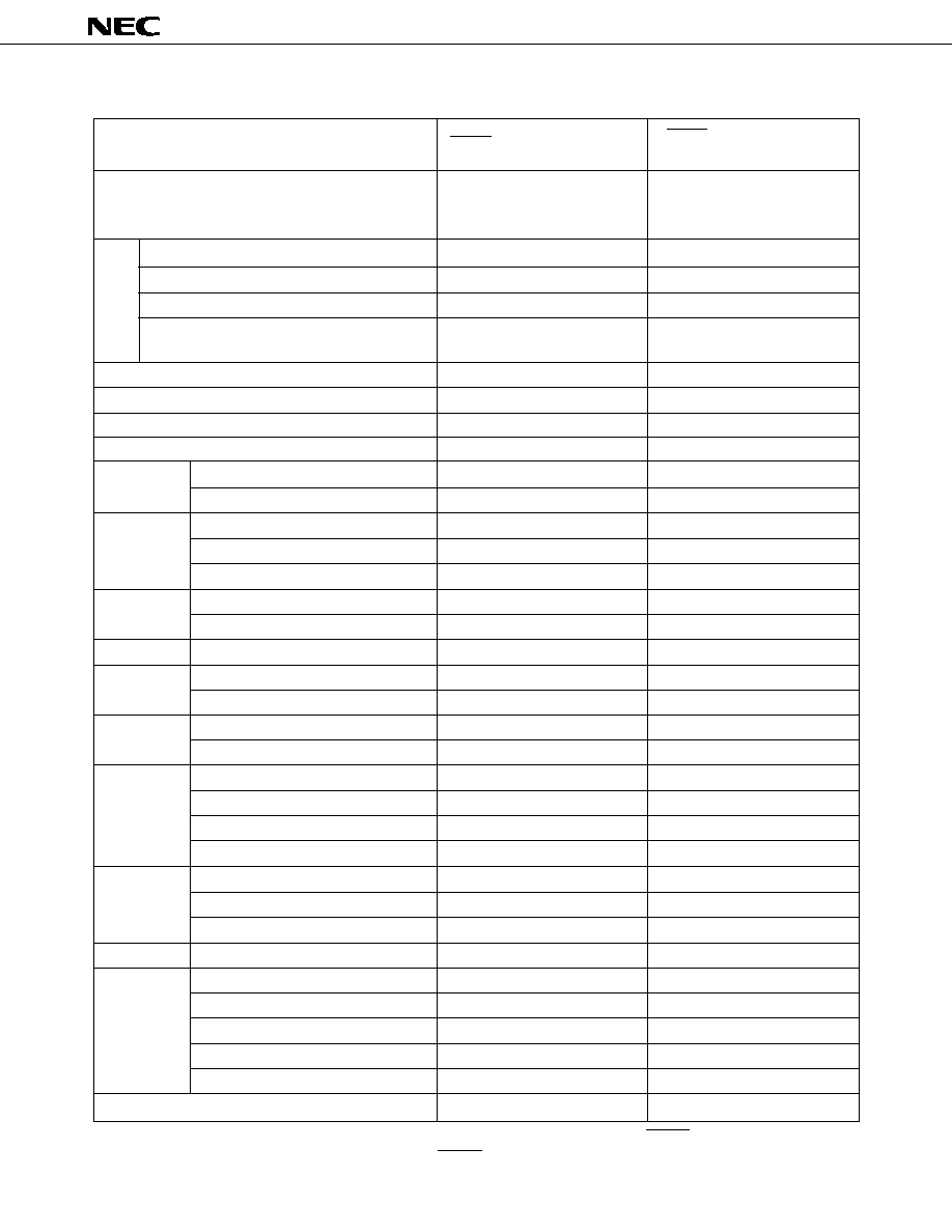
Instruction execution time
On-chip memory
ROM
RAM
General register
Input/output port
FIP dual-function pin
included
FIP dedicated pin
excluded
FIP controller/driver
Timer
Serial interface
Vectored interrupt
Test input
System clock oscillator
Standby function
Mask option
Operating temperature range
Operating voltage
Package
· 0.95, 1.91, 15.3
µ
s (Main system clock : 4.19 MHz operation)
· 122
µ
s (Subsystem clock : 32.768 kHz operation)
12160
×
8 bits
512
×
4 bits
· 4-bit manipulation : 8
×
4 banks
· 8-bit manipulation : 4
×
4 banks
33
8
CMOS input pin
20
CMOS input/output pins
· Direct LED drive capability : 8
· On-chip pull-down resistor by mask option capability : 4
1
CMOS output pin
PWM/pulse output
4
P-ch open-drain,
· LED drive capability
high-voltage,
· On-chip pull-down resistor by mask option capability
high-current output pin
· No. of segments : 9 to 16 segments
· No. of digits
: 9 to 16 digits
· Dimmer function : 8 levels
· On-chip pull-down resistor by mask option capability
· Key scan interrupt generation
4 channels
· Timer/pulse generator : 14-bit PWM output enabled
· Watch timer
: Buzzer output enabled
· Timer/event counter
· Basic interval timer
: Watchdog timer application capability
· MSB start/LSB start switchable
· Serial bus configuration capability
External : 3, Internal : 5
External : 1, Internal : 1
· Ceramic/crystal oscillator for main system clock oscillation : 4.194304 MHz standard
· Crystal oscillator for subsystem clock oscillation : 32.768 kHz standard
STOP/HALT mode
· Power-on reset, power-on flag
· High-voltage port : Pull-down resistor or open-drain output
· Port 6 : Pull-down resistor
40 to +85
°
C
2.7 to 6.0 V (standby data retention : 2.0 to 6.0 V)
· 64-pin plastic shrink DIP (750 mil)
· 64-pin plastic QFP (14
×
20 mm)
Item
Function
®
LIST OF FUNCTIONS

4
µ
PD75212A
CONTENTS
1.
PIN CONFIGURATION (TOP VIEW) ......................................................................................................... 6
2.
BLOCK DIAGRAM ...................................................................................................................................... 8
3.
PIN FUNCTIONS ........................................................................................................................................ 9
3.1 PORT PINS ............................................................................................................................................................. 9
3.2 NON-PORT PINS .................................................................................................................................................. 10
3.3 PIN INPUT/OUTPUT CIRCUIT LIST .................................................................................................................... 11
3.4 UNUSED PINS TREATMENT .............................................................................................................................. 12
3.5 P00/INT4 PIN AND RESET PIN OPERATING PRECAUTIONS ......................................................................... 13
3.6 XT1, XT2 AND P50 PIN OPERATING PRECAUTIONS ..................................................................................... 13
4.
MEMORY CONFIGURATION ................................................................................................................... 14
5.
PERIPHERAL HARDWARE FUNCTIONS ................................................................................................. 17
5.1 PORTS .................................................................................................................................................................... 17
5.2 CLOCK GENERATOR ............................................................................................................................................ 18
5.3 BASIC INTERVAL TIMER ..................................................................................................................................... 19
5.4 WATCH TIMER ...................................................................................................................................................... 20
5.5 TIMER/EVENT COUNTER ................................................................................................................................... 21
5.6 TIMER/PULSE GENERATOR ............................................................................................................................... 22
5.7 SERIAL INTERFACE ............................................................................................................................................. 23
5.8 FIP CONTROLLER /DRIVER ................................................................................................................................ 25
5.9 POWER-ON FLAG (MASK OPTION) ................................................................................................................... 27
6.
INTERRUPT FUNCTIONS ......................................................................................................................... 28
7.
STANDBY FUNCTIONS ............................................................................................................................ 30
8.
RESET FUNCTIONS .................................................................................................................................. 31
9.
INSTRUCTION SET ................................................................................................................................... 34
10. MASK OPTION SELECTION .................................................................................................................... 43
11. APPLICATION BLOCK DIAGRAM ............................................................................................................ 44
11.1 VCR TIMER TUNER ............................................................................................................................................. 44
11.2 CD PLAYER .......................................................................................................................................................... 45
11.3 ECR ....................................................................................................................................................................... 45
12. ELECTRICAL SPECIFICATIONS ............................................................................................................... 46
13. CHARACTERISTIC CURVES .................................................................................................................... 59
14. PACKAGE INFORMATION ....................................................................................................................... 63

5
µ
PD75212A
15. RECOMMENDED SOLDERING CONDITIONS ........................................................................................ 66
APPENDIX A. DEVELOPMENT TOOLS ......................................................................................................... 67
APPENDIX B. RELATED DOCUMENTS ......................................................................................................... 68
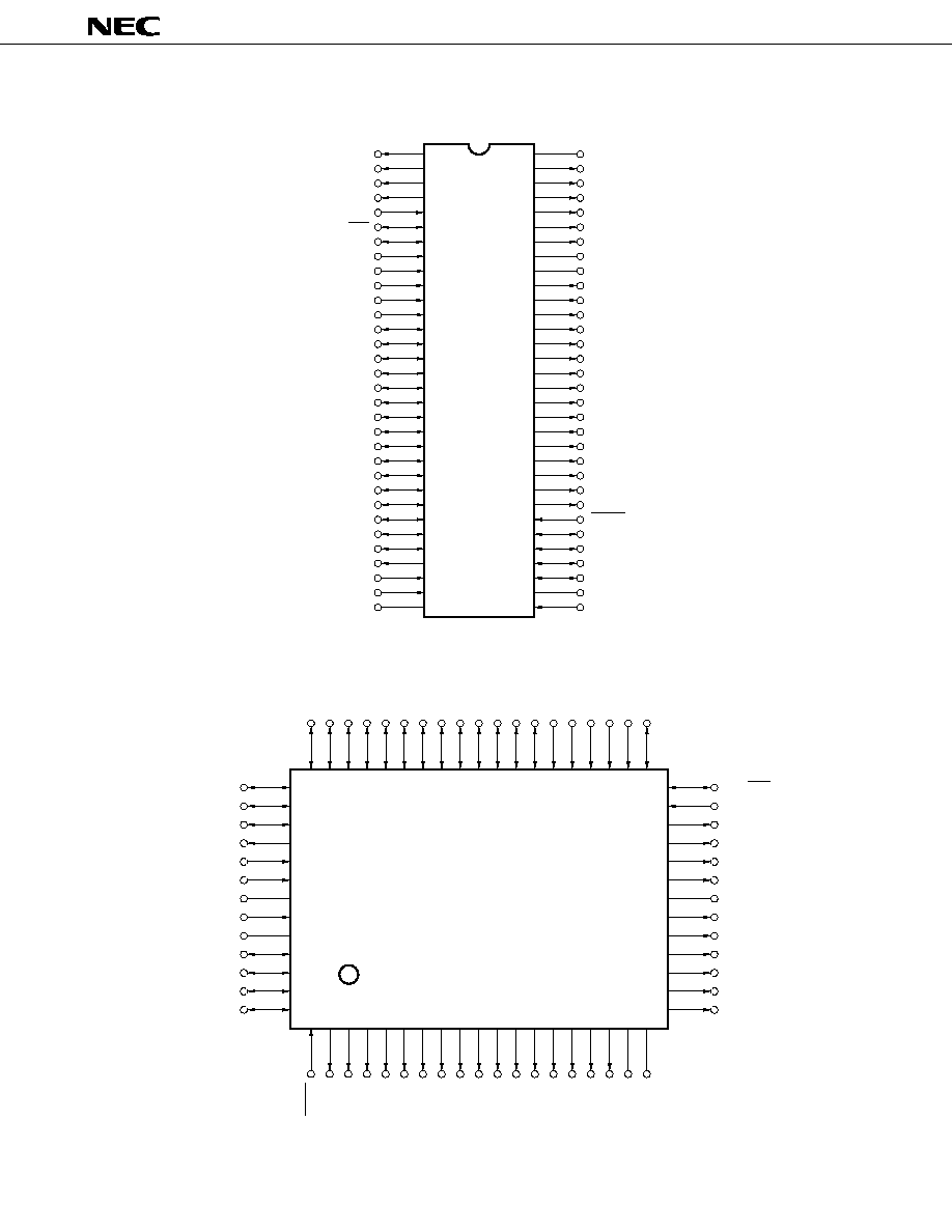
6
µ
PD75212A
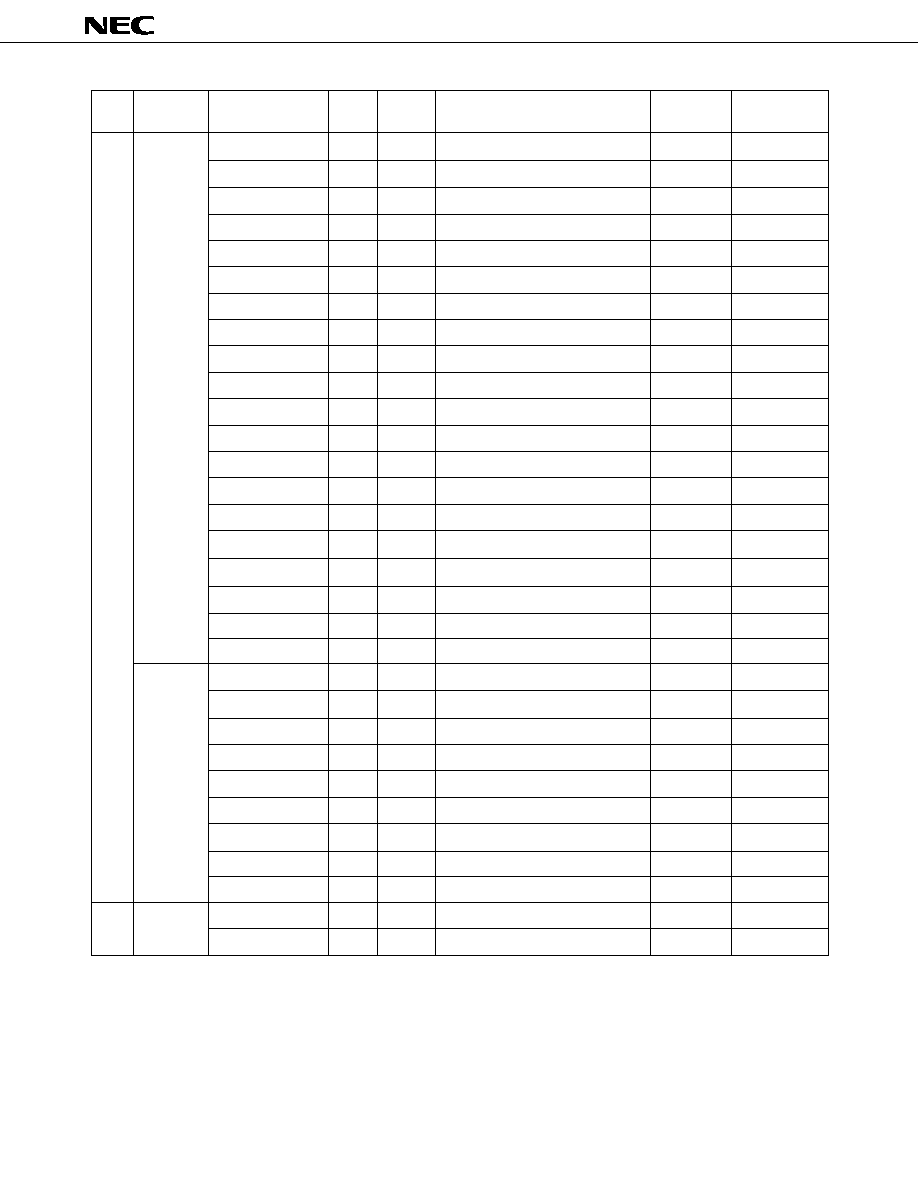
S3
S2
S1
S0
P00/INT4
P01/SCK
P02/SO
P03/SI
P10/INT0
P11/INT1
P12/INT2
P13/TI0
P20
P21
P22
P23/BUZ
P30
P31
P32
P33
P60
P61
P62
P63
P40
P41
P42
P43
PPO
X1
X2
V
SS
64
63
62
61
60
59
58
57
56
55
54
53
52
51
50
49
48
47
46
45
44
43
42
41
40
39
38
37
36
35
34
33
1
2
3
4
5
6
7
8
9
10
11
12
13
14
15
16
17
18
19
20
21
22
23
24
25
26
27
28
29
30
31
32
V
DD
S4
S5
S6
S7
S8
S9
V
PRE
V
LOAD
T15/S10
T14/S11
T13/S12/PH0
T12/S13/PH1
T11/S14/PH2
T10/S15/PH3
T9
T8
T7
T6
T5
T4
T3
T2
T1
T0
RESET
P53
P52
P51
P50
XT2
XT1
P41
P42
P43
PPO
X1
X2
V
SS
XT1
XT2
P50
P51
P52
P53
32
31
30
29
28
27
26
25
24
23
22
21
20
P01/SCK
P00/INT4
S0
S1
S2
S3
V
DD
S4
S5
S6
S7
S8
S9
51 50 49 48 47 46 45 44 43 42 41 40 39 38 37 36 35 34 33
1 2 3 4
5 6 7 8 9 10 11 12 13 14 15 16 17 18 19
52
53
54
55
56
57
58
59
60
61
62
63
64
P40
P63
P62
P61
P60
P33
P32
P31
P30
P23/BUZ
P22
P21
P20
P13/TI0
P12/INT2
P11/INT1
P10/INT0
P03/SI
P02/SO
RESET
T0
T1
T2
T3
T4
T5
T6
T7
T8
T9
V
PRE
T10/S15/PH3
T11/S14/PH2
T12/S13/PH1
T13/S12/PH0
T14/S11
T15/S10
V
LOAD
1.
PIN CONFIGURATION (TOP VIEW)
µ
PD75212ACW-
×××
µ
PD75212AGF-
×××
-3BE

7
µ
PD75212A
PIN NAME
P00-P03
: Port 0
P10-P13
: Port 1
P20-P23
: Port 2
P30-P33
: Port 3
P40-P43
: Port 4
P50-P53
: Port 5
P60-P63
: Port 6
PH0-PH3 : Port H
T0-T15
: Digit Output 0-15
S0-S15
: Segment Output 0-15
PPO
: Pulse Output
BUZ
: Fixed Frequency Output
SCK
: Serial Clock
SO
: Serial Output
SI
: Serial Input
INT0, INT1, INT4 : External Vectored Interrupt 0, 1, 4
INT2
: External Test Input 2
TI0
: Timer Input 0
X1, X2
: Main System Clock Oscillation 1, 2
XT1, XT2
: Subsystem Clock Oscillation 1, 2
RESET
: Reset Input
V
LOAD
, V
PRE
: FIP Driver Power Supply Pin
8
µ
PD75212A
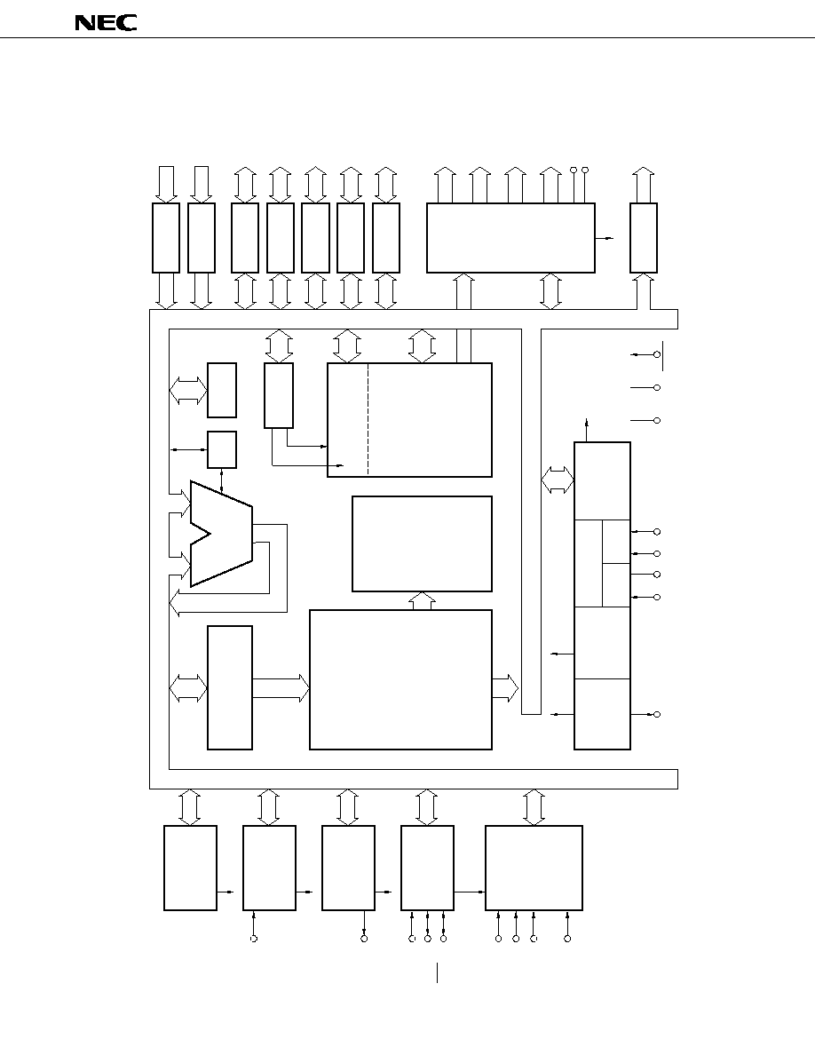
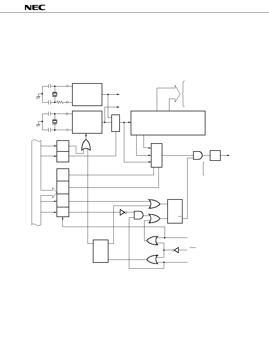
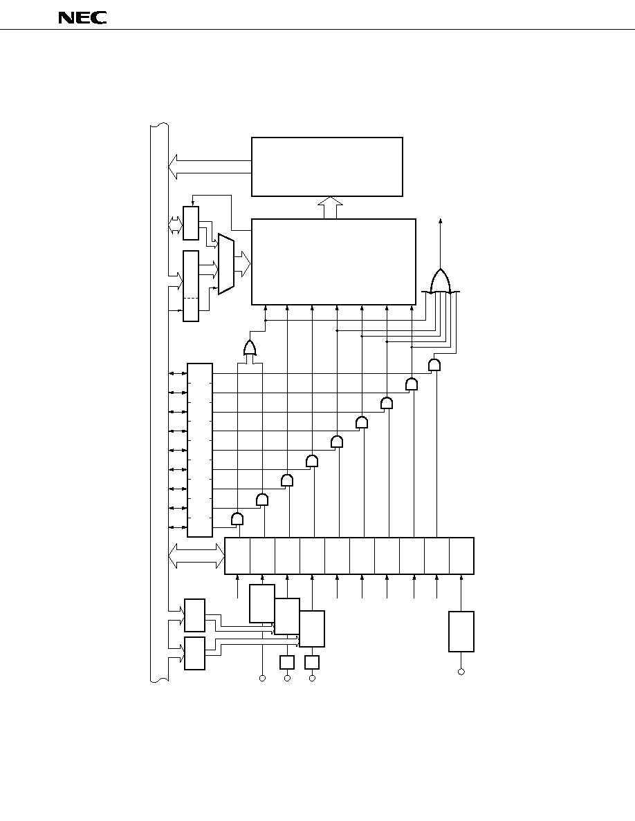
2.
BLOCK DIAGRAM
BASIC
INTERVAL
TIMER
TIMER/EVENT
COUNTER
#0
TIMER/PULSE
GENERATOR
INTBT
INTT0
INTTPG
SERIAL
INTERFACE
INTERRUPT
CONTROL
INTSIO
TI0/P13
PPO
SI/P03
SO/P02
SCK/P01
INT0/P10
INT1/P11
INT2/P12
INT4/P00
BUZ/P23
WATCH
TIMER
INTW
f
X
/2
N
CLOCK
DIVIDER
SYSTEM CLOCK
GENERATOR
SUB
MAIN
STAND BY
CONTROL
XT1 XT2 X1 X2
V
DD
V
SS
RESET
CPU CLOCK
PROGRAM
COUNTER(14)
ROM
PROGRAM
MEMORY
12160
×
8 BITS
DECODE
AND
CONTROL
RAM
DATA MEMORY
512
×
4 BITS
GENERAL REG.
BANK
SP(8)
CY
ALU
PORT0
4
P00P03
PORT1
4
P10P13
PORT2
4
P20P23
PORT3
4
P30P33
PORT4
4
P40P43
PORT5
4
P50P53
PORT6
4
P60P63
FIP
CONTROLLER/
DRIVER
10
T0T9
4
T10/S15/PH3
T13/S12/PH0
2
T14/S11,T15/
S10
10
S0S9
V
PRE
V
LOAD
PORTH
4
PH0PH3
INTKS
9
µ
PD75212A
Input
Input
Input
Input/
output
B
F
G
B
INT4
SCK
SO
SI
INT0
INT1
INT2
TI0
BUZ
T13/S12
T12/S13
T11/S14
T10/S15
P00
P01
P02
P03
P10
P11
P12
P13
P20
P21
P22
P23
P30 to P33
P40 to P43
P50 to P53
P60 to P63
PH0
PH1
PH2
PH3
3.
PIN FUNCTIONS
3.1
PORT PINS
After Reset
Function
Input/output
Input/output
4-bit input port (PORT0).
×
Input
B
Input
Noise elimination function available
Noise elimination function available
4-bit input port (PORT1).
4-bit input/output port (PORT2).
Input
E
×
Programmable 4-bit input/output port (PORT3).
Input/output specifiable in bit-wise.
Input/
output
Input
E
Input/
output
4-bit input/output port (PORT4).
LED direct drive capability.
q
q
Input
E
Input/
output
4-bit input/output port (PORT5).
LED direct drive capability.
Input
E
Input/
output
Programmable 4-bit input/output port (PORT6).
Input/output specifiable in bit-wise.
On-chip pull-down resistor available (mask
option). Suitable for key input.
×
Input
V
Output
4-bit P-ch open-drain, high-voltage, high-current
output port (PORTH).
LED direct drive capability. On-chip pull-down
resistor available (mask option).
×
I
*
Schmitt-triggered inputs are circled.
Low level
(with an on-
chip pull-
down resistor)
or high
impedance.
Dual-
Function Pin
8-Bit
I/O
Input / Output
Circuit Type *
Pin Name
I/O
10
µ
PD75212A
Segment output high-voltage output.
Static output also possible.
Pin Name
I/O
After Reset
Digit/segment output dual-function
high-voltage high-current output.
Extra pins can be used as PORTH.
Digit output high-voltage high-current
output.
FIP controller/
driver output
pins.
Pull-down
resistor can be
incorporated in
bit-wise (mask
option).
T0 to T9
Digit/segment output dual-function
high-voltage high-current output.
Static output also possible.
T10/S15 to
T13/S12
T14/S11,
T15/S10
S9
Output
PH3 to PH0
Low
level
(With an on-
chip pull-
down
resistor) or
high
impedance
(without a
pull-down
resistor)
I
3.2
NON-PORT PINS
*
Schmitt-triggered inputs are circled.
B
F
Segment high-voltage output.
S0 to S8
High
impedance
PPO
Output
Input
Timer/pulse generator pulse output.
External event pulse input for timer/event counter.
P13
Serial clock input/output.
TI0
SCK
Serial data output pin or serial data input/output.
Serial data input or normal input.
Edge-detected vectored interrupt input (rising and falling
edge detection).
INT0
INT1
SO
SI
INT4
Input/output
Input
Input
Input
P01
P02
P03
P00
P10
P11
Edge-detected vectored interrupt input with noise
elimination function (detection edge selection possible).
Edge-detected testable input (rising edge detection).
Fixed frequency output (for buzzer or system clock
trimming).
Crystal/ceramic connect pin for main system clock
oscillation.
External clock input to X1 and its inverted clock input to
X2.
Crystal connect pin for subsystem clock oscillation.
External clock input to XT1 and XT2 open.
INT2
Input
Input/output
P12
P23
BUZ
X1, X2
XT1
Input
Input
FIP controller/driver output buffer power supply.
FIP controller/driver pull-down resistor connect pin.
GND potential.
XT2
System reset input (low level active).
RESET
V
PRE
Input
Positive power supply.
V
LOAD
V
DD
V
SS
D
Input
B
Input
G
Input
B
B
B
B
Input
E
I
I
Input/output
Dual-
Function Pin
Function
Input / Output
Circuit Type *
11
µ
PD75212A
3.3
PIN INPUT/OUTPUT CIRCUIT LIST
TYPE A
TYPE B
TYPE D
TYPE E
TYPE F
TYPE G
TYPE V
TYPE I
V
DD
P-ch
N-ch
IN
IN
V
DD
P-ch
N-ch
OUT
data
output
disable
data
output
disable
Type D
IN/OUT
Type A
data
output
disable
Type D
IN/OUT
Type B
data
output
disable
Type D
IN/OUT
Type A
V
DD
P-ch
N-ch
IN/OUT
data
P-ch output
disable
Type B
V
DD
P-ch
N-ch
OUT
data
V
DD
P-ch
V
LOAD
V
PRE
CMOS-Specified Input Buffer
Schmitt-Triggered Input Having Hysteresis Characteristics
Push-Pull Output which can be Set to Output High Impedance
(with Both P-ch and N-ch Set to OFF)
Input/Output Circuit Consisting of Type D Push-Pull Output
and Type A Input Buffer
Pull-down Resistor
(Mask Option)
Pull-down
Resistor
(Mask Option)
Input/Output Circuit Capable of Switching between Push-Pull
Output and N-ch Open-Drain Output (with P-ch OFF).
Input/Output Circuit Consisting of Type D Push-Pull Output
and Type B Schmitt-Triggered Input
12
µ
PD75212A
3.4
UNUSED PINS TREATMENT
P00/INT4
P01/SCK
P02/SO
P03/SI
P10/INT0 to P12/INT2
P13/TI0
P20 to P22
P23/BUZ
P30 to P33
P40 to P43
P50 to P53
P60 to P63
PPO
S0 to S9
T15/S10 to T14/S11
T0 to T9
T10/S15/PH3 to T13/S12/PH0
XT1
XT2
RESET when there is an on-
chip power-on reset circuit
V
LOAD
when there is no on-
chip load resistor
Connect to V
SS
Connect to V
SS
or V
DD
Connect to V
SS
Input state : Connect to V
SS
or V
DD
Ouput state : Leave open
Leave open
Connect to V
SS
or V
DD
Leave open
Connect to V
DD
Connect to V
SS
or V
DD
Recommended Connection
Pin
13
µ
PD75212A
3.5
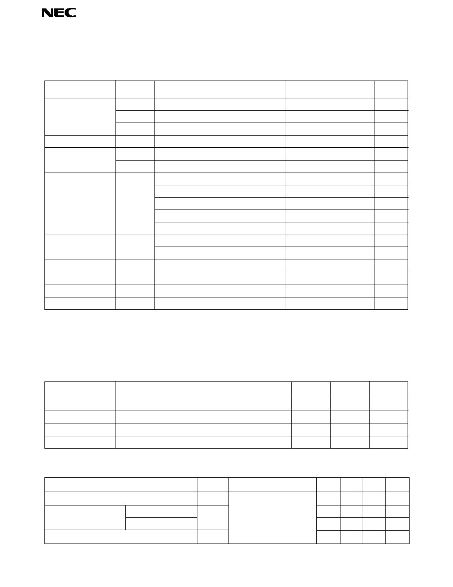
P00/INT4 PIN AND RESET PIN OPERATING PRECAUTIONS
P00/INT4 and RESET pins have the function (especially for IC test) to test
µ
PD75212A internal operations in
addition to the functions described in sections 3.1 and 3.2.
The test mode is set when a voltage larger than V
DD
is applied to one of these pins. If noise larger than V
DD
is
applied in normal operation, the test mode may be set thereby adversely affecting normal operation.
Since there is a display output pin having a high-voltage amplitude (35 V) next to the P00/INT4 and RESET pins,
if cables for the related signals are routed in parallel, wiring noise larger than V
DD
may be applied to the P00/INT4
and RESET pins causing errors.
Thus, carry out wiring so that wiring noise can be minimized, If noise still cannot be suppressed, take the measure
against noise using the following external components.
·
Connect diode with small V
F
(0.3 V or less) between
V
DD
and P00/INT4, RESET
·
Connect a capacitor between the pins and V
DD
.
V
DD
V
DD
P00/INT4, RESET
V
DD
V
DD
P00/INT4, RESET
3.6
XT1, XT2 AND P50 PIN OPERATING PRECAUTIONS
When selecting the 32.768 kHz subsystem clock connected to the XT1 and XT2 pins as the watch timer source
clock, the signal to be input or output to the P50 pin next to the XT2 pin must be a signal required to be switched
between high and low the minimum number of times (once or less per second).
If the P50 pin signal is switched frequently between high and low, a spike is generated in the XT2 pin because
of capacitance coupling of the P50 and XT2 pins and the correct watch functions cannot be achieved (the watch
becomes fast).
If it is necessary to allow the P50 pin signal to switch between high and low, mount an external capacitor to the
P50 pin as shown below.
XT1
32.768 kHz
0.0068 F
µ
XT2
P50
µ
PD75212A

14
µ
PD75212A
4.
MEMORY CONFIGURATION
·
Program memory (ROM) ................................. 12160 words
×
8 bits
· 0000H to 0001H : Vector table for writing program start address by reset
· 0002H to 000FH : Vector table for writing program start address by interrupt
· 0020H to 007FH : Table area to be referred to by GETI instruction
·
Data Memory
· Data area ....................................................... 512 words
×
4 bits (000H to 1FFH)
· Peripheral hardware area ............................ 128 words
×
4 bits (F80H to FFFH)
15
µ
PD75212A
Fig. 4-1 Program Memory Map
MBE RBE
MBE RBE
MBE RBE
MBE RBE
MBE RBE
MBE RBE
MBE RBE
MBE
6
INTBT/INT4 Start Address
Internal Reset Start Address (Most Significant 6 Bits)
Internal Reset Start Address (Least Significant 8 Bits)
(Most Significant 6 Bits)
INTBT/INT4 Start Address
(Least Significant 8 Bits)
INT0 Start Address
(Most Significant 6 Bits)
INT0 Start Address
(Least Significant 8 Bits)
INTCSIO Start Address
(Most Significant 6 Bits)
INTCSIO Start Address
(Least Significant 8 Bits)
INTT0 Start Address
(Most Significant 6 Bits)
INTT0 Start Address
(Least Significant 8 Bits)
INTTPG Start Address
(Most Significant 6 Bits)
INTTPG Start Address
(Least Significant 8 Bits)
INTKS Start Address
(Most Significant 6 Bits)
INTKS Start Address
(Least Significant 8 Bits)
(Most Significant 6 Bits)
(Least Significant 8 Bits)
INT1 Start Address
INT1 Start Address
GETI Instruction Reference Table
0 0 0 2 H
0 0 0 4 H
0 0 0 6 H
0 0 0 8 H
0 0 0 A H
0 0 0 C H
0 0 0 E H
0 0 0 0 H
0 0 2 0 H
0 0 7 F H
0 0 8 0 H
0 7 F F H
0 8 0 0 H
0 F F F H
1 0 0 0 H
1 F F F H
2 0 0 0 H
2 F 7 F H
CALLF
!faddr
Instruction
Entry Address
BRCB
!caddr
Instruction
Branch Address
BR !addr
Instruction
Branch Address
CALL !addr
Instruction
Subroutine Entry
Address
BR $ addr Instruction
Relative Branch
Address
(-15 to -1 and +2 to +16)
BRCB
!caddr Instruction
Branch Address
BRCB
!caddr Instruction
Branch Address
Branch Destination
Address and
Subroutine Entry
Address to be Set
by GETI Instruction
A d d r e s s
7
RBE
0
Remarks
In all cases other than those listed above, branch to the address with only the lower 8 bits of the PC
changed is enabled by BR PCDE and BR PCXA instructions.
16
µ
PD75212A
Fig. 4-2 Data Memory Map
(32
×
4)
256
×
4
(64
×
4)
256
×
4
128
×
4
Not Incorporated
F 8 0 H
F F F H
1 F F H
1 C 0 H
1 B F H
1 0 0 H
0 F F H
0 2 0 H
0 0 0 H
General
Register
Area
Display Data
Memory,
etc.
0 1 F H
General
Static RAM
(512
×
4)
Stack Area
Peripheral
Hardware
Area
Bank 0
Bank 1
Bank 15
17
µ
PD75212A
5.
PERIPHERAL HARDWARE FUNCTIONS
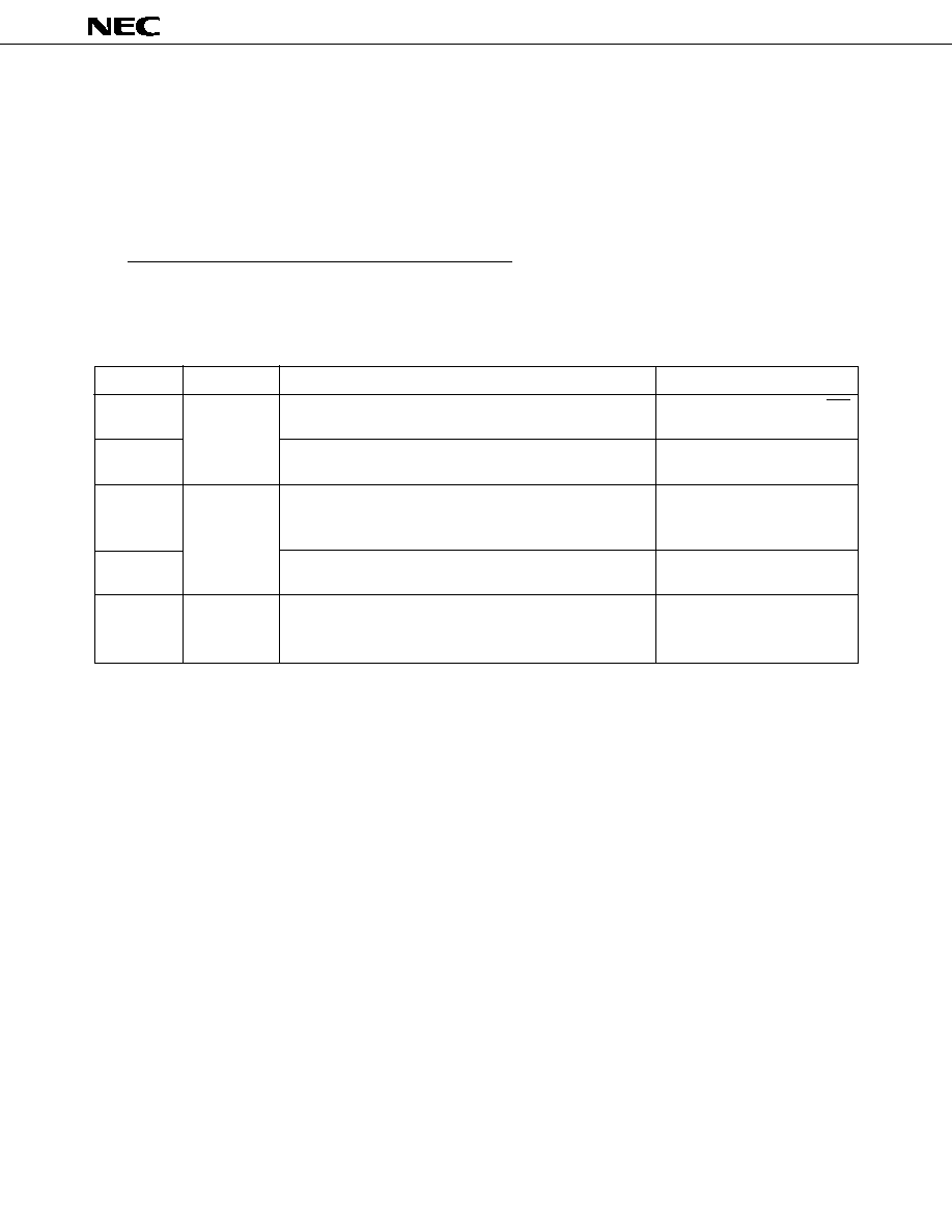
5.1
PORTS
I/O ports have the following three functions.
·
CMOS input
: 8
·
CMOS input/output
: 20
·
P-ch open-drain, high-voltage, high-current output : 4
Total
32
Table 5-1 Port Functions
Remarks
Port Name
Always read or test possible irrespective of the dual-function
pin operating mode.
Always read or test possible, P10 and P11 are inputs with the
noise elimination function.
Can be set to the input or output mode in 4-bit units.
Ports 4 and 5 can input/output data in pairs in 8-bit units.
Ports 4 and 5 can directly drive LEDs.
Can be set bit-wise to the input or output mode. Port 6 can
incorporate a pull-down resistor as a mask option.
P-ch open-drain high-voltage, high-current output port. Can
drive an FIP and LED directly. Can incorporate a pull-down
resistor bit-wise as a mask option.
Shares the pins with SI, SO, SCK
and INT4.
Shares the pins with INT0 to INT
2 and TI0.
P23 shares the pin with BUZ.
Shares the pins with T10/S15 to
T13/S12.
Operation and Feature
Function
4-bit input
PORT0
PORT1
PORT2
PORT4
PORT5
PORT3
PORT6
4-bit
input/output
PORTH
4-bit output
18
µ
PD75212A
5.2
CLOCK GENERATOR
The clock generator operations are determined by the processor clock control register (PCC) and the system clock
control register (SCC).
The clock generator has two types: main system clock and subsystem clock.
The instruction execution time can be changed.
·
0.95
µ
s, 1.91
µ
s, 15.3
µ
s (Main system clock: at 4.19 MHz operation)
·
122
µ
s (Subsystem clock: at 32.768 kHz operation)
Fig. 5-1 Clock Generator Block Diagram
XT1
XT2
X1
X2
f
XT
f
X
SCC
PCC
HALT*
STOP*
HALT F/F
STOP F/F
4
Q
S
R
S
R
1/4
1/8~1/4096
SCC3
SCC0
PCC0
PCC1
PCC2
PCC3
Q
Selector
f
XX
1/2 1/6
Frequency Divider
Selector
Watch Timer
Timer/Pulse
Generator
Subsystem
Clock
Oscillator
Main System
Clock
Oscillator
Oscillation
Stop
Frequency
Divider
· FIP Controller
· Basic Interval Timer (BT)
· Timer/Event Counter
· Serial Interface
· Watch Timer
· INT0 Noise Eliminator
· CPU
· INT0 Noise Eliminator
· INT1 Noise Eliminator
Wait Release Signal from BT
RES Signal (Internal Reset)
Standby Release Signal from
Interrupt Control Circuit
PCC2 and
PCC3
Clear
Internal Bus
*
Instruction execution
Remarks
1.
f
X
= Main system clock frequency
2.
f
XT
= Subsystem clock frequency
3.
f
XX
= System clock frequency
4.
= CPU clock
5.
PCC: Processor clock control register
6.
SCC: System clock control register
7.
1 clock cycle (t
CY
) of
is 1 machine cycle of an instruction. For t
CY
, see "AC Characteristics" in 12.
ELECTRICAL SPECIFICATIONS.
19
µ
PD75212A
*
Instruction execution
5.3
BASIC INTERVAL TIMER
The basic interval timer has the following functions:
·
Interval timer operation to generate reference time
·
Watchdog timer application to detect inadvertent program loop
·
Wait time select and count upon standby mode release
·
Count contents read
Fig. 5-2 Basic Interval Timer Configuration
Internal Bus
f
XX
/2
5
f
XX
/2
7
f
XX
/2
12
From Clock
Generator
4
BTM3
BTM2
BTM1
BTM0
BTM
MPX
BT
IRQBT
Set
BT Interrupt
Request Flag
Clear
Clear
Basic Interval Timer
(8-Bit Frequency Divider)
Wait Release
Signal During
Standby Release
8
3
Vectored
Interrupt
Request
Signal
f
XX
/2
9
SET1*
20
µ
PD75212A
5.4
WATCH TIMER
The
µ
PD75212A incorporates one channel of watch timer. The watch timer has the following functions.
·
Sets the test flag (IRQW) at 0.5-second intervals.
The standby mode can be released by IRQW.
·
0.5-second interval can be set with the main system clock and subsystem clock.
·
The fast mode enables to set 128-time (3.91 ms) interval useful to program debugging and inspection.
·
The fixed frequencies (2.048 kHz) can be output to the P23/BUZ pin for use to generate buzzer sound and trim
the system clock oscillator frequency.
·
Since the frequency divider can be cleared, the watch can be started from zero second.
Fig. 5-3 Watch Timer Block Diagram
8
Internal Bus
WM7 WM6 WM5 WM4
WM2 WM1 WM0
P23
Output
Latch
Port 2
Input/Output
Mode
PORT2.3
Bit 2 of PMGB
P23/BUZ
Output Buffer
Selector
Frequency Divider
Clear
(2.048 kHz)
2
14
f
W
2
7
f
W
(256 Hz : 3.91 ms)
f
W
(32.768 kHz)
Selector
WM
From
Clock
Generator
16
f
W
128
f
XX
(32.768 kHz)
f
XT
(32.768 kHz)
INTW
IRQW
Set Signal
2Hz
0.5 sec
WM3
Remarks
Values at f
XX
= 4.194304 MHz and f
XT
= 32.768 kHz are indicated in parentheses.
21
µ
PD75212A
5.5
TIMER/EVENT COUNTER
The
µ
PD75212A incorporates one channel of timer/event counter. The timer/event counter has the following
functions.
·
Program interval timer operation
·
Event counter operation
·
Count state read function
Fig. 5-4 Timer/Event Counter Block Diagram
P13/TI0
Input Buffer
From Clock
Generator
MPX
TMn6 TMn5 TMn4 TMn3 TMn2
SET1
TM0
Timer Operation Start
CP
Count Register (8)
Clear
8
Comparator (8)
8
8
Modulo Register (8)
8
8
Internal Bus
TMOD0
Match
IRQT0
Clear
T0
TMn7
TMn1 TMn0
*
INTT0
IRQT0
Set Signal
*
Instruction execution.
22
µ
PD75212A
5.6
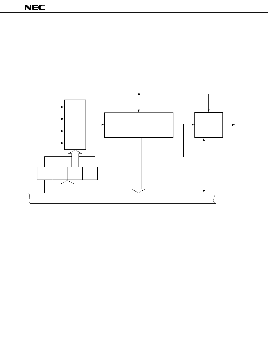
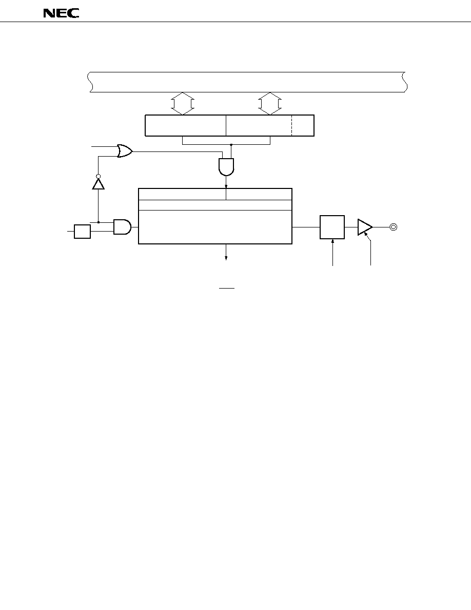
TIMER/PULSE GENERATOR
The
µ
PD75212A incorporates one channel of timer/pulse generator which can be used as a timer or a pulse
generator. The timer/pulse generator has the following functions.
(a)
Functions available in the timer mode
·
8-bit interval timer operation (IRQTPG generation) enabling the clock source to be varied at 5 levels
·
Square wave output to PPO pin
(b)
Functions available in the PWM pulse generation mode
·
14-bit accuracy PWM pulse output to the PPO pin (Used as a digital-to-analog converter and applicable
to tuning)
·
Fixed time interval ( = 7.81 ms : at 4.19 MHz operation) interrupt generation
If pulse output is not necessary, the PPO pin can be used as a 1-bit output port.
Note
If the STOP mode is set while the timer/pulse generator is in operation, miss-operation may result.
To prevent that from occurring, preset the timer/pulse generator to the stop state using its mode
register.
Fig. 5-5 Timer/Pulse Generator Block Diagram (Timer Mode)
f
XX
2
15
8
8
MODL
MODH
TPGM3
8
8
1/2
f
X
TPGM1
CP
TPGM4TPGM5 TPGM7
PPO
INTTPG
Internal Bus
Modulo Register L (8)
Modulo Register H (8)
Modulo Latch H (8)
Comparator (8)
Clear
Prescalar Select Latch (5)
Clear
Frequency
Divider
(Set to "1")
Set
T F/F
Selector
Output Buffer
IRQTPG
Set Signal
Match
Count Register (8)
23
µ
PD75212A
Fig. 5-6 Timer/Pulse Generator Block Diagram (PWM Pulse Generation Mode)
f
x
TPGM1
TPGM3
8
8
MODH
MODL
MODH (8)
PPO
TPGM5
TPGM7
INTTPG
1/2
MODL
7-2
(6)
Internal Bus
Modulo Register H (8)
Modulo Register L (6)
Frequency Divider
Modulo Latch (14)
PWM Pulse Generator
Selector
Output Buffer
(IRQTPG Set Signal)
(2)
(
= 7.81 ms : at 4.19 MHz operation)
2
15
f
X
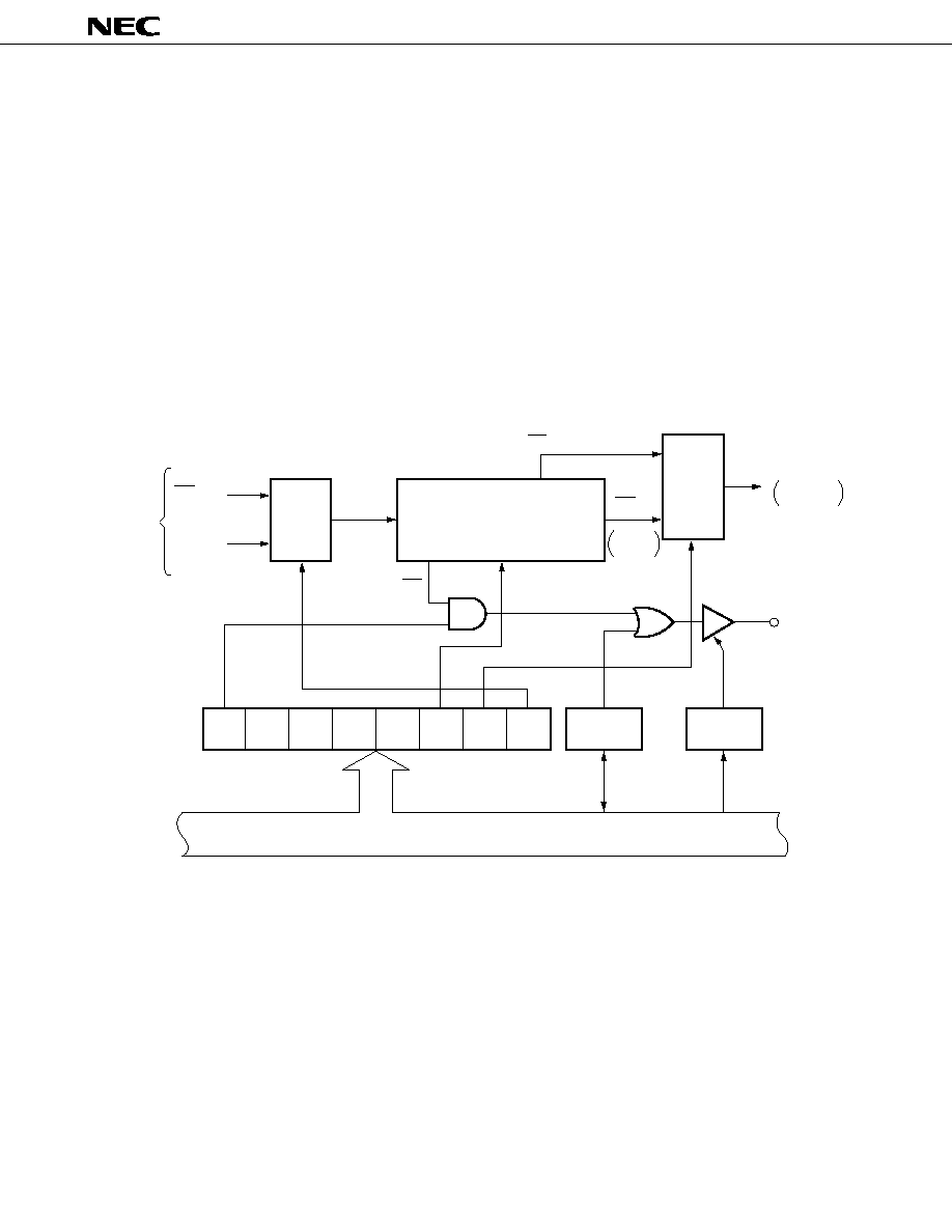
5.7
SERIAL INTERFACE
The
µ
PD75212A serial interface has the following functions.
·
Clocked 8-bit send/receive operation (simultaneous send/receive)
·
Clocked 8-bit serial bus operation (data input/output from the SO pin. N-ch open-drain SO output)
·
Start LSB/MSB switching
The above functions facilitate data communication with another microcomputer of
µ
PD7500 series and 78K series
via serial bus and coupling with peripheral devices.
24
µ
PD75212A
Fig 5-7 Serial Interface Block Diagram
*
1. CMOS output and N-ch open drain output switchable output buffer.
2. Instruction execution
Shift Register (8)
Serial Clock
Counter (3)
Clear
Overflow
Serial Start
SIOM7SIOM6SIOM5SIOM4SIOM3SIOM2SIOM1SIOM0
SIOM
SET1 *2
8
8
8
P03/SI
P02/SO
P01/SCK
SIO7
SIO
SIO0
IRQSIO
Clear Signal
f
xx
/2
10
f
xx
/2
4
MPX
R
S
Q
Internal Bus
INTSIO
IRQSIO
Set Signal
SO Output
Latch
*1
Selector
25
µ
PD75212A
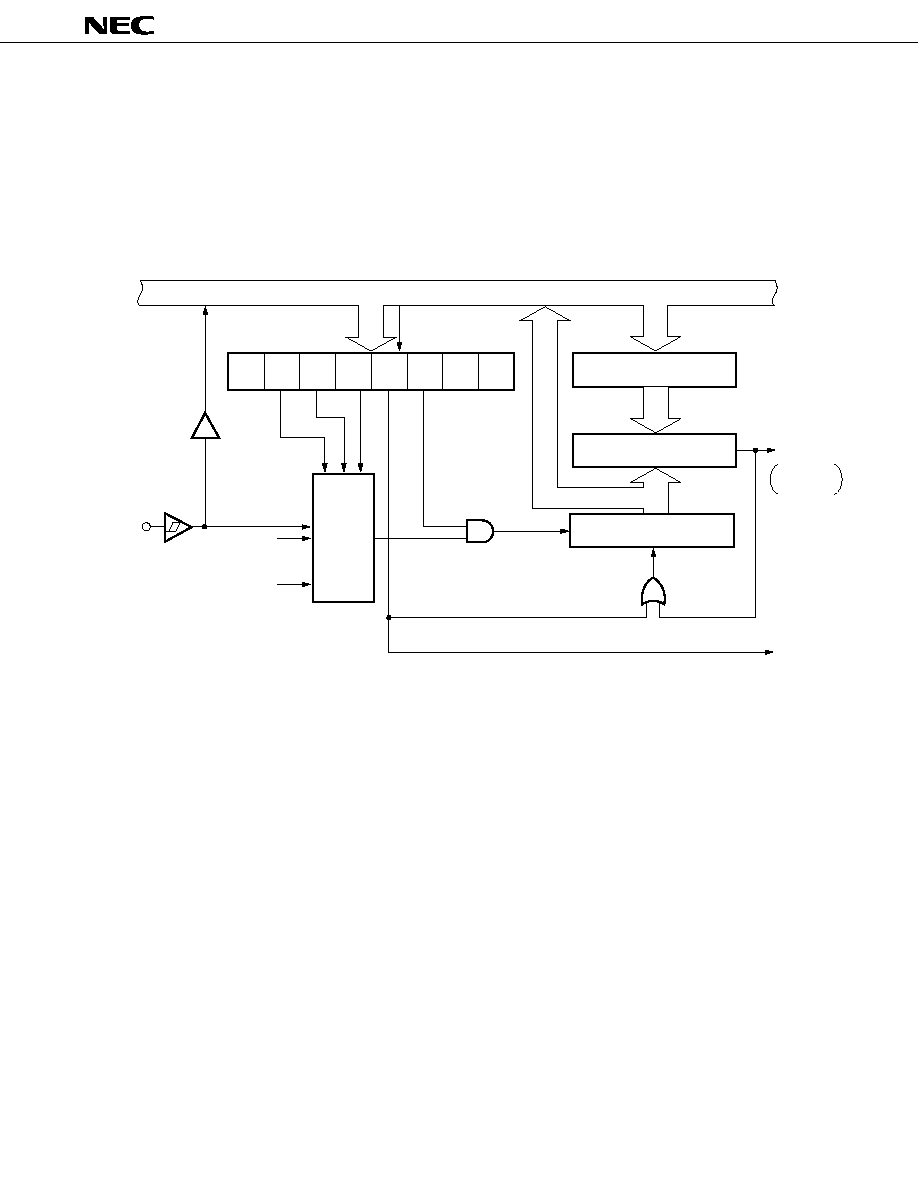
5.8
FIP CONTROLLER/DRIVER
The FIP controller/driver incorporated in the
µ
PD75212A has the following functions:
·
Generates the segment and digit signals by automatically reading the display data memory executing DMA
operation.
·
Can select up to a total of 26 display devices in the range of 9 to 16 segments and 9 to 16 digits.
·
Can apply the remaining display output as static output.
·
Can adjust the brightness at 8 levels using the dimmer function.
·
Can apply key scan operations.
· Generates interrupt at the key scan timing (IRQKS)
· Can generate key scan data output from the segment output pin.
·
Owns the high-voltage output pin (40 V) which can directly drive the FIP.
·
Segment special pins (S0 to S9)
: V
OD
= 40 V, I
OD
= 3 mA
· Digit output pins (T0 to T15)
: V
OD
= 40 V, I
OD
= 15 mA
·
Can incorporate pull-down resistors bit-wise as mask options.
Differences between
µ
PD75212A and
µ
PD75238 display output function are shown in Table 5-2.
Table 5-2 Differences between
µ
PD75212A and
µ
PD75238 Display Output Function
FIP output total
: 34
Segment output
: 9 to 24
Digit output
: 9 to 16
1A0H to 1FFH
S0 to S23
(PORT10 to PORT15)
KS0 to KS2
µ
PD75212A
FIP output total
: 26
Segment output
: 9 to 16
Digit output
: 9 to 16
1C0H to 1FFH
S12 to S15
(PORTH)
KS0, KS1
High-voltage output display
Display data area
Output dual-function pin
Key scan register
µ
PD75238
26
µ
PD75212A
4
4
4
10
12
4
4
4
4
4
4
2
10
2
2
4
2
10
10
INTKS
V
LOAD
T0-T9
T13/S12/PH0-
T10/S15/PH3
T15/S10,
T14/S11
S0-S9
Internal Bus
Selector
Selector
Segment Data Latch (16)
Display Data Memory
(64
×
4 Bits)
Key Scan Registers (KS0, KS1)
Port H
Digit Signal
Generator
IRQKS
Generation
Signal
Key Scan
Flag (KSF)
Display
Mode
Register
Digit
Select
Register
Dimmer
Select
Register
High-Voltage Output Buffer
V
PRE
Fig. 5-8 FIP Controller/Driver Block Diagram
Note
The FIP controller/driver can only operate in the high and intermediate-speeds (PCC = 0011B or
0010B) of the main system clock (SCC.0 = 0). It may cause errors with any other clock or in the
standby mode. Thus, be sure to stop FIP controller operation (DSPM.3 = 0) and then shift the unit
to any other clock mode or the standby mode.

27
µ
PD75212A
5.9
POWER-ON FLAG (MASK OPTION)
The power-on flag (PONF) is automatically set (1) when the power-on reset circuit is activated and the power-
on reset signal is generated (See Fig. 8-1 Reset Signal Generator).
The PONF is mapped at bit 0 of address FD1H in the data memory space and can be tested by the memory bit
manipulation instructions (SKT, SKF, SKTCLR) or cleared (CLR1).
Note
The PONF cannot be set by SET1 instruction.

28
µ
PD75212A
6.
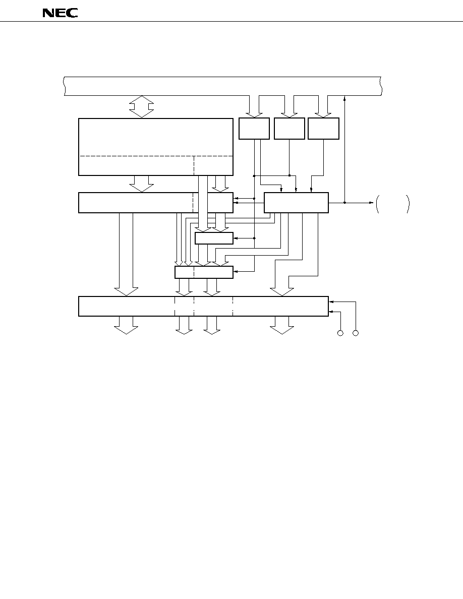
INTERRUPT FUNCTIONS
The
µ
PD75212A has eight types of interrupt sources and can generate multiple interrupts with priority order.
It is also equipped with two types of test sources. INT2 is an edge detected testable input.
The
µ
PD75212A interrupt control circuit has the following functions:
·
Hardware-controller vectored interrupt function which can control interrupt acknowledge with the interrupt
enable flag (IE
×××
) and the interrupt master enable flag (IME).
·
Function of setting any interrupt start address.
·
Multiple interrupt function which can specify priority order with the interrupt priority select register (IPS).
·
Interrupt request flag (IRQ
×××
) test function. (Interrupt generation can be checked by software.)
·
Standby mode release function. (Interrupt to be released by interrupt enable flag can be selected.)
29
µ
PD75212A
Fig. 6-1 Interrupt Control Circuit Block Diagram
*
Noise eliminator
4
2
(IME)
IPS
IST
Decoder
2
2
IM1
IM0
IRQBT
INT4
/P00
INT0
/P10
INT1
/P11
IRQ4
IRQ0
IRQ1
IRQSIO
IRQT0
IRQTPG
INT
BT
INTSIO
INTT0
INTTPG
VRQn
Internal Bus
Vector
Table
Address
Generator
Circuit
Priority Control
Circuit
Standby Release
Signal
Interrupt Enable Flag (IE
XXX
)
Edge
Detection
Circuit
Edge
Detection
Circuit
Both Edges
Detection
Circuit
INT2
/P12
Rising Edge
Detection
Circuit
INTKS
IRQW
*
*
IRQKS
IRQ2
INTW
30
µ
PD75212A
7.
STANDBY FUNCTIONS
Two standby modes (STOP mode and HALT mode) are available for the
µ
PD75212A to decrease power
consumption in the program standby mode.
Table 7-1 Operation Status in Standby Mode
HALT Mode
HALT instruction
Setting enabled with either main system
clock or subsystem clock.
Stops only with CPU clock
(Oscillation
continued).
Operation (IRQBT set at reference time
intervals).
Operation enabled when serial clock other
than
is specified.
Operation enabled.
Operation enabled.
Operation enabled.
Set instruction
System clock when set
Clock oscillator
Basic interval timer
Serial interface
Timer/event counter
Timer/pulse generator
Watch timer
FIP controller/driver
CPU
STOP Mode
STOP instruction
Setting enabled only with main system
clock.
Oscillation stops only with main system
clock.
Operation stopped.
Operation enabled only when external
SCK input is selected for serial clock.
Operation enabled only when TI0 pin
input is specified for count clock.
Operation stopped.
Operation enabled only f
XT
is selected for
count clock.
Operating State
Operation disabled (display off mode set before disabling).
Operation stopped.
Release signal
Interrupt request signal (except INT0, INT1, INT2) enabled by interrupt enable flag
or RESET input.
31
µ
PD75212A
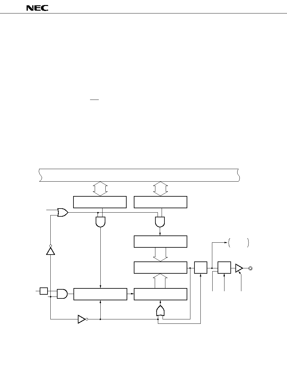
8.
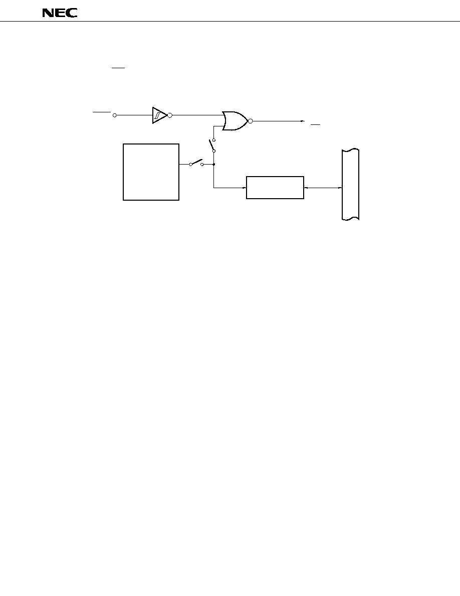
RESET FUNCTIONS
The reset signal (RES) generator has a configuration shown in Fig. 8-1.
Fig. 8-1 Reset Signal Generator
The power-on reset generator is a circuit to generate a one-shot pulse upon detection of the start-up of the power
voltage. This pulse is used in the following three ways according to SWA, SWB mask option specification shown
in Fig. 8-1. (Refer to 10. MASK OPTION SELECTION.)
RESET
Power-On
Reset
Generator
Mask
Option
Internal Reset Signal
(RES)
Power-On Flag
(PONF)
Internal Bus
Bit
Manipulation
Instruction
Execution
SWA
SWB
32
µ
PD75212A
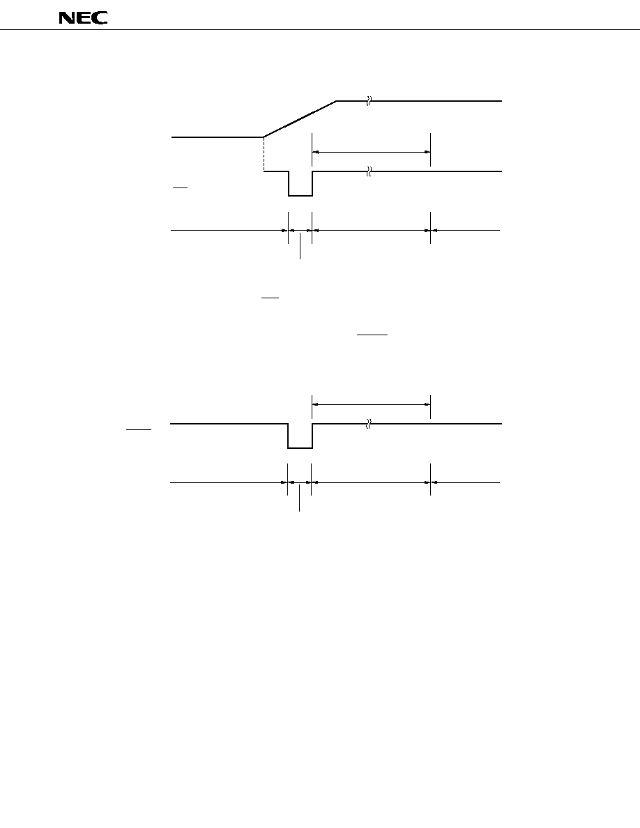
Fig. 8-2 Reset Operation by Power-On Reset
*
Wait time does not include a time from RES signal generation to oscillation start.
Fig. 8-3 Reset Operation by RESET Input
(31.3ms:4.19MHz)
Wait
RESET Input
Operating Mode or
Standby Mode
HALT Mode
Operating
Mode
Internal Reset Operation
Each hardware state after reset operation is shown in Table 8-1.
5
(31.3ms:4.19MHz)
Wait
0 V
HALT Mode
Operating
Mode
Internal Reset Operation
*
Internal Reset Signal
(RES)
Supply Voltage
5
33
µ
PD75212A
Counter (BT)
Mode register (BTM)
Counter (T0)
Modulo register (TMOD0)
Mode register (TM0)
Modulo register (MODH, MODL)
Mode register (TPGM)
Mode register (WM)
Shift register (SIO)
Mode register (SIOM)
Processor clock control register (PCC)
System clock control register (SCC)
Interrupt request flag (IRQ
×××
)
Interrupt enable flag (IE
×××
)
Priority select register (IPS)
INT0 and INT1 mode registers (IM0, IM1)
Output buffer
Output latch
Input/output mode register (PMGA, PMGB)
Output latch
Display mode register (DSPM)
Digit select register (DIGS)
Dimmer select register (DIMS)
Display data memory
Output buffer
Program counter (PC)
Carry flag (CY)
Skip flag (SK0 to SK2)
Interrupt status flag (IST0, IST1)
Bank enable flags (MBE, RBE)
Stack pointer (SP)
Data memory (RAM)
General registers (X, A, H, L, D, E, B, C)
Bank select registers (MBS, RBS)
PSW
Basic interval
timer
Timer/event
counter
Timer/pulse
generator
Watch timer
Serial
interface
Clock
generator
Interrupt
Digital port
Port H
FIP controller/
driver
Power on flag (PONF)
*
1. Data of data memory addresses 0F8H to 0FDH becomes indeterminate by RESET input.
2. 1 upon power-on reset, indeterminate after RESET input in operation.
5
Hardware
Table 8-1 Hardware Statuses after Reset
RESET Input in Standby Mode
RESET Input upon Power-on
Reset or in Operation
Sets the low-order 6 bits of program
memory address 0000H to PC
13-8
and
the contents of address 0001H to PC
7-0
.
Hold
0
0
Sets bit 6 of program memory address
0000H to RBE and bit 7 to MBE.
Undefined
Hold*1
Hold
0, 0
Undefined
0
0
FFH
0
Hold
0
0
Hold
Only bit 4 set to 1, other bits set to 0
0
0
Reset (0)
0
0
0, 0
Off
Clear (0)
0
Hold
0
1000B
0
Hold
Off
Hold
Sets the low-order 6 bits of program
memory address 0000H to PC
13-8
and
the contents of address 0001H to PC
7-0
.
Undefined
0
0
Sets bit 6 of program memory address
0000H to RBE and bit 7 to MBE.
Undefined
Undefined
Undefined
0, 0
Undefined
0
0
FFH
0
Undefined
0
0
Undefined
Only bit 4 set to 1, other bits set to 0
0
0
Reset (0)
0
0
0, 0
Off
Clear (0)
0
Undefined
0
1000B
0
Undefined
Off
1 or undefined*2
34
µ
PD75212A
9.
INSTRUCTION SET
(1)
Operand identifier and description
Enter an operand in the operand column of each instruction using the description method relating to the
operand identifier of the instruction (For details, refer to RA75X Assembler Package User's Manual Language
Volume (EEU-730)). If more than one description method is available, select one. Capital alphabetic letters, plus
and minus signs are keywords. Describe them as they are.
In the case of immediate data, describe appropriate numerical values or labels.
Symbols can be described as labels in place of mem, fmem, pmem, bit, etc. (For details, refer to
µ
PD75216A
User's Manual (IEM-988)). Available labels are limited for fmem and pmem.
Identifier
Description Method
reg
X, A, B, C, D, E, H, L
reg 1
X, B, C, D, E, H, L
rp
XA, BC, DE, HL
rp1
BC, DE, HL
rp2
BC, DE
rp'
XA, BC, DE, HL, XA', BC', DE', HL'
rp'1
BC, DE, HL, XA', BC', DE', HL'
rpa
HL, HL+, HL-, DE, DL
rpa1
DE, DL
n4
4-bit immediate data or label
n8
8-bit immediate data or label
mem
8-bit immediate data or label*
bit
2-bit immediate data or label
fmem
FB0H to FBFH and FF0H to FFFH immediate data or labels
pmem
FC0H to FFFH immediate data or labels
addr
0000H to 2F7FH immediate data or labels
caddr
12-bit immediate data or label
faddr
11-bit immediate data or label
taddr
20H to 7FH immediate data (bit0 = 0) or label
PORTn
PORT0 to PORT6
IE
×××
IEBT, IESIO, IET0, IETPG, IE0, IE1, IEKS, IEW, IE4
RBn
RB0 to RB3
MBn
MB0, MB1, MB15
*
For 8-bit data processing, only even addresses can be specified.

35
µ
PD75212A
(2)
Legend for operation description
A
: A register; 4-bit accumulator
B
: B register
C
: C register
D
: D register
E
: E register
H
: H register
L
: L register
X
: X register
XA
: Register pair (XA); 8-bit accumulator
BC
: Register pair (BC)
DE
: Register pair (DE)
HL
: Register pair (HL)
XA'
: Expanded register pair (XA')
BC'
: Expanded register pair (BC')
DE'
: Expanded register pair (DE')
HL'
: Expanded register pair (HL')
PC
: Program counter
SP
: Stack pointer
CY
: Carry flag; Bit accumulator
PSW
: Program status word
MBE
: Memory bank enable flag
RBE
: Register bank enable flag
PORTn
: Port n (n = 0 to 6)
IME
: Interrupt master enable flag
IPS
: Interrupt priority select register
IE
×××
: Interrupt enable flag
RBS
: Register bank select register
MBS
: Memory bank select register
PCC
: Processor clock control register
·
: Address and bit delimiter
(
××
)
: Contents addressed by
××
××
H
: Hexadecimal data
36
µ
PD75212A
(3)
Description of symbols in the addressing area column
Data Memory
Addressing
Program Memory
Addressing
* 1
MB = MBE · MBS
(MBS = 0, 1, 15)
* 2
MB = 0
* 3
MBE = 0 : MB = 0 (00H to 7FH)
MB = 15 (80H to FFH)
MBE = 1 : MB = MBS (MBS = 0, 1, 15)
* 4
MB = 15, fmem = FB0H to FBFH,
FF0H to FFFH
* 5
MB = 15, pmem = FC0H to FFFH
* 6
addr = 0000H to 2F7FH
* 7
addr = (Current PC) 15 to (Current PC) 1,
(Current PC) + 2 to (Current PC) + 16
* 8
caddr = 0000H to 0FFFH
(PC
13, 12
= 00B) or
1000H to 1FFFH
(PC
13, 12
= 01B) or
2000H to 2F7FH
(PC
13, 12
= 10B)
* 9
faddr = 0000H to 07FFH
*10
taddr = 0020H to 007FH
Remarks
1.
MB indicates accessible memory bank.
2.
In *2, MB = 0 irrespective of MBE and MBS.
3.
In *4 and *5, MB = 15 irrespective of MBE and MBS.
4.
*6 to *10 indicate addressable areas.
(4)
Description of the machine cycle column
S indicates the number of machine cycles required for skip operation by an instruction having skip function.
The S value varies as follows:
· When not skipped ................................................................................................... S = 0
· When 1-byte or 2-byte instructions are skipped ................................................. S = 1
· When 3-byte instructions are skipped (BR !addr, CALL !addr instruction) ..... S = 2
Note
GETI instruction is skipped in one machine cycle.
One machine cycle is equal to one cycle(=t
CY
) of CPU clock
and three time periods are available
according to PCC setting.
37
µ
PD75212A
A, #n4
1
1
A
n4
Stack A
reg1, #n4
2
2
reg1
n4
XA, #n8
2
2
XA
n8
Stack A
HL, #n8
2
2
HL
n8
Stack B
rp2, #n8
2
2
rp2
n8
A, @HL
1
1
A
(HL)
*1
A, @HL+
1
2 + S
A
(HL), then L
L+1
*1
L = 0
A, @HL
1
2 + S
A
(HL), then L
L1
*1
L = FH
A, @rpa1
1
1
A
(rpa1)
*2
XA, @HL
2
2
XA
(HL)
*1
@HL, A
1
1
(HL)
A
*1
@HL, XA
2
2
(HL)
XA
*1
A, mem
2
2
A
(mem)
*3
XA, mem
2
2
XA
(mem)
*3
mem, A
2
2
(mem)
A
*3
mem, XA
2
2
(mem)
XA
*3
A, reg
2
2
A
reg
XA, rp'
2
2
XA
rp'
reg1, A
2
2
reg1
A
rp'1, XA
2
2
rp'1
XA
A, @HL
1
1
A
(HL)
*1
A, @HL+
1
2 + S
A
(HL), then L
L+1
*1
L = 0
A, @HL
1
2 + S
A
(HL), then L
L1
*1
L = FH
A, @rpa1
1
1
A
(rpa1)
*2
XA, @HL
2
2
XA
(HL)
*1
A, mem
2
2
A
(mem)
*3
XA, mem
2
2
XA
(mem)
*3
A, reg1
1
1
A
reg1
XA, rp'
2
2
XA
rp'
XA, @PCDE
1
3
XA
(PC
138
+DE)
ROM
XA, @PCXA
1
3
XA
(PC
138
+XA)
ROM
Machine
Cycle
Skip
Condition
Addressing
Area
No. of
Bytes
Transfer
Note
1. Instruction Group
2. Table reference
Mnemonic
Operands
Operation
Note 1
MOV
XCH
MOVT
Note 2
38
µ
PD75212A
Machine
Cycle
Skip
Condition
Addressing
Area
No. of
Bytes
CY, fmem.bit
2
2
CY
(fmem.bit)
*4
CY, pmem.@L
2
2
CY
(pmem
72
+L
32
.bit(L
10
))
*5
CY, @H+mem.bit
2
2
CY
(H+mem
30
.bit)
*1
fmem.bit, CY
2
2
(fmem.bit)
CY
*4
pmem.@L, CY
2
2
(pmem
72
+L
32
.bit(L
10
))
CY
*5
@H+mem.bit, CY
2
2
(H+mem
30
.bit)
CY
*1
A, #n4
1
1 + S
A
A+n4
carry
XA, #n8
2
2 + S
XA
XA+n8
carry
A, @HL
1
1 + S
A
A+(HL)
*1
carry
XA, rp'
2
2 + S
XA
XA+rp'
carry
rp'1, XA
2
2 + S
rp'1
rp'1+XA
carry
A, @HL
1
1
A, CY
A+(HL)+CY
*1
XA, rp'
2
2
XA, CY
XA+rp'+CY
rp'1, XA
2
2
rp'1, CY
rp'1+XA+CY
A, @HL
1
1 + S
A
A(HL)
*1
borrow
XA, rp'
2
2 + S
XA
XArp'
borrow
rp'1, XA
2
2 + S
rp'1
rp'1XA
borrow
A, @HL
1
1
A, CY
A(HL)CY
*1
XA, rp'
2
2
XA, CY
XArp'CY
rp'1, XA
2
2
rp'1, CY
rp'1XACY
A, #n4
2
2
A
A n4
A, @HL
1
1
A
A (HL)
*1
XA, rp'
2
2
XA
XA rp'
rp'1, XA
2
2
rp'1
rp'1 XA
A, #n4
2
2
A
A
n4
A, @HL
1
1
A
A
(HL)
*1
XA, rp'
2
2
XA
XA
rp'
rp'1, XA
2
2
rp'1
rp'1
XA
A, #n4
2
2
A
A
n4
A, @HL
1
1
A
A
(HL)
*1
XA, rp'
2
2
XA
XA
rp'
rp'1, XA
2
2
rp'1
rp'1
XA
Bit transfer
Operation
Note
Instruction Group
Mnemonic
Operand
Operation
Note
MOV1
ADDS
ADDC
SUBS
SUBC
AND
OR
XOR
39
µ
PD75212A
A
1
1
CY
A
0
, A
3
CY, A
n1
A
n
A
2
2
A
A
reg
1
1 + S
reg
reg+1
reg = 0
rp1
1
1 + S
rp1
rp1+1
rp1 = 00H
@HL
2
2 + S
(HL)
(HL)+1
*1
(HL) = 0
mem
2
2 + S
(mem)
(mem)+1
*3
(mem) = 0
reg
1
1 + S
reg
reg1
reg = FH
rp'
2
2 + S
rp'
rp'1
rp = FFH
reg, #n4
2
2 + S
Skip if reg = n4
reg = n4
@HL, #n4
2
2 + S
Skip if (HL) = n4
*1
(HL) = n4
A, @HL
1
1 + S
Skip if A = (HL)
*1
A = (HL)
XA, @HL
2
2 + S
Skip if XA = (HL)
*1
XA = (HL)
A, reg
2
2 + S
Skip if A = reg
A = reg
XA, rp'
2
2 + S
Skip if XA = rp'
XA = rp'
CY
1
1
CY
1
CY
1
1
CY
0
CY
1
1 + S
Skip if CY = 1
CY = 1
CY
1
1
CY
CY
Machine
Cycle
Skip
Condition
Addressing
Area
No. of
Bytes
RORC
NOT
Note 2
Increment/decrement
Compare
SET1
CLR1
SKT
NOT1
Carry flag
manipulation
Note
1. Instruction Group
2. Accumulator manipulation
Operands
Mnemonic
Operation
Note 1
INCS
DECS
SKE
40
µ
PD75212A
mem.bit
2
2
(mem.bit)
1
*3
fmem.bit
2
2
(fmem.bit)
1
*4
pmem.@L
2
2
(pmem
72
+L
32
.bit(L
10
))
1
*5
@H + mem.bit
2
2
(H+mem
30
.bit)
1
*1
mem.bit
2
2
(mem.bit)
0
*3
fmem.bit
2
2
(fmem.bit)
0
*4
pmem.@L
2
2
(pmem
72
+L
32
.bit(L
10
))
0
*5
@H+mem.bit
2
2
(H+mem
30
.bit)
0
*1
mem.bit
2
2 + S
Skip if (mem.bit) = 1
*3
(mem.bit) = 1
fmem.bit
2
2 + S
Skip if (fmem.bit) = 1
*4
(fmem.bit) = 1
pmem.@L
2
2 + S
Skip if (pmem
72
+L
32
.bit(L
10
)) = 1
*5
(pmem.@L) = 1
@H+mem.bit
2
2 + S
Skip if (H+mem
30
.bit) = 1
*1
(@H+mem.bit) = 1
mem.bit
2
2 + S
Skip if (mem.bit) = 0
*3
(mem.bit) = 0
fmem.bit
2
2 + S
Skip if (fmem.bit) = 0
*4
(fmem.bit) = 0
pmem.@L
2
2 + S
Skip if (pmem
72
+L
32
.bit(L
10
)) = 0
*5
(pmem.@L) = 0
@H+mem.bit
2
2 + S
Skip if (H+mem
30
.bit) = 0
*1
(@H+mem.bit) = 0
fmem.bit
2
2 + S
Skip if (fmem.bit) = 1 and clear
*4
(fmem.bit) = 1
pmem.@L
2
2 + S
Skip if (pmem
72
+L
32
.bit(L
10
))=1 and clear
*5
(pmem.@L) = 1
@H+mem.bit
2
2 + S
Skip if (H+mem
30
.bit)=1 and clear
*1
(@H+mem.bit)=1
CY, fmem.bit
2
2
CY
CY (fmem.bit)
*4
CY, pmem.@L
2
2
CY
CY (pmem
72
+L
32
.bit(L
10
))
*5
CY, @H+mem.bit
2
2
CY
CY (H+mem
30
.bit)
*1
CY, fmem.bit
2
2
CY
CY
(fmem.bit)
*4
CY, pmem.@L
2
2
CY
CY
(pmem
72
+L
32
.bit(L
10
))
*5
CY, @H+mem.bit
2
2
CY
CY
(H+mem
30
.bit)
*1
CY, fmem.bit
2
2
CY
CY
(fmem.bit)
*4
CY, pmem.@L
2
2
CY
CY
(pmem
72
+L
32
.bit(L
10
))
*5
CY, @H+mem.bit
2
2
CY
CY
(H+mem
30
.bit)
*1
addr
--
--
PC
130
addr
*6
(Optimum instruction is
selected from among BR !addr,
BRCB !caddr and BR $addr by an
assembler.)
!addr
3
3
PC
130
addr
*6
$addr
1
2
PC
130
addr
*7
!caddr
2
2
PC
130
PC
13,12
+caddr
110
*8
PCDE
2
3
PC
130
PC
138
+DE
PCXA
2
3
PC
130
PC
138
+XA
Machine
Cycle
Skip
Condition
Addressing
Area
No. of
Bytes
Memory bit manipulation
BRCB
Branch
Note
Instruction Group
Mnemonic
Operands
Operation
Note
SET1
CLR1
SKT
SKF
SKTCLR
AND1
OR1
XOR1
BR
BR
41
µ
PD75212A
!addr
3
3
(SP4) (SP1) (SP2)
PC
110
*6
(SP3)
MBE, RBE, PC
13, 12
PC
130
addr, SP
SP4
!faddr
2
2
(SP4) (SP1) (SP2)
PC
110
*9
(SP3)
MBE, RBE, PC
13, 12
PC
130
000, faddr, SP
SP4
1
3
MBE, RBE, PC
13, 12
(SP+1)
PC
110
(SP) (SP+3) (SP+2)
SP
SP+4
MBE, RBE, PC
13, 12
(SP+1)
PC
110
(SP) (SP+3) (SP+2)
SP
SP+4
then skip unconditionally
1
3
×
,
×
, PC
13, 12
(SP+1)
PC
110
(SP) (SP+3) (SP+2)
PSW
(SP+4) (SP+5), SP
SP+6
rp
1
1
(SP1) (SP2)
rp, SP
SP2
BS
2
2
(SP1)
MBS, (SP2)
RBS, SP
SP2
rp
1
1
rp
(SP+1) (SP), SP
SP+2
BS
2
2
MBS
(SP+1), RBS
(SP), SP
SP+2
2
2
IME (IPS.3)
1
IE
×××
2
2
IE
×××
1
2
2
IME (IPS.3)
0
IE
×××
2
2
IE
×××
0
A, PORTn
2
2
A
PORTn
(n = 0 to 6)
XA, PORTn
2
2
XA
PORTn+1, PORTn
(n = 4)
PORTn, A
2
2
PORTn
A
(n = 2 to 6)
PORTn, XA
2
2
PORTn+1, PORTn
XA
(n = 4)
2
2
Set HALT Mode (PCC.2
1)
2
2
Set STOP Mode (PCC.3
1)
1
1
No Operation
RBn
2
2
RBS
n
(n = 0 to 3)
MBn
2
2
MBS
n
(n = 0, 1, 15)
*10
Machine
Cycle
Skip
Condition
Addressing
Area
No. of
Bytes
Subroutine stack control
*
Interrupt
control
Input/output
CPU control
*
HALT
STOP
NOP
*
MBE = 0 or MBE = 1 and MBS = 15 must be set for execution of IN/OUT instruction.
Note
Instruction Group
Special
Mnemonic
Operands
Operation
Note
1
3 + S
CALL
CALLF
RET
RETS
RETI
PUSH
POP
EI
DI
IN
OUT
SEL
Unconditional
42
µ
PD75212A
3
· TBR instruction
PC
130
(taddr)
40
+(taddr+1)
· TCALL instruction
(SP4)(SP1)(SP2)
PC
110
(SP3)
MBE, RBE, PC
13, 12
PC
130
(taddr)
40
+(taddr+1)
SP
SP4
· (taddr) (taddr+1) instruction
Depends on
executed in the case of
instructions
instruction except TBR and
referred to.
TCALL instructions
Machine
Cycle
Skip
Condition
Addressing
Area
No. of
Bytes
Special
----------------------------------------------------
------------------------
------------------------
----------------------------------------------------
*
TBR and TCALL instructions are assembled pseudo-instructions to define the GETI instruction table.
Note
Instruction Group
Mnemonic
Operands
Operation
Note
1
GETI *
taddr
*10
43
µ
PD75212A
10. MASK OPTION SELECTION
The
µ
PD75212A has the following mask options enabling or disabling on-chip components.
(1)
Pin
Note
1. In a system not using subsystem clocks, power consumption in the STOP mode can be decreased by
removing the feedback resistor from the oscillator.
2. The feedback resistor must be incorporated when using subsystem clock.
(2)
Power-on reset generator, power-on flag (PONF)
One of the following three can be selected.
Pin
Mask Option
P60 to P63
T0/T9
T10/S15/PH3 to T13/S12/PH0
T14/S11, T15/S10
S0 to S9
XT1, XT2
Pull-down resistor incorporation enabled bit-wise
Deletion of subsystem clock oscillator feedback resistor
possible
Switch Selection
(See Fig. 8-1)
SWA
SWB
ON
ON
OFF
ON
OFF
OFF
Incorporated
Incorporated
Not incorporated
Incorporated
Incorporated
Not incorporated
Generate automatically
Not generate automatically
Power-On Reset Generator
Power-On Flag (PONF)
Internal Reset Signal (RES)
44
µ
PD75212A
Main Power Supply
Power
Failure
Detection
LPF
Electronic
Tuner
Tape Count Pulse
Tape Up/Down
SCK
System Controller
SO
Microcomputer SI
PD75104/75106
EEPROMTM
µ
PD6252
µ
X1
X2
XT1
XT2
BZ
Piezoelectric Buzzer
Super Capacitor
Fluorescent Display Panel (FIP)
16 Segments
×
10 Digits
10
16
Key Matrix
(16
×
4)
Remote Controlled
Signal
PC2800A
µ
Timer
Tuner
Remote
Controlled
Reception
Tape Counter
INT4
PPO
INT1
SCK
SO
V
DD
V
SS
T0T9
S0S15
PORT6
INT0
BUZ
+
11. APPLICATION BLOCK DIAGRAM
11.1 VCR TIMER TUNER
µ
PD75212A
45
µ
PD75212A
X1
X2
BZ
Fluorescent Display Panel (FIP)
12 Segments
×
14 Digits
14
12
Key Matrix
(12
×
4)
Remote Controlled
Signal
PC2800A
µ
SCK
SI/SO
BUZ
T0S13
S0S11
PORT6
INT0
SIO
Servo
Control IC
Loading
Circuit
11.2 CD PLAYER
µ
PD75212A
X1
X2
XT1
XT2
BZ
Fluorescent Display Panel (FIP)
10 Segments
×
16 Digits
16
10
Key Matrix
(10
×
4)
Main Power Supply
Power
Failure
Detection
RAM
INT4
V
DD
V
SS
T0T15
S0S9
PPO
+
Printer
µ
PD75212A
11.3 ECR
46
µ
PD75212A
V
DD
V
LOAD
V
PRE
V
I
V
O
V
OD
I
OH
I
OL
P
T
T
opt
T
stg
UNIT
RATING
TEST CONDITIONS
12. ELECTRICAL SPECIFICATIONS
ABSOLUTE MAXIMUM RATINGS (Ta = 25
°
C)
Power supply voltage
Input voltage
Output voltage
Output current high
Output current low
Total loss*1
Operating temperature
Storage temperature
Pins except display output pins
Display output pins
1 pin except display output pins
S0 to S9
1 pin
T0 to T15
1 pin
Total of pins except display output pins
Total of display output pins
1 pin
Total of pins
Plastic QFP
Plastic shrink DIP
0.3 to +7.0
V
DD
40 to V
DD
+0.3
V
DD
12 to V
DD
+0.3
0.3 to V
DD
+0.3
0.3 to V
DD
+0.3
V
DD
40 to V
DD
+0.3
15
15
30
20
120
17
60
450
600
40 to +85
65 to +150
V
V
V
V
V
V
mA
mA
mA
mA
mA
mA
mA
mW
mW
°
C
°
C
SYMBOL
PARAMETER
Note
Product quality may suffer if the absolute maximum rating is exceeded for even a single parameter, or even
momentarily. In other words, the absolute maximum ratings are rated values at which the product is on
the verge of suffering physical damage, and therefore, the product must be used under conditions which
ensure that the absolute maximum ratings are not exceeded.
OPERATING VOLTAGE (Ta = 40 to +85
°
C)
PARAMETER
CPU *2
Display controller
Time/pulse generator
Other hardware *2
TEST CONDITIONS
MIN.
*3
4.5
4.5
2.7
MAX.
UNIT
6.0
6.0
6.0
6.0
V
V
V
V
Input capacitance
Except display output
Display output
Input /output capacitance
UNIT
Output capacitance
PARAMETER
SYMBOL
C
IN
C
IO
pF
pF
pF
pF
MAX.
15
15
35
15
TYP.
MIN.
TEST CONDITIONS
f = 1 MHz
Unmeasured pin returned
to 0 V
C
OUT
CAPACITANCE ( Ta = 25
°
C, V
DD
= 0 V )
5

47
µ
PD75212A
*
1. Calculation of total loss
Design so that the sum of the following three power consumption values for the
µ
PD75212ACW/GF will be
less than the total loss P
T
(It is recommended to use the system with 80 % or less of the rating).
CPU loss
: Given as V
DD
(MAX.)
×
I
DD1
(MAX.)
Output pin loss
: There are normal output pin loss and display output pin loss. It is necessary
to add a loss derived from the flow of maximum current to each output pin.
Pull-down register loss : Power loss due to a pull-down resistor incorporated in the display output pin
by mask option.
Example
Suppose 4-LED output with 9
SEG
×
11
DIGIT
, V
DD
= 5 V + 10 % and 4.19 MHz oscillation and let a current of
3 mA, 15 mA and up to 10 mA flow to the segment pin, timing pin and LED output pin, respectively.
Further, let the voltage of fluorescent display tube (V
LOAD
voltage) be 30 V and normal voltage be small.
CPU loss : 5.5 V
×
9.0 mA = 49.5 mW
Pin loss
: Segment pin ..... 2 V
×
3 mA
×
9 = 54 mW
Timing pin ......... 2 V
×
15 mA = 30 mW
LED output ........
Pull-down resistor loss ........
PT = + + = 690.6 mW
In this example, since the allowable total loss is 600 mW for the shrink DIP package, it is necessary to
decrease power consumption by decreasing the number of on-chip pull-down resistors. In this example,
power consumption can be adjusted to 577.8 mW by incorporating pull-down resistors in only 11 digit
outputs and 7 segment outputs and externally mounting pull-down resistors to the 2 remaining segment
outputs.
2. Except the system clock oscillator, display controller and timer/pulse generator.
3. The operating voltage range varies depending on the cycle time. Refer to the section describing AC
characteristics.
×
2 V
×
10 mA
×
4 = 53 mW
10
15
(30 + 5.5 V)
2
25 k
×
10 = 504.1 mW
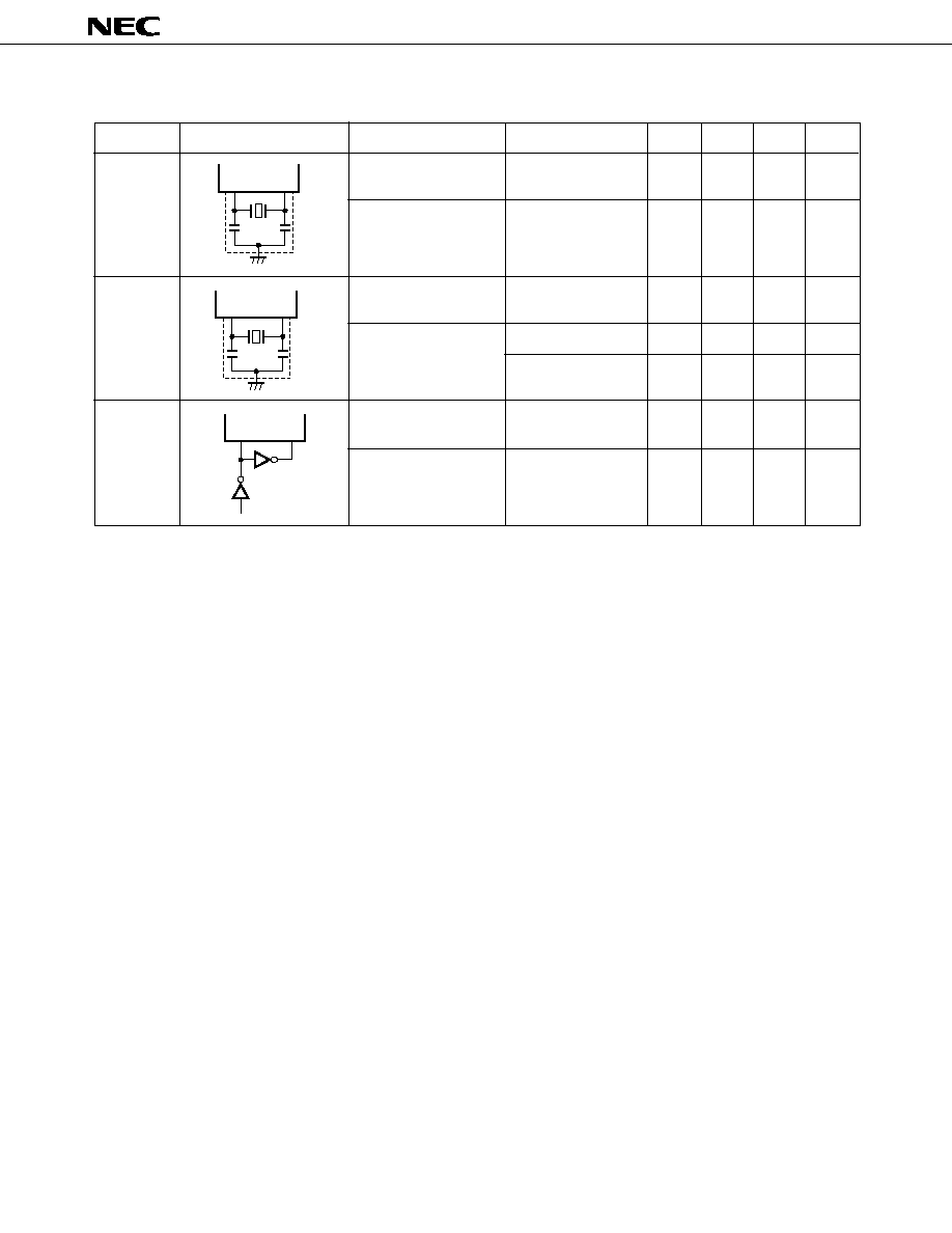
48
µ
PD75212A
X1
X2
C1
C2
X1
X2
C1
C2
MAIN SYSTEM CLOCK OSCILLATOR CHARACTERISTICS (Ta = 40 to +85
°
C, V
DD
= 2.7 to 6.0 V )
V
DD
= Oscillation
voltage range
After V
DD
reaches the
minimum value in
the oscillation
voltage range
V
DD
= 4.5 to 6.0 V
Oscillator frequency
(f
XX
) *2
Oscillation
stabilization time *3
Oscillator frequency
(f
XX
) *2
Oscillation stabilization
time *3
X1 input frequency
(f
X
) *2
X1 input high and low
level widths (t
XH
, t
XL
)
X1
X2
µ
PD74HCU04
2.0
2.0
2.0
100
4.19
5.0 *4
4
5.0 *4
10
30
5.0 *4
250
MHz
ms
MHz
ms
ms
MHz
ns
MIN.
TYP.
MAX.
UNIT
TEST CONDITIONS
PARAMETER
RECOMMENDED CIRCUIT
RESONATOR
Ceramic
resonator*1
Crystal
resonator*1
External
clock
*
1. Refer to RECOMMENDED OSCILLATOR CONSTANTS.
2. Oscillator characteristics only. Refer to the description of AC characteristics for details of instruction execution
time.
3. Time required for oscillation to become stabilized after V
DD
reaches the minimum value in the oscillation
voltage range or STOP mode release.
4. When oscillator frequency is "4.19 < f
XX
<
5.0 MHz", do not select "PCC = 0011" as instruction execution time.
If "PCC = 0011" is selected, 1 machine cycle becomes less than 0.95
µ
s, with the result that the specified MIN.
value of 0.95
µ
s cannot be observed.
Note
When the main system clock oscillator is used, the following should be noted concerning wiring in the area
in the figure enclosed by a dotted line to prevent the influence of wiring capacitance, etc.
· The wiring should be kept as short as possible.
· No other signal lines should be crossed. Keep away from lines carrying a high fluctuating current.
· The oscillator capacitor grounding point should always be at the same potential as V
SS
. Do not connect
to a ground pattern carrying a high current.
· A signal should not be taken from the oscillator.
5
49
µ
PD75212A
XT1
XT2
C3
C4
R
SUBSYSTEM CLOCK OSCILLATOR CHARACTERISTICS (Ta = 40 to +85
°
C, V
DD
= 2.7 to 6.0 V)
Oscillator frequency
(f
XT
) *2
Oscillation stabilization
time *3
XT1 input frequency
(f
XT
)
XT1 input high and low
level widths (t
XTH
, t
XTL
)
V
DD
= 4.5 to 6.0 V
32.768
1.0
35
2
10
100
32
kHz
s
s
kHz
µ
s
Crystal
resonator*1
External
clock
32
32
10
MIN.
TYP.
MAX.
UNIT
TEST CONDITIONS
PARAMETER
RECOMMENDED CIRCUIT
RESONATOR
*
1. Recommended resonators are shown in following page.
2. Oscillator characteristics only. Refer to the description of AC characteristics for instruction execution time.
3. Oscillation stabilization time is a time required for oscillation to become stabilized after V
DD
reaches the
minimum value in the oscillation voltage range.
Note
When the subsystem clock oscillator is used, the following should be noted concerning wiring in the area
in the figure enclosed by a dotted line to prevent the influence of wiring capacitance, etc.
· The wiring should be kept as short as possible.
· No other signal lines should be crossed. Keep away from lines carrying a high fluctuating current.
· The oscillator capacitor grounding point should always be at the same potential as V
SS
. Do not connect
to a ground pattern carrying a high current.
· A signal should not be taken from the oscillator.
The subsystem clock oscillator is a low-amplitude circuit in order to achieve a low consumption current,
and is more prone to misoperation due to noise than the main system clock oscillator. Particular care is
therefore required with the wiring method when the subsystem clock is used.
XT1
Leave Open
XT2
5
50
µ
PD75212A
CSA 2.00MG
CSA 4.19MG
CSA 4.91MG
CAT 2.00MG
CST 4.19MG
CST 4.91MG
KBR2.0MS
KBR4.0MS
KBR4.19MS
KBR4.19MS
FCR 3.58M2
FCR 4.00M2
FCR 4.19M2
FCR 4.19MC
C1
C2
MIN.
MAX.
30
30
EXTERNAL
CAPACITANCE (pF)
OSCILLATION
VOLTAGE RANGE (V)
MANUFACTURER
PRODUCT NAME
REMARKS
RECOMMENDED OSCILLATOR CONSTANTS
MAIN SYSTEM CLOCK : CERAMIC OSCILLATOR (Ta = 40 to +85
°
C)
Not required
47
33
30
Not required
Not required
47
33
30
Not required
4.0
4.0
6.0
6.0
6.0
4.0
On-chip C type
On-chip C type
Murata Mfg. Co., Ltd.
Kyocera Corp.
TDK
MAIN SYSTEM CLOCK : CRYSTAL RESONATOR (Ta = 40 to +85
°
C)
C1
C2
MIN.
MAX.
EXTERNAL
CAPACITANCE (pF)
OSCILLATION
VOLTAGE RANGE (V)
LOAD
CAPACITANCE
CL (pF)
2.00
4.19
4.91
Kinseki
HC18/U
HC49/U
HC-43/U
16
20
20
4.0
6.0
MANUFACTURER
REMARKS
FREQUENCY
(MHz)
HOLDER
EXTERNAL
CAPACITANCE (pF)
C4
(pF)
R
(k
)
MIN.
(V)
MAX.
(V)
OSCILLATION
VOLTAGE RANGE (V)
SUBSYSTEM CLOCK : 32.768 kHz CRYSTAL RESONATOR (Ta = 10 to +60
°
C)
C3
(pF)
P3
CFS308
Kinseki
Citizen Watch Co.
12
14
22
22
22
33
330
330
2.7
6.0
MANUFACTURER
REMARKS
LOAD
CAPACITANCE
CL (pF)
MODEL
NAME
Note
Carry out fine adjustment of crystal oscillator frequency on the external capacitance C1.
Note
Carry out fine adjustment of crystal oscillator frequency on the external capacitance C3.
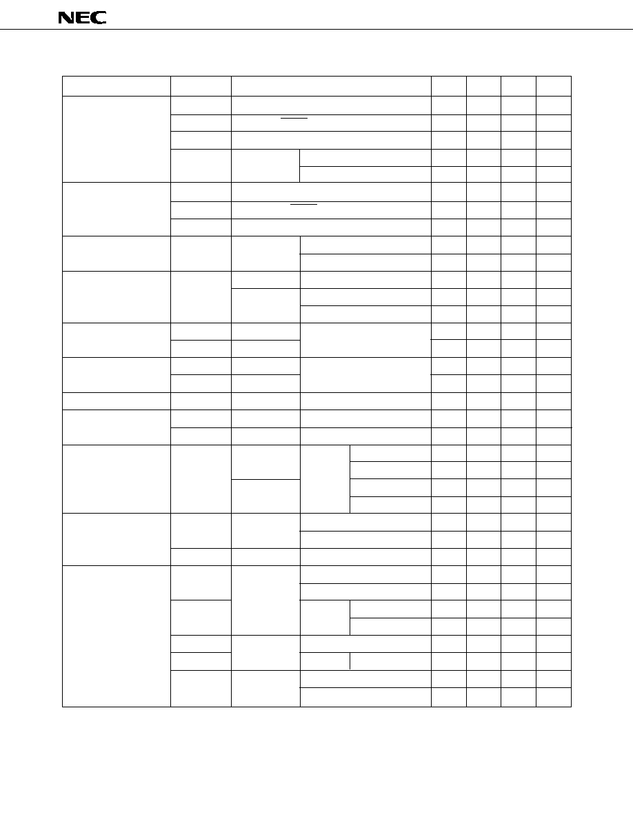
51
µ
PD75212A
0.7 V
DD
0.75 V
DD
V
DD
0.4
0.65 V
DD
0.7 V
DD
0
0
0
V
DD
1.0
V
DD
0.5
3
1.5
15
7
20
20
25
V
V
V
V
V
V
V
V
V
V
V
V
V
µ
A
µ
A
µ
A
µ
A
µ
A
µ
A
µ
A
mA
mA
mA
mA
k
k
k
mA
mA
µ
A
µ
A
µ
A
µ
A
µ
A
µ
A
0.4
5.5
3.5
22
15
80
70
3.0
0.55
600
200
40
5
0.5
0.1
V
IH1
V
IH2
V
IH3
V
IL1
V
IL2
V
IL3
V
OL
I
LIH1
I
LIH2
I
LIL1
I
LIL2
I
LOH
I
LOL1
I
LOL2
All output pins
Display output
Except display output
X1, X2, XT1
X1, X2, XT1
V
DD
= 4.5 to 6.0 V, I
OH
= 1 mA
V
DD
= 4.5 to 6.0 V, I
OL
= 15 mA
V
DD
= 4.5 to 6.0 V, I
OL
= 1.6 mA
All output pins
Except below
Ports 0, 1, 6, RESET
X1, X2, XT1
Except below
Ports 0, 1, RESET
X1, X2, XT1
DC CHARACTERISTICS (Ta = 40 to 85
°
C, V
DD
= 2.7 to 6.0 V)
PARAMETER
SYMBOL
TEST CONDITIONS
Port 6
V
IH4
Input voltage high
Input Voltage low
V
DD
= 4.5 to 6.0 V
I
OH
= 100
µ
A
Output voltage high
V
OH
Ports 4, 5
I
OL
= 400
µ
A
All output pins
Except X1,X2,XT1
Except X1,X2,XT1
Output voltage low
Input leakage current
high
S0 to S9
T0 to T15
V
IN
= V
DD
V
IN
= 0 V
V
OUT
= V
DD
V
OUT
= 0 V
V
OUT
= V
LOAD
= V
DD
35 V
V
DD
=
4.5 to 6.0 V
V
OD
=
V
DD
2 V
V
PRE
= V
DD
9
±
1 V*1
V
PRE
= 0 V
V
PRE
= 0 V
V
PRE
= V
DD
9
±
1 V*1
Port 6
V
IN
= V
DD
V
DD
= 4.5 to 6.0 V
Display output
V
OD
V
LOAD
= 35 V
V
DD
= 5 V
±
10 %*3
V
DD
= 3 V
±
10 %*4
V
DD
= 5 V
±
10 %
V
DD
= 3 V
±
10 %
V
DD
= 3 V
±
10 %
HALT mode
HALT mode V
DD
= 3 V
±
10 %
V
DD
= 5 V
±
10 %
V
DD
= 3 V
±
10 %
4.19 MHz
crystal
oscillation
C1 = C2 =
15 pF
32 kHz crystal
oscillation*5
XT1 = 0 V
STOP mode
I
DD5
I
DD4
I
DD3
I
DD2
I
DD1
R
L
R
P6
I
OD
Input leakage current
low
Output leakage current high
Output leakage current
low
Display output current
Built-in pull-down
resistor (mask option)
Supply current*2
MIN.
TYP.
V
DD
V
DD
V
DD
V
DD
V
DD
0.3 V
DD
0.2 V
DD
0.4
2.0
0.4
0.5
3
20
3
20
3
3
10
200
1000
135
9.0
1.5
1800
600
120
15
20
10
MAX.
UNIT
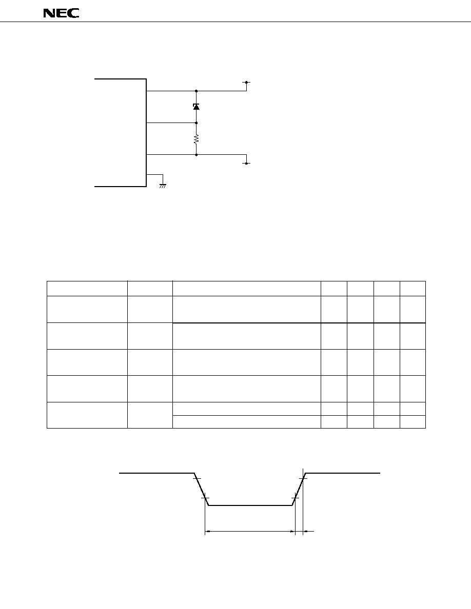
52
µ
PD75212A
*
1. The following external circuit is recommended.
2. Current to the on-chip pull-down resistor and power-on reset circuit (mask option) is not included.
3. When the processor clock control register (PCC) is set to 0011 and is operated in the high-speed mode.
4. When the PCC register is set to 0000 and is operated in the low-speed mode.
5. When the system clock control register (SCC) is set to 1001 and is operated with the subsystem clock with
main system clock oscillation stopped.
Remarks
Start the power supply smoothly.
µ
PD75212A
POWER-ON RESET CIRCUIT CHARACTERISTICS (MASK OPTION) (Ta = 40 to +85
°
C)
Power-on reset
operating voltage high
Power-on reset
operating voltage low
Power supply voltage
off time
Power supply voltage
rise time
Power-on reset circuit*2
current consumption
V
DDH
t
r
V
DDL
t
off
I
DDPR
V
DD
= 5 V
±
10 %
V
DD
= 2.7 V
PARAMETER
SYMBOL
TEST CONDITIONS
MIN.
TYP.
MAX.
UNIT
4.5
0
10
1
10
2
6.0
0.2
*1
100
20
V
V
µ
s
µ
A
µ
A
s
*
1. 2
17
/f
XX
(31.3 ms at f
XX
= 4.19 MHz)
2. Current with on-chip power-on reset circuit or power-on flag.
V
DD
V
DDH
V
DDL
t
r
t
off
V
DD
V
PRE
V
LOAD
V
SS
RD9, 1EL
68 k
+5 V
30 V
RD9, 1EL :Zener Diode (NEC)
Zener Voltage = 8.29 to 9.30 V
53
µ
PD75212A
Input
Output
Input
Output
AC CHARACTERISTICS (Ta = 40 to +85
°
C , V
DD
= 2.7 to 6.0 V)
PARAMETER
SYMBOL
TEST CONDITIONS
MIN.
TYP.
MAX.
UNIT
Operation with main
system clock
Operation with sub-
system clock
t
CY
CPU clock cycle time
(minimum instruction
execution time = 1
machine cycle) *1
TI0 input frequency
V
DD
= 4.5 to 6.0 V
TI0 input high and low-
level widths
f
TI
V
DD
= 4.5 to 6.0 V
Input
Output
Input
Output
V
DD
= 4.5 to 6.0 V
V
DD
= 4.5 to 6.0 V
V
DD
= 4.5 to 6.0 V
V
DD
= 4.5 to 6.0 V
INT0
INT1
INT2, 4
t
TIH
,
t
TIL
t
KCY
t
RSL
t
INTH
,
t
INTL
t
KSO
t
KSI
t
SIK
t
KH
,
t
KL
RESET low-level width
Interrupt input high and
low-level widths
SCK cycle time
SCK high and low-level
widths
SI setup time (to SCK
)
SI hold time (from SCK
)
SO output delay time
from SCK
0.95
3.8
114
0
0
0.83
3
0.8
0.95
3.2
3.8
0.4
t
KCY
/250
1.6
t
KCY
/2150
100
400
*2
2t
CY
10
10
300
1000
122
32
32
125
0.6
165
µ
s
µ
s
µ
s
MHz
kHz
µ
s
µ
s
µ
s
µ
s
µ
s
µ
s
µ
s
ns
µ
s
ns
µ
s
µ
s
µ
s
µ
s
ns
ns
ns
ns
54
µ
PD75212A
*
1. CPU clock (
) cycle time is determined by the
oscillator frequency of the connected resonator,
the system clock control register (SCC) and the
processor clock control register (PCC). The cycle
time t
CY
characteristics for power supply voltage
V
DD
when the main system clock is in operation is
shown below.
2. 2t
CY
or 128/f
XX
is set by interrupt mode register
(IM0) setting.
40
32
30
6
5
4
3
2
1
0.5
0
1
2
3
4
5
6
Operation Guaranteed
Range
t
CY
VS
V
DD
(Main System Clock in Operation)
Power Supply Voltage V
DD
[V]
Cycle Time t
CY
[
µ
s]
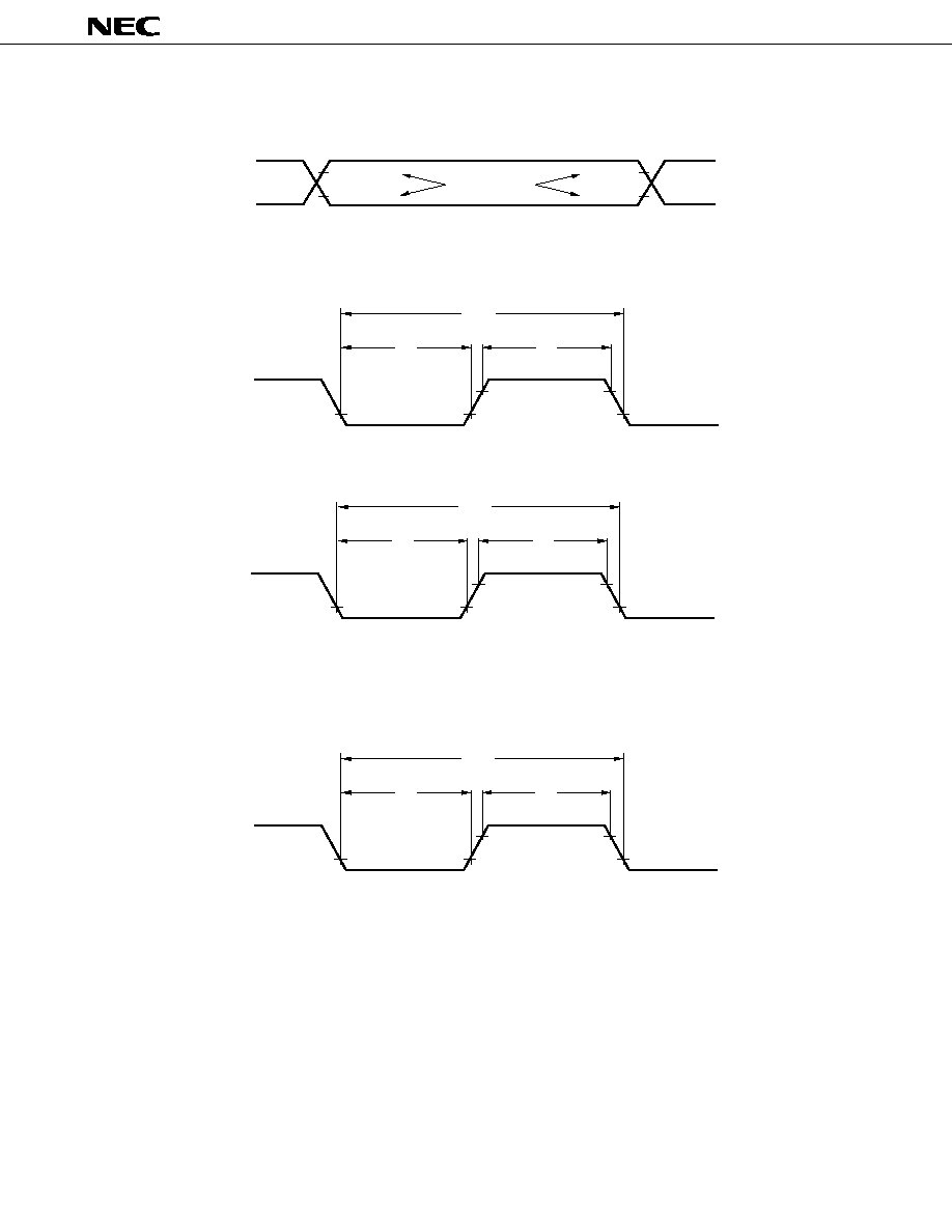
55
µ
PD75212A
1/f
TI
t
TIL
t
TIH
TI0
1/f
XT
t
XTL
t
XTH
V
DD
0.4 V
0.4 V
XT1 Input
1/f
X
t
XL
t
XH
V
DD
0.4 V
0.4 V
X1 Input
AC Timing Test Points (Except X1 and XT1 Inputs)
Clock Timing
TI0 Timing
0.75 V
DD
0.2 V
DD
0.75 V
DD
0.2 V
DD
Test Points
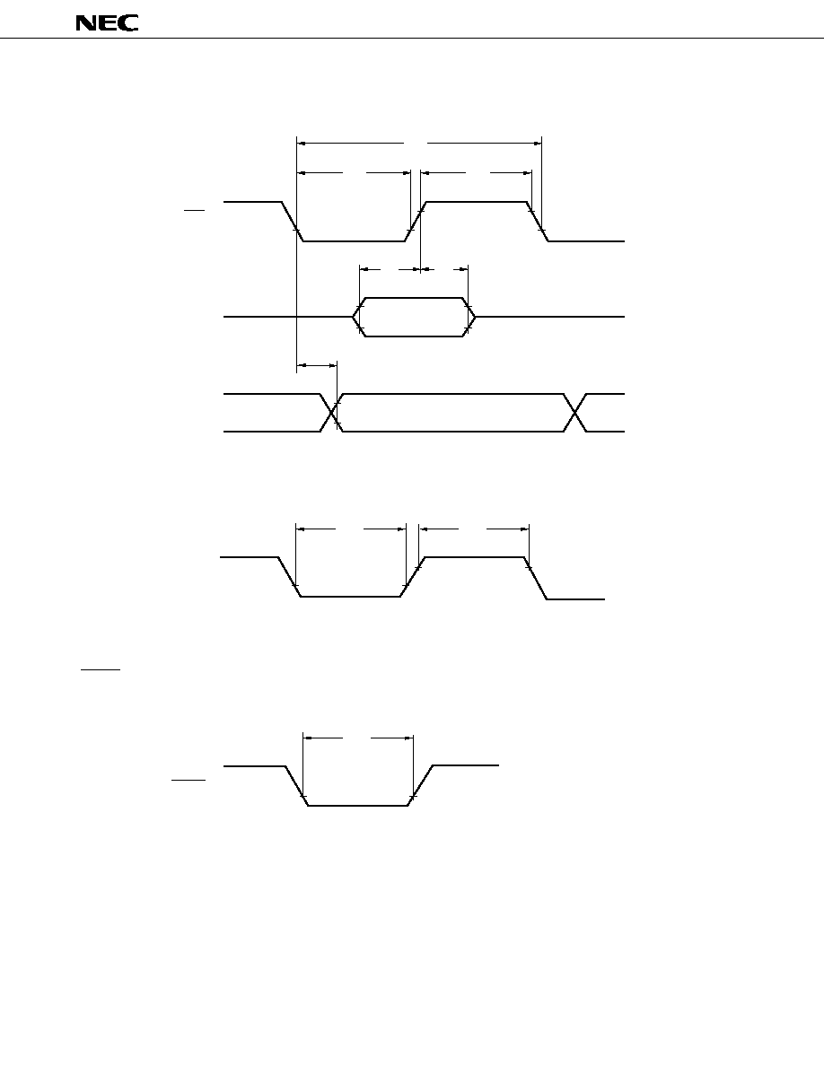
56
µ
PD75212A
Interrupt Input Timing
RESET Input Timing
Serial Transfer Timing
t
KSO
SCK
SI
SO
Input Data
Output Data
t
KCY
t
KH
t
KL
t
SIK
t
KSI
INT0,1,2,4
t
INTL
t
INTH
RESET
t
RSL
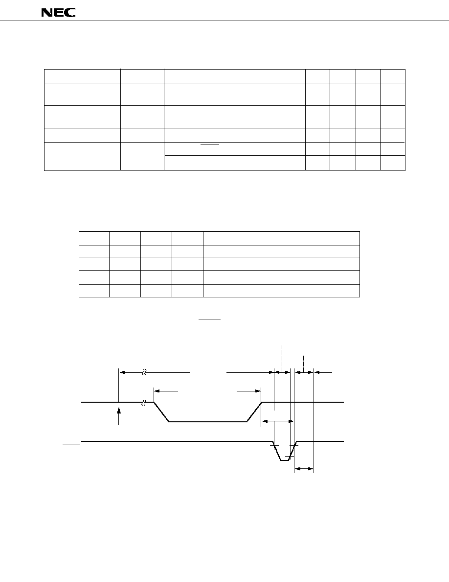
57
µ
PD75212A
2.0
6.0
V
V
DDDR
= 2.0V
0.1
10
µ
A
0
µ
s
Release by RESET
2
17
/f
X
ms
Release by interrupt request
*3
ms
DATA MEMORY STOP MODE LOW POWER SUPPLY VOLTAGE DATA RETENTION CHARACTERISTICS (Ta = 40
to +85
°
C)
PARAMETER
SYMBOL
TEST CONDITIONS
MIN.
TYP.
MAX.
UNIT
Data retention power
supply voltage
Data retention power
supply current *1
t
SREL
t
WAIT
V
DDDR
I
DDDR
Release signal set time
Oscillation stabilization
wait time *2
Data Retention Timing (STOP Mode Release by RESET)
STOP Instruction Execution
V
DD
V
DDDR
Operating Mode
HALT Mode
STOP Mode
Data Retention Mode
t
WAIT
RESET
t
SREL
Internal Reset Operation
BTM3
BTM2
BTM1
BTM0
Wait Time (Values at f
XX
= 4.19 MHz in parentheses)
--
0
0
0
2
20
/f
XX
(approx. 250 ms)
--
0
1
1
2
17
/f
XX
(approx. 31.3 ms)
--
1
0
1
2
15
/f
XX
(approx. 7.82 ms)
--
1
1
1
2
13
/f
XX
(approx. 1.95 ms)
*
1. Current to the on-chip pull-down resistor and power-on reset circuit (mask option) is not included.
2. Oscillation stabilization wait time is time to stop CPU operation to prevent unstable operation upon oscillation
start.
3. According to the setting of the basic interval timer mode register (BTM) (see below).
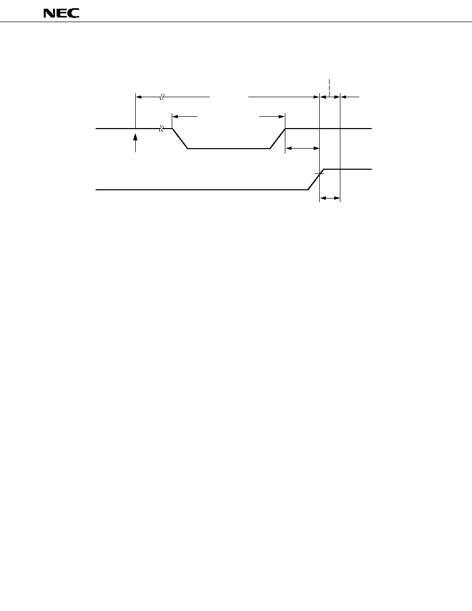
58
µ
PD75212A
Data Retention Timing (Standby Release Signal: STOP Mode Release by Interrupt Signal)
STOP Instruction Execution
V
DD
V
DDDR
Standby Release Signal
(Interrupt Request)
Operating Mode
HALT Mode
STOP Mode
Data Retention Mode
t
WAIT
t
SREL
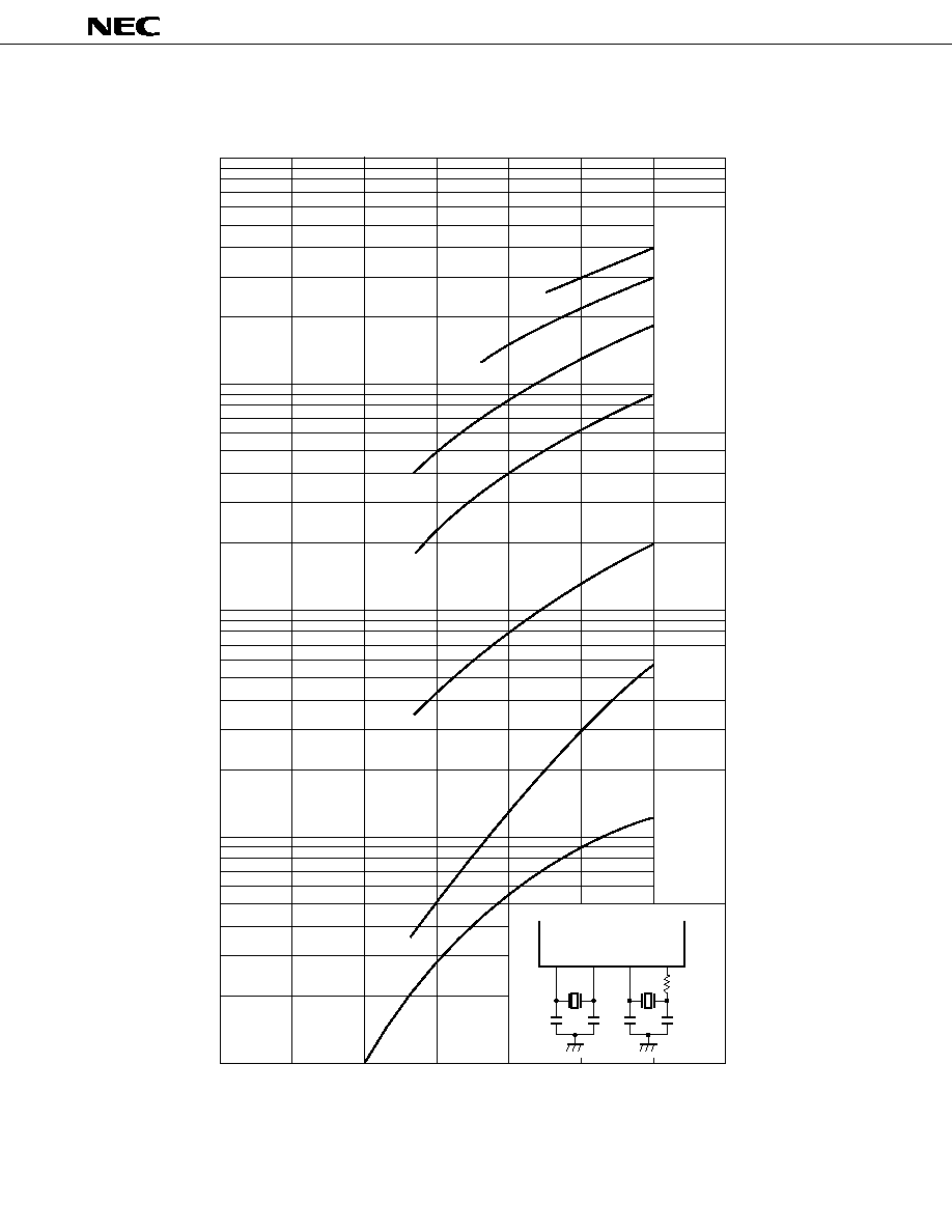
59
µ
PD75212A
13. CHARACTERISTIC CURVES
I
DD
vs V
DD
Supply Voltage V
DD
[V]
Supply Current I
DD
[
µ
A]
Remarks
Values of the processor clock control register (PCC) are indicated in parenthesis.
High-Speed
Mode (0011)
Medium-Speed
Mode (0010)
Low-Speed
Mode (0000)
HALT Mode
(0100)
Subsystem
Clock
Operating
Mode
Subsystem
Clock HALT
Mode
STOP Mode
(1000)
Power-on
reset
circuit and
power-on flag
incorporated
330 k
32.768 kHz
33 pF
22 pF
15 pF
4.19 MHz
15 pF
6
5
4
3
2
1
0
1
10
5
100
50
1000
500
5000
X1
X2
XT1
XT2
(Ta = 25
°
C)
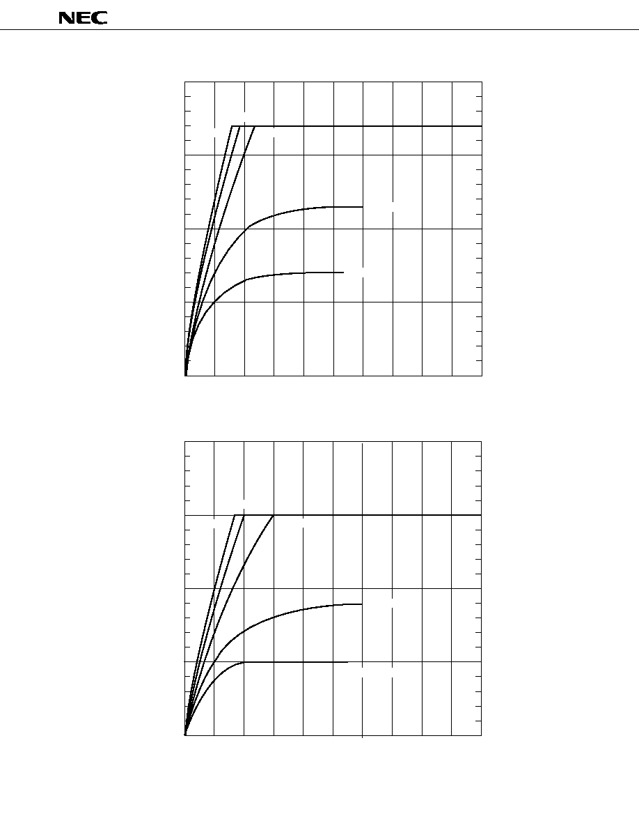
60
µ
PD75212A
I
OL
vs V
OL
(Ports 0, 2, 3, 6)
Output Current Low I
OL
[mA]
Output Voltage Low V
OL
[V]
I
OH
vs (V
DD
V
OH
) (Ports 0, 2, 3, 6)
V
DD
V
OH
[V]
Output Current High I
OH
[mA]
20
15
10
5
0
0
1
2
3
4
5
V
DD
= 6 V
V
DD
= 5 V
V
DD
= 4 V
V
DD
= 3 V
V
DD
= 2.7 V
(Ta = 25 °C)
20
15
10
5
0
0
1
2
3
4
5
V
DD
= 6 V
V
DD
= 5 V
V
DD
= 4 V
V
DD
= 3 V
V
DD
= 2.7 V
(Ta = 25 °C)
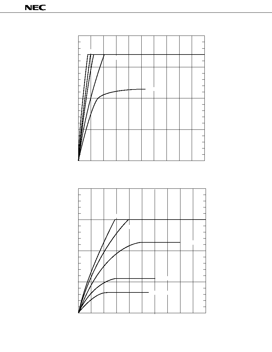
61
µ
PD75212A
I
OL
vs V
OL
(Ports 4, 5)
Output Current Low I
OL
[mA]
Output Voltage Low V
OL
[V]
I
OH
vs (V
DD
V
OH
) (Ports 4, 5)
V
DD
V
OH
[V]
Output Current High I
OH
[mA]
20
15
10
5
0
0
1
2
3
4
5
6 V
V
DD
= 5 V
4 V
V
DD
= 3 V
V
DD
= 2.7 V
(Ta = 25 °C)
20
15
10
5
0
0
1
2
3
4
5
V
DD
= 6 V
V
DD
= 5 V
V
DD
= 4 V
V
DD
= 3 V
V
DD
= 2.7 V
(Ta = 25 °C)
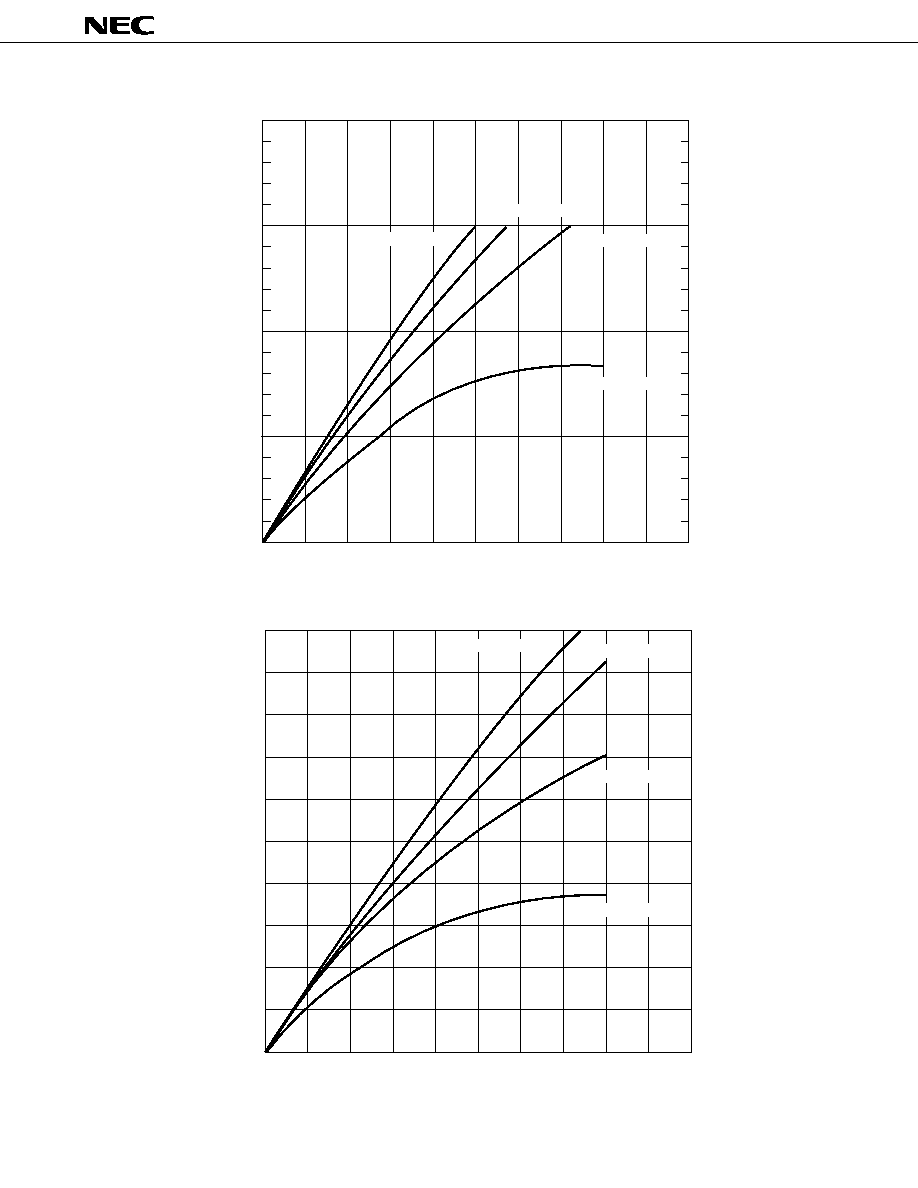
62
µ
PD75212A
40.0
30.0
20.0
10.0
0
0
1
2
3
4
5
(Ta = 25 °C)
V
DD
V
PRE
= 6 V
V
DD
V
PRE
= 8 V
V
DD
V
PRE
= 10 V
V
DD
V
PRE
= 4 V
I
OD
vs (V
DD
to V
OD
) (T0 to T15)
V
DD
V
OD
[V]
Display Output Current I
OD
[mA]
I
OD
vs (V
DD
V
OD
) (S0 to S9)
V
DD
V
OD
[V]
Display Output Current I
OD
[mA]
10.0
5.0
0
0
1
2
3
4
5
(Ta = 25 °C)
V
DD
V
PRE
= 6 V
V
DD
V
PRE
= 8 V
V
DD
V
PRE
= 10 V
V
DD
V
PRE
= 4 V
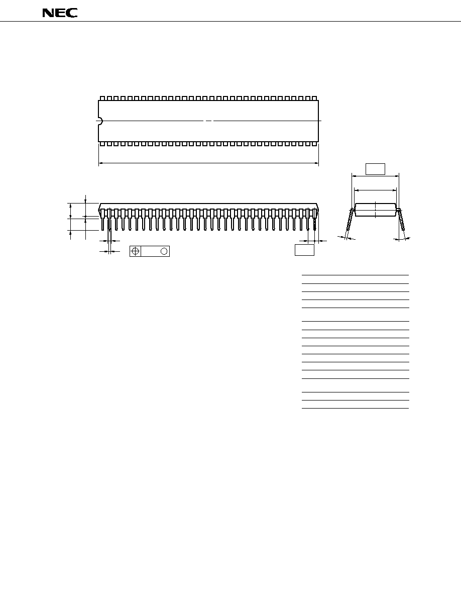
63
µ
PD75212A
14. PACKAGE INFORMATION
A
I
J
G
H
F
D
N
M
C
B
M
R
64
33
32
1
K
L
NOTE
Each lead centerline is located within 0.17 mm (0.007 inch) of
its true position (T.P.) at maximum material condition.
P64C-70-750A,C-1
ITEM MILLIMETERS
INCHES
A
B
C
D
F
G
H
I
J
K
58.68 MAX.
1.778 (T.P.)
3.2±0.3
0.51 MIN.
4.31 MAX.
1.78 MAX.
L
M
0.17
0.25
19.05 (T.P.)
5.08 MAX.
17.0
N
0~15°
0.50±0.10
0.9 MIN.
R
2.311 MAX.
0.070 MAX.
0.020
0.035 MIN.
0.126±0.012
0.020 MIN.
0.170 MAX.
0.200 MAX.
0.750 (T.P.)
0.669
0.010
0.007
0~15°
+0.004
0.003
0.070 (T.P.)
1)
Item "K" to center of leads when formed parallel.
2)
+0.10
0.05
+0.004
0.005
64 PIN PLASTIC SHRINK DIP (750 mil)
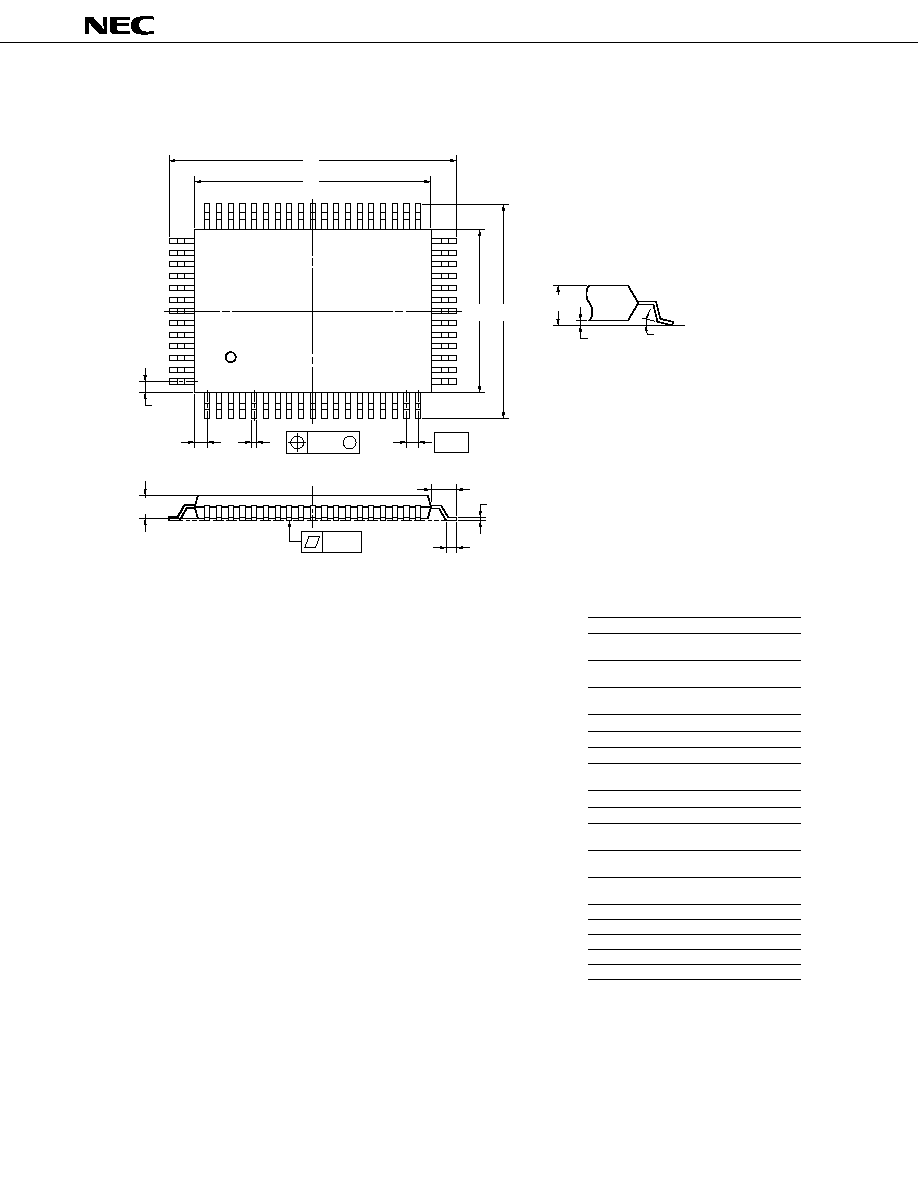
64
µ
PD75212A
64 PIN PLASTIC QFP (14
×
20)
P64GF-100-3B8,3BE,3BR-2
ITEM
MILLIMETERS
INCHES
A
B
C
23.6±0.4
20.0±0.2
14.0±0.2
0.929±0.016
0.795
0.551
D
17.6±0.4
0.693±0.016
F
1.0
0.039
G
1.0
0.039
H
0.40±0.10
0.016
I
0.20
0.008
J
1.0 (T.P.)
0.039 (T.P)
K
1.8±0.2
0.071
L
0.8±0.2
0.031
M
0.15
0.006
N
0.10
0.004
P
2.7
0.106
Q
0.1±0.1
0.004±0.004
R
5°±5°
5°±5°
S
3.0 MAX.
0.119 MAX.
+0.008
0.009
+0.009
0.008
+0.004
0.005
+0.008
0.009
+0.009
0.008
+0.004
0.003
NOTE
Each lead centerline is located within 0.20 mm (0.008 inch) of
its true position (T.P.) at maximum material condition.
51
52
32
64
1
20
19
33
I
J
M
N
H
G
F
A
S
P
K
L
M
B
C
D
detail of lead end
Q
R
+0.10
0.05
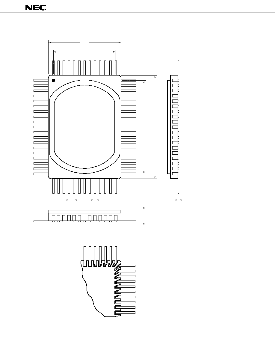
65
µ
PD75212A
64-pin ceramic QFP for ES (reference) (unit : mm)
14.2
12.0
64
52
1
51
32
20
19
33
0.4
1.0
2.25
18.0
0.15
Bottom
View
20
Note
1. Care is needed since the metal cap is con-
nected to pin 26 and set to the positive
power supply level.
2. Care is needed since the lead of the base is
formed obliquely.
3. The lead length is not stipulated since the
cutting of the lead ends is not progress-
controlled.
66
µ
PD75212A
15. RECOMMENDED SOLDERING CONDITIONS
This product should be soldered and mounted under the conditions recommended below.
For details of recommended soldering conditions, refer to the information document "Semiconductor Device
Mount Manual" (IEI-1207).
For soldering methods and conditions other than those recommended below, contact our salesman.
Table 15-1 Surface Mounting Type Conditions
Recommended
Condition Symbol
Soldering Method
Soldering Conditions
Solder bath temperature: 260
°
C or less, Duration: 10 sec. max.
Number of times: Once, Time limit: 7 days* (thereafter 10 hours prebaking required
at 125
°
C)
Preheating temperature : 120
°
C max. (package surface temperature)
Package peak temperature: 230
°
C, Duration: 30 sec. max. (at 210
°
C or above),
Number of times: Once, Time limit: 7 days*(thereafter 10 hours prebaking required
at 125
°
C)
Package peak temperature: 215
°
C, Duration: 40 sec. max. (at 200
°
C or above),
Number of times: Once, Time limit: 7 days* (thereafter 10 hours prebaking required
at 125
°
C)
Pin part temperature: 300
°
C or below , Duration: 3 sec. max. (per device side)
Pin part heating
VPS
Infrared reflow
Wave soldering
VP15-107-1
IR-30-107-1
WS60-107-1
µ
PD75212AGF-
×××
-3BE : 64-pin plastic QFP (14
×
20 mm)
Table 15-2 Insertion Type Soldering Conditions
µ
PD75212ACW-
×××
: 64-pin plastic shrink DIP (750 mil)
Soldering Method
Soldering Conditions
Wave soldering
(lead part only)
Solder bath temperature: 260
°
C or below , Duration: 10 sec. max.
Pin part temperature: 260
°
C or below , Duration: 10 sec. max.
Pin part heating
Note
Ensure that the application of wave soldering is limited to the lead part and no solder touches the main
unit directly.
*
For the storage period after dry-pack decompression storage conditions are max. 25
°
C, 65 % RH.
Note Use of more than one soldering method should be avoided (except in the case of pin part heating).
Notice
A Version of this product with improved recommended soldering condition is available. For details
(improvements such as infrared reflow peak temperature extension (235
°
C), number of times: twice,
relaxation of time limit, etc.), contact NEC sales personnel.
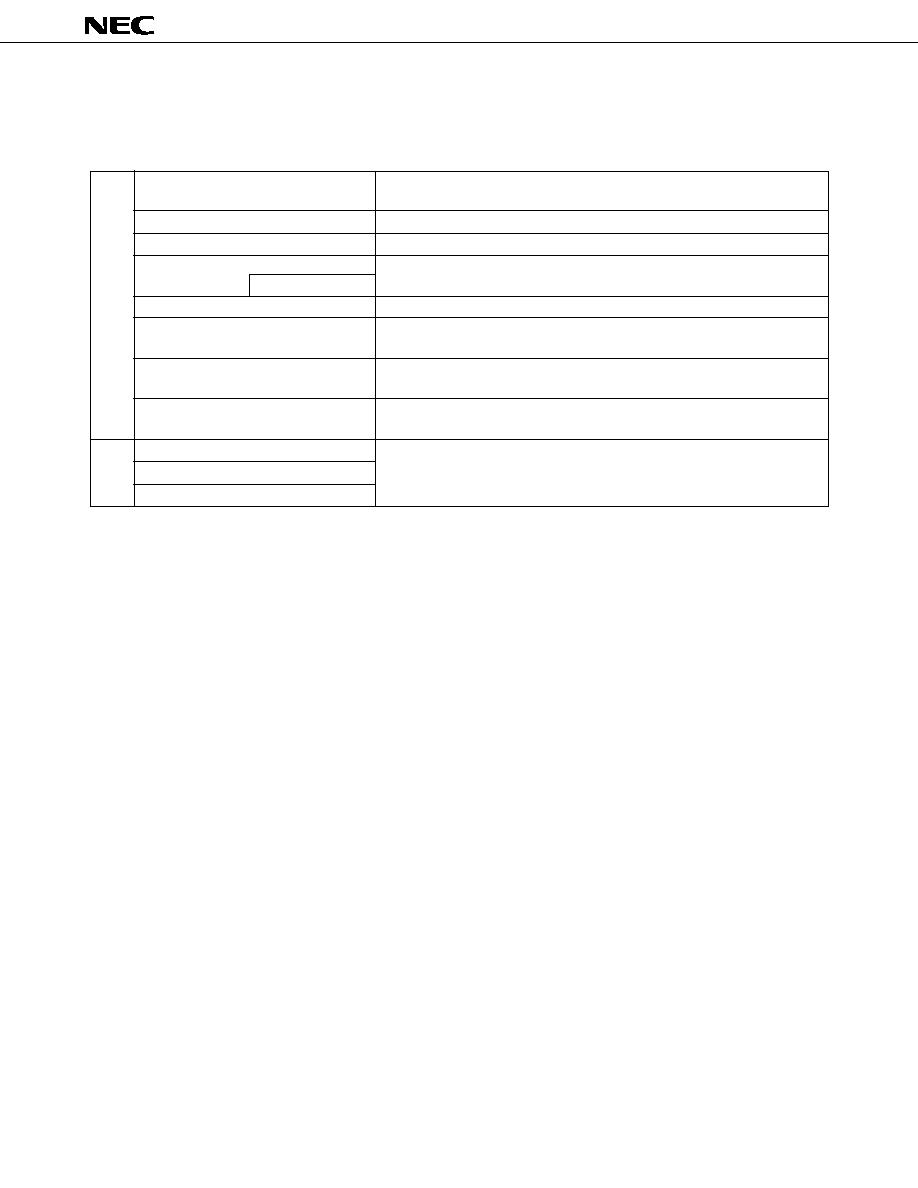
67
µ
PD75212A
APPENDIX A. DEVELOPMENT TOOLS
The following development tools are available for the development of systems using the
µ
PD75212A.
IE-75000-R*1
In-circuit emulator for the 75X series
IE-75001-R
IE-75000-R-EM*2
Emulation board for the IE-75000-R and IE-75001-R
EP-75216ACW-R
Emulation probe for
µ
PD75216ACW
EP-75216AGF-R
Emulation probe for
µ
PD75216AGF provided with the 64-pin conversion
EV-9200G-64
socket EV-9200G-64
PG-1500
PROM programmer
PA-75P216ACW
PROM programmer adapter for
µ
PD75P216ACW/75P218CW in
connection with PG-1500
PA-75P218GF
PROM programmer adapter for
µ
PD75P218GF in connection with
PG-1500
PA-75P218KB
PROM programmer adapter for
µ
PD75P218KB in connection with
PG-1500.
IE control program
Host machine
PG-1500 controller
· PC-9800 series (MS-DOSTM Ver.3.30 to Ver.5.00A*3)
RA75X relocatable assembler
· IBM PC/ATTM (PC DOSTM Ver.3.1)
*
1. Maintenance product
2. Not incorporated in the IE-75001-R
3. The task swap function, which is provided with Ver.5.00/5.00A, is not available with this software.
Remarks
For development tools manufactured by a third party, see the 75X Series Selection Guide (IF-151).
Software
Hardware
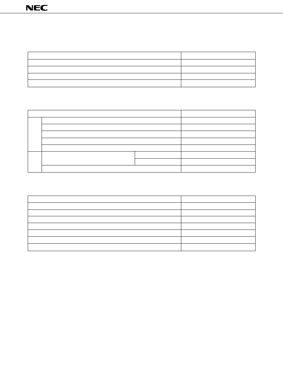
68
µ
PD75212A
APPENDIX B. RELATED DOCUMENTS
Device Related Documents
Document Name
Document No.
User's Manual
Instruction Application Table
Application Note
75X Series Selection Guide
Development Tools Related Documents
Document Name
Document No.
IE-75000-R/IE-75001-R User's Manual
IE-75000-R-EM User's Manual
EP-75216ACW-R User's Manual
EP-75216AGF-R User's Manual
PG-1500 User's Manual
RA75X Assembler Package User's Manual
Operation Volume
Language Volume
PG-1500 Controller User's Manual
Other Documents
Document Name
Document No.
Package Manual
Surface Mount Technology Manual
Quality Grade on NEC Semiconductor Devices
NEC Semiconductor Device Reliability & Quality Control
Electrostatic Discharge (ESD) Test
Semiconductor Devices Quality Guarantee Guide
Microcomputer Related Products Guide Other Manufactures Volume
Note
The contents of the above related documents are subjected to change without notice. The latest documents
should be used for design, etc.
Hardware
Software

69
µ
PD75212A

[MEMO]
[MEMO]
µ
PD75212A
No part of this document may be copied or reproduced in any form or by any means without the prior written
consent of NEC Corporation. NEC Corporation assumes no responsibility for any errors which may appear in this
document.
NEC Corporation does not assume any liability for infringement of patents, copyrights or other intellectual
property rights of third parties by or arising from use of a device described herein or any other liability arising
from use of such device. No license, either express, implied or otherwise, is granted under any patents, copyrights
or other intellectual property rights of NEC Corporation or others.
The devices listed in this document are not suitable for use in aerospace equipment, submarine cables, nuclear
reactor control systems and life support systems. If customers intend to use NEC devices for above applications
or they intend to use "Standard" quality grade NEC devices for applications not intended by NEC, please contact
our sales people in advance.
Application examples recommended by NEC Corporation
Standard :
Computer, Office equipment, Communication equipment, Test and Measurement equipment,
Machine tools, Industrial robots, Audio and Visual equipment, Other consumer products, etc.
Special
:
Automotive and Transportation equipment, Traffic control systems, Antidisaster systems,
Anticrime systems, etc.
M4 92.6
No part of this document may be copied or reproduced in any form or by any means without the prior written
consent of NEC Corporation. NEC Corporation assumes no responsibility for any errors which may appear in this
document.
NEC Corporation does not assume any liability for infringement of patents, copyrights or other intellectual
property rights of third parties by or arising from use of a device described herein or any other liability arising
from use of such device. No license, either express, implied or otherwise, is granted under any patents, copyrights
or other intellectual property rights of NEC Corporation or others.
The devices listed in this document are not suitable for use in aerospace equipment, submarine cables, nuclear
reactor control systems and life support systems. If customers intend to use NEC devices for above applications
or they intend to use "Standard" quality grade NEC devices for applications not intended by NEC, please contact
our sales people in advance.
Application examples recommended by NEC Corporation
Standard :
Computer, Office equipment, Communication equipment, Test and Measurement equipment,
Machine tools, Industrial robots, Audio and Visual equipment, Other consumer products, etc.
Special
:
Automotive and Transportation equipment, Traffic control systems, Antidisaster systems,
Anticrime systems, etc.
EEPROM is a trademark of NEC Corporation.
FIP is a trademark of NEC Corporation.
MS-DOS is a trademark of Microsoft Corporation.
PC DOS, PC/AT are trademarks of IBM Corporation.
Document Outline