 | –≠–ª–µ–∫—Ç—Ä–æ–Ω–Ω—ã–π –∫–æ–º–ø–æ–Ω–µ–Ω—Ç: FA1A4M | –°–∫–∞—á–∞—Ç—å:  PDF PDF  ZIP ZIP |
©
1985
DATA SHEET
SILICON TRANSISTOR
FA1A4M
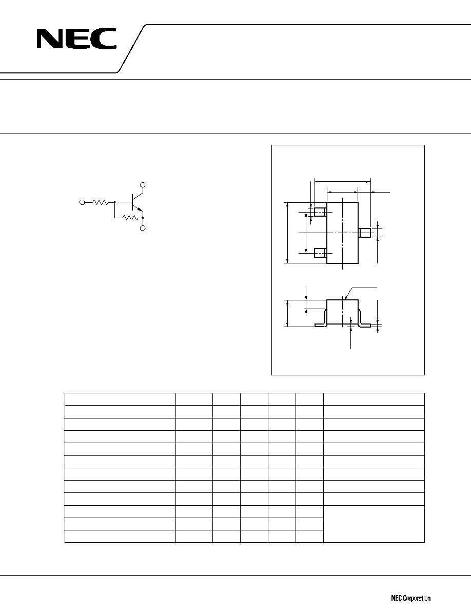
FEATURES
∑
Resistors Built-in TYPE
B
R
1
E
R
2
C
∑
Complementary to FN1A4M
ABSOLUTE MAXIMUM RATINGS (T
A
= 25 ∞C)
Collector to Base Voltage
V
CBO
60
V
Collector to Emitter Voltage
V
CEO
50
V
Emitter to Base Voltage
V
EBO
10
V
Collector Current (DC)
I
C
100
mA
Collector Current (Pulse)
I
C
200
mA
Total Power Dissipation
P
T
200
mW
(T
A
= 25 ∞C)
Junction temperature
T
J
150
∞C
Storage Temperature Range
T
stg
≠55 to +150
∞C
ELECTRICAL CHARACTERISTICS (T
A
= 25 ∞C)
CHARACTERISTIC
SYMBOL
MIN.
TYP.
MAX.
UNIT
TEST CONDITIONS
Collector Cutoff Current
I
CBO
100
nA
V
CB
= 50 V, I
E
= 0
DC Current Gain
h
FE1
*
35
62
100
V
CE
= 5.0 V, I
C
= 5.0 mA
DC Current Gain
h
FE2
*
80
230
V
CE
= 5.0 V, I
C
= 50 mA
Collector Saturation Voltage
V
CE(sat)
*
0.05
0.2
V
I
C
= 5.0 mA, I
B
= 0.25 mA
Low-Level Input Voltage
V
IL
*
1.08
0.8
V
V
CE
= 5.0, I
C
= 100
µ
A
High-Level Input Voltage
V
IH
*
3.0
1.4
V
V
CE
= 0.2 V, I
C
= 5.0 mA
Input Resistor
R
1
7.0
10
13
k
Resistor Ratio
R
1
/R
2
0.9
1.0
1.1
Turn-on Time
t
on
0.06
0.2
µ
s
V
CC
= 5 V, V
in
= 5 V
Storage Time
t
stg
2.0
5.0
µ
s
R
L
= 1 k
Turn-off Time
t
off
2.15
6.0
µ
s
PW = 2
µ
s, Duty Cycle
2 %
* Pulsed: PW = 350
µ
s, Duty Cycle = 2 %
MEDIUM SPEED SWITCHING
RESISTOR BUILT-IN TYPE NPN TRANSISTOR
MINI MOLD
PACKAGE DIMENSIONS
in millimeters
Document No. D10215EJ3V0DS00 (3rd edition)
(Previous No. TC-1654)
Date Published October 1995 P
Printed in Japan
2.8±0.2
1.5
0.65
2.9±0.2
0.95
0.95
2
1
3
0.4
0.4
+0.1
≠0.15
Marking
0.3
0 to 0.1
1.1 to 1.4
0.16
Electrode Connection
1. Emitter
2. Base
3. Collector
Marking : L33
+0.1 ≠0.05
+0.1 ≠0.05
+0.1 ≠0.06
FA1A4M
2
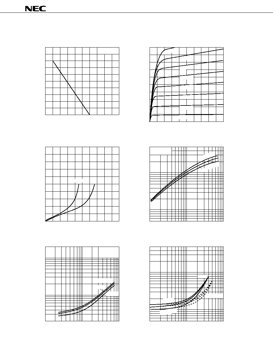
TYPICAL CHARACTERISTICS (T
A
= 25
∞
C)
250
200
150
100
50
50
100
150
200
250
0
T
A
≠ Ambient Temperature ≠ ∞C
P
T
≠ Total Power Dissipation ≠ mW
TOTAL POWER DISSIPATION vs.
AMBIENT TEMPERATURE
Free air
1.0
0.8
0.6
0.4
0.2
20
40
60
80
100
0
I
C
≠ Collector Current ≠ mA
V
CE
≠ Collector to Emitter Voltage ≠ V
COLLECTOR TO EMITTER VOLTAGE vs.
COLLECTOR CURRENT
10 V
V
in
= 5 V
2.0
10
50
5.0
100
1.0
I
C
≠ Collector Current ≠ mA
V
CE(sat)
≠ Collector Saturation Voltage ≠ V
COLLECTOR SATURATION VOLTAGE vs.
COLLECTOR CURRENT
20
T
A
= 75 ∞C
≠25 ∞C
25 ∞C
2.0
1.0
0.5
0.2
0.1
0.05
0.02
I
C
= 10∑I
B
2
4
6
8
10
0
V
CE
≠ Collector to Emitter Voltage ≠ V
I
C
≠ Collector Current ≠ mA
50
40
30
20
10
COLLECTOR CURRENT vs.
COLLECTOR TO EMITTER VOLTAGE
220 A
200 A
180 A
160 A
140 A
120 A
100 A
I
B
= 80 A
DC CURRENT GAIN vs.
COLLECTOR CURRENT
100
I
C
≠ Collector Current ≠ mA
h
FE
≠ DC Current Gain
1.0
2.0
5.0
10
20
50
500
200
100
50
20
10
5
T
A
= 75 ∞C
≠25 ∞C
25 ∞C
V
CE
= 5.0 V
INPUT VOLTAGE vs.
COLLECTOR CURRENT
100
I
C
≠ Collector Current ≠ mA
V
in
≠ Input Voltage ≠ V
1.0
2.0
5.0
10
20
50
50
20
10
5.0
2.0
1.0
0.5
T
A
= 75 ∞C
≠25 ∞C
25 ∞C
V
CE
= 5.0 V
0.2 V
µ
µ
µ
µ
µ
µ
µ
µ
FA1A4M
3
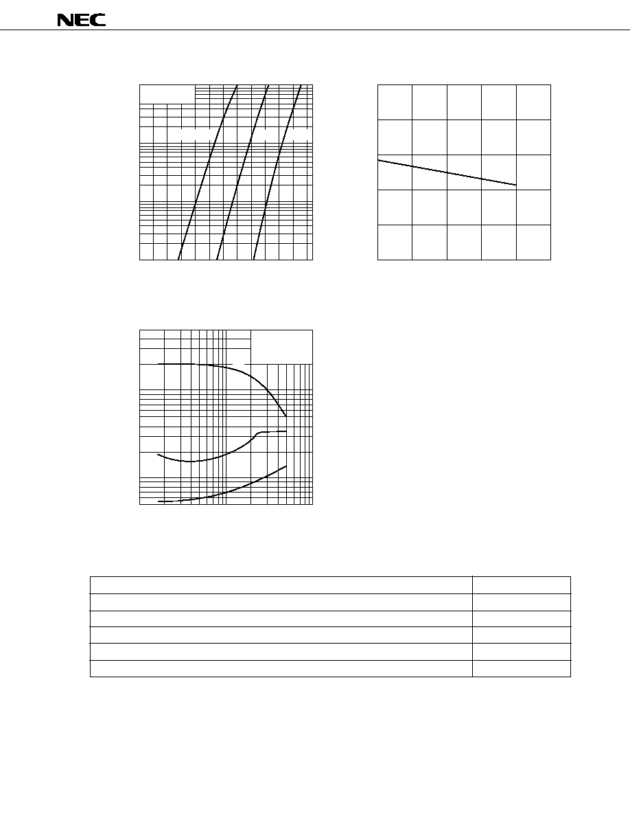
COLLECTOR CURRENT vs.
INPUT VOLTAGE
V
in
≠ Input Voltage ≠ V
I
C
≠ Collector Current ≠ A
1.4
1.2
1.0
0.6
0.4
0.8
1000
100
10
1.0
SWITCHING TIME vs.
COLLECTOR CURRENT
100
I
C
≠ Collector Current ≠ mA
t ≠ Swiching Time ≠ s
1.0
2.0
5.0
10
20
50
5.0
2.0
1.0
0.5
0.2
0.1
0.05
RESISTOR vs.
AMBIENT TEMPERATURE
100
T
A
≠ Ambient Temperature ≠ ∞C
R
1
≠ Resistor ≠ k
≠25
75
50
25
0
20
16
12
8
4
V
in
= 5 V
V
CC
= 5 V
PW = 2 s
Duty Cycle
2 %
t
stg
t
f
t
on
V
CE
= 5.0 V
T
A
= 75 ∞C
≠25 ∞C
25 ∞C
µ
µ
µ
REFERENCE
Document Name
Document No.
NEC semiconductor device reliability/quality control system
TEI-1202
Quality grade on NEC semiconductor devices
IEI-1209
Semiconductor device mounting technology manual
IEI-1207
Guide to quality assurance for semiconductor devices
MEI-1202
Semiconductor selection guide
MF-1134
FA1A4M
No part of this document may be copied or reproduced in any form or by any means without the prior written
consent of NEC Corporation. NEC Corporation assumes no responsibility for any errors which may appear in this
document.
NEC Corporation does not assume any liability for infringement of patents, copyrights or other intellectual
property rights of third parties by or arising from use of a device described herein or any other liability arising
from use of such device. No license, either express, implied or otherwise, is granted under any patents,
copyrights or other intellectual property rights of NEC Corporation or others.
While NEC Corporation has been making continuous effort to enhance the reliability of its semiconductor devices,
the possibility of defects cannot be eliminated entirely. To minimize risks of damage or injury to persons or
property arising from a defect in an NEC semiconductor device, customer must incorporate sufficient safety
measures in its design, such as redundancy, fire-containment, and anti-failure features.
NEC devices are classified into the following three quality grades:
"Standard", "Special", and "Specific". The Specific quality grade applies only to devices developed based on
a customer designated "quality assurance program" for a specific application. The recommended applications
of a device depend on its quality grade, as indicated below. Customers must check the quality grade of each
device before using it in a particular application.
Standard: Computers, office equipment, communications equipment, test and measurement equipment,
audio and visual equipment, home electronic appliances, machine tools, personal electronic
equipment and industrial robots
Special:
Transportation equipment (automobiles, trains, ships, etc.), traffic control systems, anti-disaster
systems, anti-crime systems, safety equipment and medical equipment (not specifically designed
for life support)
Specific: Aircrafts, aerospace equipment, submersible repeaters, nuclear reactor control systems, life
support systems or medical equipment for life support, etc.
The quality grade of NEC devices in "Standard" unless otherwise specified in NEC's Data Sheets or Data Books.
If customers intend to use NEC devices for applications other than those specified for Standard quality grade,
they should contact NEC Sales Representative in advance.
Anti-radioactive design is not implemented in this product.
M4 94.11
[MEMO]