
MDT10P62
This specification are subject to be changed without notice. Any latest information please preview
http;//www.mdtic.com.tw
P.1
2005/6 Ver2.0
1. General Description
This EPROM-Based 8-bit micro-controller uses a fully
static CMOS technology process to achieve higher speed
and smaller size with the low power consumption and high
noise immunity. On chip memory includes 2K words of
ROM, and 128 bytes of static RAM.
2. Features
The followings are some of the features on the hardware
and software :
u
Fully CMOS static design
u
8-bit data bus
u
On chip EPROM size : 2.0 K words
u
Internal RAM size : 160 bytes
(128 general purpose registers, 32 special
registers)
u
37 single word instructions
u
14-bit instructions
u
8-level stacks
u
Operating voltage : 2.5 V ~ 5.5 V (PRD Disable)
4.5 V ~ 5.5 V (PRD Enable)
u
Operating frequency : DC ~ 20 MHz
u
The most fast execution time is 200 ns under 20
MHz in all single cycle instructions except the
branch instruction
u
Addressing modes include direct, indirect and
relative addressing modes
u
Power-on Reset
u
Power edge-detector Reset
u
Power range-detector Reset
u
Sleep Mode for power saving
u
Capture,Compare,PWM module
u
Synchronous serial port with SCM
u
7 interrupt sources:
-External INT pin
-TMR0 timer,TMR1 timer,TMR2 timer
-PortB<7:4> interrupt on change
-CCP,SCM
u
TMR0 : 8-bit real time clock/counter
TMR1 : 16-bit real time clock/count
TMR2 : 8-bit clock/counter(internal)
u
4 types of oscillator can be selected by
programming option:
RC
Low cost RC oscillator
LFXT
Low frequency crystal oscillator
XTAL
Standard crystal oscillator
HFXT
High frequency crystal oscillator
u
On-chip RC oscillator based Watchdog
Timer(WDT)
u
22 I/O pins with their own independent direction
control
3. Applications
The application areas of this MDT10P62 range from
appliance motor control and high speed auto-motive to
low power remote transmitters/receivers, pointing
devices, and telecommunications processors, such as
Remote controller, small instruments, chargers, toy,
automobile and PC peripheral ... etc.
MDT10P62
This specification are subject to be changed without notice. Any latest information please preview
http;//www.mdtic.com.tw
P.2
2005/6 Ver2.0
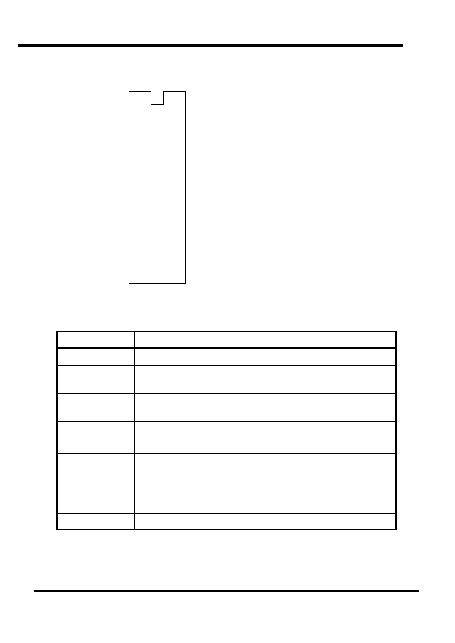
4. Pin Assignment
/MCLR 1
28 PB7
PA0 2
27 PB6
PA1 3
26 PB5
PA2 4
25 PB4
PA3 5
24 PB3
PA4/RTCC 6
23 PB2
PA5/SS 7
22 PB1
V
ss
8
21 PB0/INT
OSC1/CLKIN 9
20 V
dd
OSC2/CLKOUT 10
19 V
ss
PC0/T1OSO/T1CKI 11
18 PC7
PC1/T1OSI 12
17 PC6
PC2/CCP 13
16 PC5/SDO
PC3/SCK 14
15 PC4/SDI
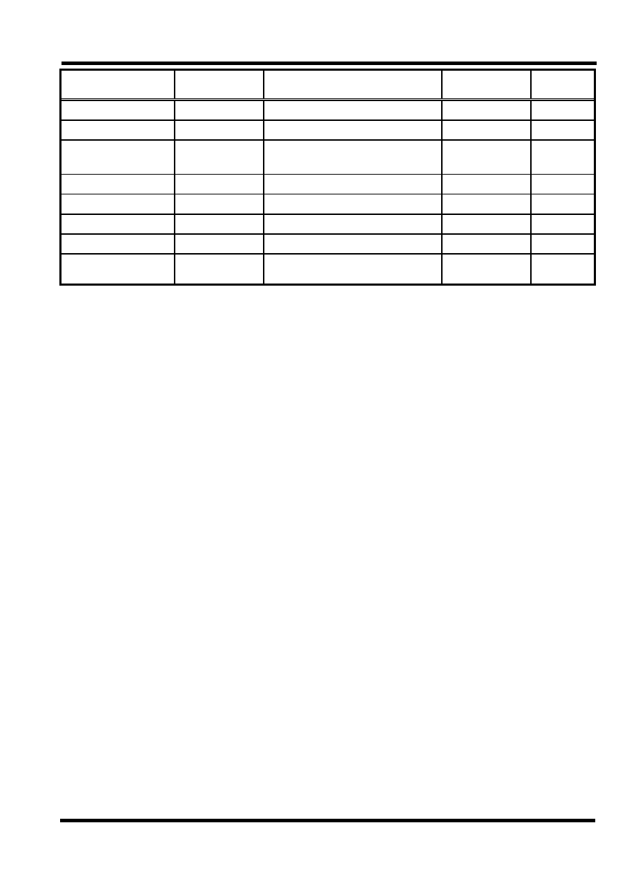
5. Pin Function Description
Pin Name
I/O
Function Description
PA0~PA3,PA5
I/O
Port A, TTL input level
RTCC/PA4
I/O
Real Time Clock/Counter, Schmitt Trigger input levels
Open drain output
PB0~PB7
I/O
Port B, TTL input level / PB0:External interrupt input ,
PB4~PB7:Interrupt on pin change
PC0~PC7
I/O
Port C, Schmitt Trigger input levels
/MCLR
I
Master Clear, Schmitt Trigger input levels
OSC1/CLKIN
I
Oscillator Input/external clock input
OSC2/CLKOUT
O
Oscillator Output/in RC mode
the CLKOUT pin has 1/4 frequency
of CLKIN
V
dd
Power supply
V
ss
Ground

MDT10P62
This specification are subject to be changed without notice. Any latest information please preview
http;//www.mdtic.com.tw
P.3
2005/5 Ver. 1.9
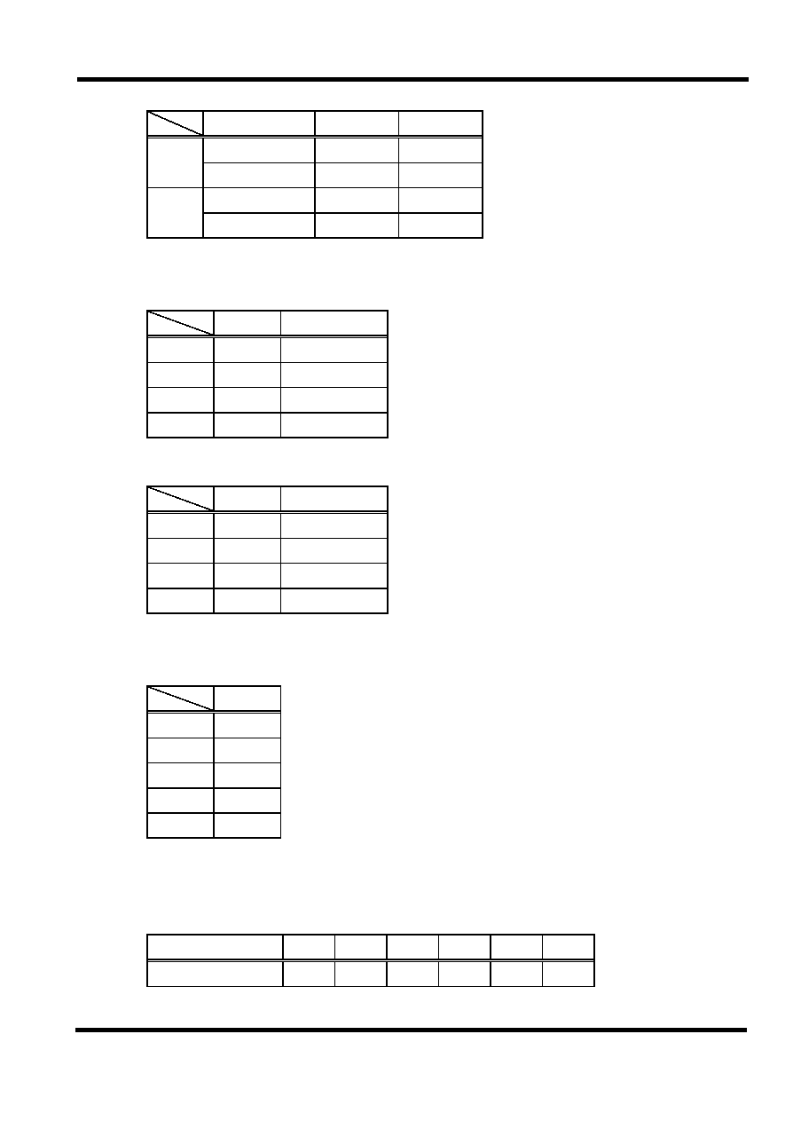
6. Memory Map
(A) Register Map
Address
Description
BANK0
00
Indirect Addressing Register
01
RTCC
02
PCL
03
STATUS
04
MSR
05
Port A
06
Port B
07
Port C
0A
PCHLAT
0B
INTS
0C
PIFB1
0E
TMR1L
0F
TMR1H
10
T1STA
11
TMR2
12
T2STA
13
SCMBUF
14
SCMCTL
15
CCPL
16
CCPH
17
CCPCTL
20~7F
General purpose register
BANK1
01
TMR
05
CPIO A
06
CPIO B
07
CPIO C
0C
PIEB1
MDT10P62
This specification are subject to be changed without notice. Any latest information please preview
http;//www.mdtic.com.tw
P.4
2005/5 Ver. 1.9
Address
Description
0E
PSTA
12
T2PER
14
SCMSTA
A0~BF
General purpose register
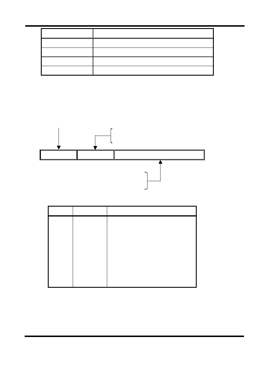
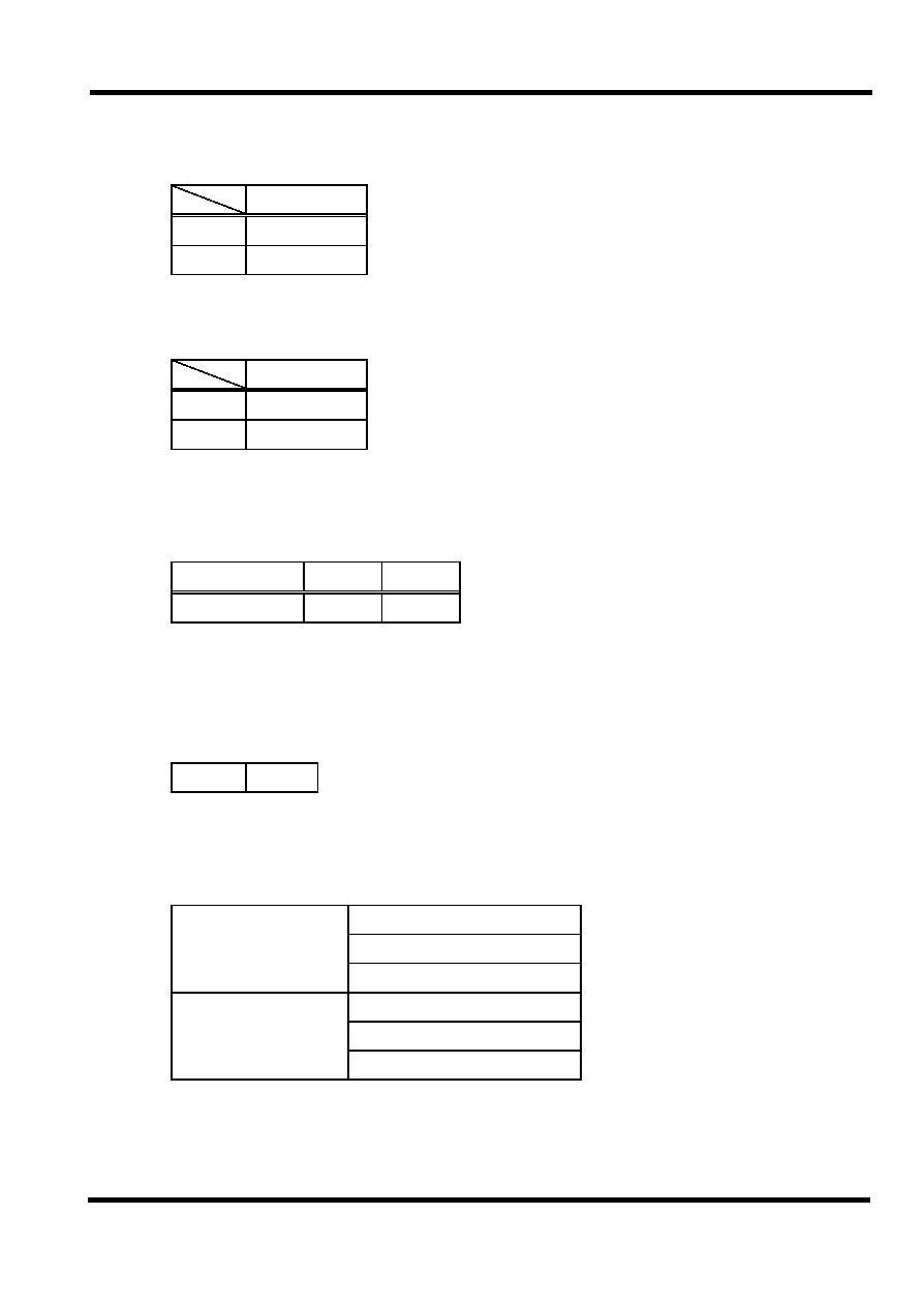
(1)IAR ( Indirect Address Register) : R00
(2)RTCC (Real Time Counter/Counter Register) : R01
(3) PC (Program Counter) : R02,R0A
Write PC --- from PCHLAT
Write PC --- from PCHLAT
LJUMP, LCALL --- from instruction word
RTWI, RET --- from STACK
A11
A10~A8
A7~A0
Write PC --- from ALU
LJUMP, LCALL --- from instruction word
RTWI, RET, RTFI --- from STACK
(4) STATUS (Status register) : R03
Bit
Symbol
Function
0
1
2
3
4
5
6-7
C
HC
Z
PF
TF
RBS0
----
Carry bit
Half Carry bit
Zero bit
Power down Flag bit
WDT Timer overflow Flag bit
Register Bank Select bit :
0 : 00H --- 7FH (Bank0)
1 : 80H --- FFH (Bank1)
General purpose bit
MDT10P62
This specification are subject to be changed without notice. Any latest information please preview
http;//www.mdtic.com.tw
P.5
2005/5 Ver. 1.9
(5) MSR (Memory Bank Select Register) : R04
Memory Bank Select Register :
0 : 00~7F (Bank0)
1 : 80~FF (Bank1)
b7
b6
b5
b4
b3
b2
b1
b0
Indirect Addressing Mode
(6) PORT A : R05
PA5~PA0, I/O Register
(7) PORT B : R06
PB7~PB0, I/O Register
(8) PORT C : R07
PC7~PC0, I/O Register
(9)PCHLAT : R0A
(10) INTS ( Interrupt Status Register ) : R0B
Bit
Symbol
Function
0
RBIF
PORT B change interrupt flag. Set when PB <7:4> inputs change
1
INTF
Set when INT interrupt occurs. INT interrupt flag.
2
TIF
Set when TMR0 overflows.
3
RBIE
0 : disable PB change interrupt
1 : enable PB change interrupt
4
INTS
0 : disable INT interrupt
1 : enable INT interrupt
5
TIS
0 : disable TMR0 interrupt
1 : enable TMR0 interrupt
6
PEIE
0 : disable all peripheral interrupt
1 : enable all peripheral interrupt
7
GIS
0 : disable global interrupt
1 : enable global interrupt

MDT10P62
This specification are subject to be changed without notice. Any latest information please preview
http;//www.mdtic.com.tw
P.6
2005/5 Ver. 1.9
(11)PIFB1 (Peripheral Interrupt Flag Bit) : R0C
Bit
Symbol
Function
0
TMR1IF
TMR1 interrupt flag
0 : TMR1 did not overflow
1 : TMR1 overflowed
1
TMR2IF
TMR2 interrupt flag
0 : No TMR2 to T2PER match occurred
1 : TMR2 to T2PER match occurred
2
CCPIF
CCP interrupt flag
0 : No TMR1 capture/compare occurred
1 : A TMR1 capture/compare occurred
3
SCMIF
SCM interrupt flag
0 : Waiting SCM transmit/receive
1 : The SCM transmission/reception is complete
7~4
--
Unimplemented
(12) TMR1L : R0E
The LSB of the 16-bit TMR1
(13) TMR1H : R0F
The MSB of the 16-bit TMR1
(14) T1STA : R10
Bit
Symbol
Function
0
TMR1ON 0 : Stop TMR1
1 : enable TMR1
1
TMR1CLK 0 : Internal clock (Fosc/4)
1 : External clock from pin PC0
2
/T1SYNC TMR1CLK = 1
0 : Synchronize external clock
1 : Do not synchronize external clock
TMR1CLK = 0
This bit is ignored
3
T1OSCEN 0 : TMR1 Oscillator is shut off
1 : TMR1 Oscillator is enable

MDT10P62
This specification are subject to be changed without notice. Any latest information please preview
http;//www.mdtic.com.tw
P.7
2005/5 Ver. 1.9
Bit
Symbol
Function
5~4
T1CKPS1
~
T1CKPS0
1 1 = 1:8 Prescale value
1 0 = 1:4 Prescale value
0 1 = 1:2 Prescale value
0 0 = 1:1 Prescale value
7~6
--
Unimplemented
(15) TMR2 : R11
TMR2 register
(16) T2STA : R12
Bit
Symbol
Function
1~0
T2CKPS1
~
T2CKPS0
0 0 = Prescaler is 1
0 1 = Prescaler is 4
1 x = Prescaler is 16
2
TMR2ON 0 : TMR2 is on
1 : TMR2 is off
7~3
--
Unimplemented
(17) SCMBUF : R13
Serial communication port buffer
(18) SCMCTL : R14
Bit
Symbol
Function
3~0
SCM3
~
SCM0
0 0 0 0 : SCM master mode , clock = Fosc/4
0 0 0 1 : SCM master mode , clock = Fosc/16
0 0 1 0 : SCM master mode , clock = Fosc/64
0 0 1 1 : SCM master mode , clock = TMR2 output/2
0 1 0 0 : SCM slave mode , clock = SCK pin , /SS control enable
0 1 0 1 : SCM slave mode , clock = SCK pin , /SS control disable
4
CKS
0 : Transmit happens on rising edge , receive on falling edge, Idle state for
clock is low level
1 : Transmit happens on falling edge , receive on rising edge, Idle state for
clock is high level.

MDT10P62
This specification are subject to be changed without notice. Any latest information please preview
http;//www.mdtic.com.tw
P.8
2005/5 Ver. 1.9
Bit
Symbol
Function
5
SCMEN
0 : disable SCM, then pc3, pc4, pc5 is I/O port
1 : enable SCM
6
SCMROI
0 : No overflow
1 : Overflow
7
WCOL
0 : No collision
1 : The SCMBUF is written while it is still transmitting the previous word
(19) CCPL : R15
Capture/Compare/PWM LSB
(20) CCPH : R16
Capture/Compare/PWM MSB
(21) CCPCTL : R17
Bit
Symbol
Function
3~0
CCPM3
~
CCPM0
0 0 0 0 : CCP off
0 1 0 0 : Capture mode , every falling edge
0 1 0 1 : Capture mode , every rising edge
0 1 1 0 : Capture mode , every 4
th
rising edge
0 1 1 1 : Capture mode , every 16
th
rising edge
1 0 0 0 : Compare mode , set output on match
1 0 0 1 : Compare mode , clear output on match
1 0 1 0 : Compare mode , generate software interrupt on match
1 0 1 1 : Compare mode , trigger special event
1 1 x x : PWM mode
5~4
PWMLSB These bits are the two LSBs of the PWM duty cycle
7~6
--
Unimplemented

MDT10P62
This specification are subject to be changed without notice. Any latest information please preview
http;//www.mdtic.com.tw
P.9
2005/5 Ver. 1.9
(22) TMR (Time Mode Register) : R81
Bit
Symbol
Function
Prescaler Value
RTCC rate
WDT rate
2~0
PS2~0
0 0 0
0 0 1
0 1 0
0 1 1
1 0 0
1 0 1
1 1 0
1 1 1
1 : 2
1 : 4
1 : 8
1 : 16
1 : 32
1 : 64
1 : 128
1 : 256
1 : 1
1 : 2
1 : 4
1 : 8
1 : 16
1 : 32
1 : 64
1 : 128
3
PSC
Prescaler assignment bit :
0
--
RTCC
1
--
Watchdog Timer
4
TCE
RTCC signal Edge :
0
--
Increment on low-to-high transition on RTCC pin
1
--
Increment on high-to-low transition on RTCC pin
5
TCS
RTCC signal set :
0
--
Internal instruction cycle clock
1
--
Transition on RTCC pin
6
IES
Interrupt edge select
0
--
Interrupt on falling edge on PB0
1
--
Interrupt on rising edge on PB0
7
PBPH
PORTB pull-hi
0
--
PORTB pull-hi are enable
1
--
PORTB pull-hi are disable
(23) CPIO A (Control Port I/O Mode Register) : R85
"0", I/O pin in output mode;
"1", I/O pin in input mode.
(24) CPIO B (Control Port I/O Mode Register) : R86
"0", I/O pin in output mode;
"1", I/O pin in input mode.
(25) CPIO C (Control Port I/O Mode Register) : R87
"0", I/O pin in output mode;
"1", I/O pin in input mode.
(26) PIEB1 : R8C
Bit
Symbol
Function
0
TMR1IE
TMR1 interrupt enable bit
0 : disable TMR1 interrupt
1 : enable TMR1 interrupt

MDT10P62
This specification are subject to be changed without notice. Any latest information please preview
http;//www.mdtic.com.tw
P.10
2005/5 Ver. 1.9
Bit
Symbol
Function
1
TMR2IE
TMR2 interrupt enable bit
0 : disable TMR2 interrupt
1 : enable TMR2 interrupt
2
CCPIE
CCP interrupt enable bit
0 : disable CCP interrupt
1 : enable CCP interrupt
3
SCMIE
SCM interrupt enable bit
0 : disable SCM interrupt
1 : enable SCM interrupt
7~4
--
Unimplemented
(27) PSTA : R8E
Bit Symbol
Function
0
PRDB
0:Power range-detector Reset occurred
1:No Power range-detector Reset Occurred
1
PORB
0:Power on Reset occurred
1:No Power on Reset occurred
(28) T2PER : R92
Timer2 period
(29) SCMSTA : R94
Bit
Symbol
Function
0
BF
0 : Receive not complete
1 : Receive complete
7~1
--
Unimplemented
(30) Configurable options for EPROM (Set by writer) :
Oscillator Type
RC Oscillator
HFXT Oscillator
XTAL Oscillator
LFXT Oscillator
MDT10P62
This specification are subject to be changed without notice. Any latest information please preview
http;//www.mdtic.com.tw
P.11
2005/5 Ver. 1.9
Watchdog Timer control
Watchdog timer disable all the time
Watchdog timer enable all the time
Power-range control
Power-range disable
Power-range enable
Oscillator-start Timer control
0ms
75ms
Power-edge Detect
Security state
PED Disable
Security Disable
PED Enable
Security Enable
(B) Program Memory
Address
Description
000-7FF
Program memory
000
The starting address of power on, external reset or WDT time-out reset.
004
Interrupt vector
7. Reset Condition for all Registers
Register
Address
Power-On Reset,
Power range detector Reset
/MCLR or WDT Reset
Wake-up from SLEEP
IAR
00h
N/A
N/A
N/A
RTCC
01h
xxxx xxxx
uuuu uuuu
uuuu uuuu
PC
0Ah,02h
0000 0000 0000
0000 0000 0000
PC+1
STATUS
03h
0001 1xxx
000# #uuu
000# #uuu
MSR
04h
xxxx xxxx
uuuu uuuu
uuuu uuuu
PORT A
05h
--xx xxxx
--uu uuuu
--uu uuuu
PORT B
06h
xxxx xxxx
uuuu uuuu
uuuu uuuu

MDT10P62
This specification are subject to be changed without notice. Any latest information please preview
http;//www.mdtic.com.tw
P.12
2005/5 Ver. 1.9
Register
Address
Power-On Reset,
Power range detector Reset
/MCLR or WDT Reset
Wake-up from SLEEP
PORT C
07h
xxxx xxxx
uuuu uuuu
uuuu uuuu
PCHLAT
0Ah
---0 0000
---0 0000
---u uuuu
INTS
0Bh
0000 000x
0000 000u
uuuu uuuu
PIFB1
0Ch
---- 0000
---- 0000
---- uuuu
TMR1L
0Eh
xxxx xxxx
uuuu uuuu
uuuu uuuu
TMR1H
0Fh
xxxx xxxx
uuuu uuuu
uuuu uuuu
T1STA
10h
--00 0000
--uu uuuu
--uu uuuu
TMR2
11h
0000 0000
0000 0000
uuuu uuuu
T2STA
12h
---- -000
---- -uuu
---- -uuu
SCMBUF
13h
xxxx xxxx
uuuu uuuu
uuuu uuuu
SCMCTL
14h
0000 0000
0000 0000
uuuu uuuu
CCPL
15h
xxxx xxxx
uuuu uuuu
uuuu uuuu
CCPH
16h
xxxx xxxx
uuuu uuuu
uuuu uuuu
CCPCTL
17h
--00 0000
--00 0000
--uu uuuu
TMR
81h
1111 1111
1111 1111
uuuu uuuu
CPIOA
85h
--11 1111
--11 1111
--uu uuuu
CPIOB
86h
1111 1111
1111 1111
uuuu uuuu
CPIOC
87h
1111 1111
1111 1111
uuuu uuuu
PIEB1
8Ch
---- 0000
---- 0000
---- uuuu
PSTA
8Eh
---- --0u
---- --uu
---- --uu
T2PER
92h
1111 1111
1111 1111
1111 1111
SCMSTA
94h
---- ---0
---- ---0
---- ---u
Note : u
unchanged, x
unknown, -
unimplemented, read as "0"
#
value depends on the condition of the following table
Condition
Status: bit 4
Status: bit 3
PSTA: bit 1
PSTA: bit 0
/MCLR reset (not during SLEEP)
u
u
u
u
/MCLR reset during SLEEP
1
0
u
u
WDT reset (not during SLEEP)
0
1
u
u
WDT reset during SLEEP
0
0
u
u
Power-on reset
1
1
0
x
Power-range reset
1
1
u
0

MDT10P62
This specification are subject to be changed without notice. Any latest information please preview
http;//www.mdtic.com.tw
P.13
2005/5 Ver. 1.9
Note : u
unchanged, x
unknown, -
unimplemented, read as "0"
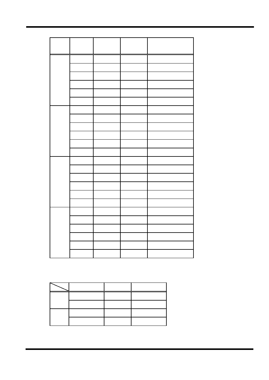
8. Instruction Set :
Instruction Code
Mnemonic
Operands
Function
Operating
Status
010000 00000000
NOP
No operation
None
010000 00000001
CLRWT
Clear Watchdog timer
0
WT
TF, PF
010000 00000010
SLEEP
Sleep mode
0
WT, stop OSC
TF, PF
010000 00000011
TMODE
Load W to TMODE register
W
TMODE
None
010000 00000100
RET
Return from subroutine
Stack
PC
None
010000 00000rrr
CPIO R
Control I/O port register
W
CPIO r
None
010001 1rrrrrrr
STWR R
Store W to register
W
R
None
011000 trrrrrrr
LDR R, t
Load register
R
t
Z
111010 iiiiiiii
LDWI I
Load immediate to W
I
W
None
010111 trrrrrrr
SWAPR R, t
Swap halves register
[R(0~3)
R(4~7)]
t
None
011001 trrrrrrr
INCR R, t
Increment register
R + 1
t
Z
011010 trrrrrrr
INCRSZ R, t
Increment register, skip if zero
R + 1
t
None
011011 trrrrrrr
ADDWR R, t
Add W and register
W + R
t
C, HC, Z
011100 trrrrrrr
SUBWR R, t
Subtract W from register
R
W
t or
(R+/W+1
t)
C, HC, Z
011101 trrrrrrr
DECR R, t
Decrement register
R
1
t
Z
011110 trrrrrrr
DECRSZ R, t
Decrement register, skip if zero
R
1
t
None
010010 trrrrrrr
ANDWR R, t
AND W and register
R
W
t
Z
110100 iiiiiiii
ANDWI i
AND W and immediate
i
W
W
Z
010011 trrrrrrr
IORWR R, t
Inclu. OR W and register
R
W
t
Z
110101 iiiiiiii
IORWI i
Inclu. OR W and immediate
i
W
W
Z
010100 trrrrrrr
XORWR R, t
Exclu. OR W and register
R
W
t
Z
110110 iiiiiiii
XORWI i
Exclu. OR W and immediate
i
W
W
Z
011111 trrrrrrr
COMR R, t
Complement register
/R
t
Z
010110 trrrrrrr
RRR R, t
Rotate right register
R(n)
R(n-1),
C
R(7), R(0)
C
C
010101 trrrrrrr
RLR R, t
Rotate left register
R(n)
r(n+1),
C
R(0), R(7)
C
C
010000 1xxxxxxx
CLRW
Clear working register
0
W
Z
010001 0rrrrrrr
CLRR R
Clear register
0
R
Z
0000bb brrrrrrr
BCR R, b
Bit clear
0
R(b)
None
0010bb brrrrrrr
BSR R, b
Bit set
1
R(b)
None
MDT10P62
This specification are subject to be changed without notice. Any latest information please preview
http;//www.mdtic.com.tw
P.14
2005/5 Ver. 1.9
Instruction Code
Mnemonic
Operands
Function
Operating
Status
0001bb brrrrrrr
BTSC R, b
Bit Test, skip if clear
Skip if R(b)=0
None
0011bb brrrrrrr
BTSS R, b
Bit Test, skip if set
Skip if R(b)=1
None
100nnn nnnnnnnn
LCALL n
Long CALL subroutine
n
PC,
PC+1
Stack
None
101nnn nnnnnnnn
LJUMP n
Long JUMP to address
n
PC
None
110111 iiiiiiii
ADDWI i
Add immediate to W
W+i
W
C,HC,Z
110001 iiiiiiii
RTWI i
Return, place immediate to W
Stack
PC,i
W
None
111000 iiiiiiii
SUBWI i
Subtract W from immediate
i-W
W
C,HC,Z
010000 00001001
RTFI
Reture from interrupt
Stack
PC,1
GIS
None
Note :
W
:
Working register
b
:
Bit position
WT
:
Watchdog timer
t
:
Target
TMODE
:
TMODE mode register
0
:
Working register
CPIO
:
Control I/O port register
1
:
General register
TF
:
Timer overflow flag
R
:
General register address
PF
:
Power loss flag
C
:
Carry flag
PC
:
Program Counter
HC :
Half carry
OSC
:
Oscillator
Z
:
Zero flag
Inclu.
:
Inclusive `
'
/
:
Complement
Exclu.
:
Exclusive `
'
x
:
Don't care
AND
:
Logic AND `
'
i
:
Immediate data ( 8 bits )
n
:
Immediate address
9. Electrical Characteristics
*Note: Temperature=25�C
1.Absolute maximum rating
Maximum current into Vdd pin : 250mA
Maximum current out of Vss pin : 300mA
Maximum current sourced by PortA : 150mA
Maximum current sourced by PortB : 200mA
Maximum current sourced by PortC : 200mA
Maximum current sunk by PortA : 150mA
Maximum current sunk by PortB : 200mA
Maximum current sunk by PortC : 200mA
Maximum output current sourced by any I/O pin : 25mA
Maximum output current sunk by any I/O pin : 25mA
These parameters are for reference only.
MDT10P62
This specification are subject to be changed without notice. Any latest information please preview
http;//www.mdtic.com.tw
P.15
2005/5 Ver. 1.9
2.Operation Current :
(1) HF (C=10p) , WDT - enable, PRD � disable
4M
10M
20M
Sleep
Sleep
WDT-disable
PRD-disable
2.5V
350u
770u
1.4m
20u
1u
3.0V
450u
880u
1.7m
37u
1u
4.0V
730u
1.4m
2.6m
42u
1u
5.0V
1.1m
2.0m
3.6m
52u
1u
5.5V
1.6m
2.9m
4.8m
80u
1u
These parameters are for reference only.
(2) XT (C=10p) , WDT - enable, PRD � disable
1M
4M
10M
Sleep
Sleep
WDT-disable
PRD-disable
2.5V
80u
220u
500u
12u
1u
3.0V
170u
400u
850u
37u
1u
4.0V
300u
700u
1.3m
42u
1u
5.0V
500u
1.0m
1.8m
52u
1u
5.5V
800u
1.4m
2.7m
80u
1u
These parameters are for reference only.
(3) LF (C=10p) , WDT - enable, PRD - disable,
32K
455K
1M
Sleep
Sleep
WDT-disable
PRD-disable
2.5V
25u (2.7V) 80u
100u
120u
1u
3.0V
35u
100u
130u
37u
1u
4.0V
50u
140u
190u
42u
1u
5.0V
100u
200u
250u
52u
1u
5.5V
200u
300u
350u
80u
1u
These parameters are for reference only.
MDT10P62
This specification are subject to be changed without notice. Any latest information please preview
http;//www.mdtic.com.tw
P.16
2005/5 Ver. 1.9
(4) RC, WDT - enable; PRD - disable; @Vdd = 5.0V
C
R
Freq.
Current
Sleep
WDT-disable
PRD-disable
4.7k
12.1M
1.9m
1u
10k
6.3M
1.1m
1u
47k
1.4M
350u
1u
100k
702K
220u
1u
300k
235K
140u
1u
3p
470k
149K
130u
1u
4.7k
5.8M
1.0m
1u
10k
2.9M
600u
1u
47k
640K
210u
1u
100k
310K
160u
1u
300k
104K
130u
1u
20p
470k
66K
120u
1u
4.7k
1.7M
380u
1u
10k
865K
250u
1u
47k
190K
140u
1u
100k
91K
130u
1u
300k
31K
110u
1u
100p
470k
19K
105u
1u
4.7k
740K
220u
1u
10k
362K
170u
1u
47k
79K
140u
1u
100k
38K
110u
1u
300k
13K
105u
1u
300p
470k
8K
105u
1u
These parameters are for reference only.
MDT10P62
This specification are subject to be changed without notice. Any latest information please preview
http;//www.mdtic.com.tw
P.17
2005/5 Ver. 1.9
RC, WDT - enable; PRD - disable; @Vdd = 3.0V
C
R
Freq.
Current
Sleep
WDT-disable
PRD-disable
4.7k
11.8M
1.1m
1u
10k
6.7M
580u
1u
47k
1.7M
190u
1u
100k
900K
150u
1u
300k
275K
80u
1u
3p
470k
176K
70u
1u
4.7k
6.4M
600u
1u
10k
3.4M
330u
1u
47k
790K
120u
1u
100k
380K
90u
1u
300k
127K
70u
1u
20p
470k
81K
60u
1u
4.7k
2.2M
230u
1u
10k
1.1M
150u
1u
47k
250K
80u
1u
100k
120K
70u
1u
300k
40K
60u
1u
100p
470k
26K
60u
1u
4.7k
1.0M
150u
1u
10k
520K
110u
1u
47k
115K
70u
1u
100k
55K
65u
1u
300k
18K
60u
1u
300p
470k
12K
60u
1u
These parameters are for reference only.
3.Input Voltage (Vdd = 5V) :
Port
Min
Max
TTL
Vss
1.0V
Vil
Schmitt trigger
Vss
0.6V
TTL
2.2V
Vdd
Vih
Schmitt trigger
3.8V
Vdd
These parameters are for reference only.
MDT10P62
This specification are subject to be changed without notice. Any latest information please preview
http;//www.mdtic.com.tw
P.18
2005/5 Ver. 1.9
Input Voltage (Vdd = 3V) :
Port
Min
Max
TTL
Vss
0.8V
Vil
Schmitt trigger
Vss
0.4V
TTL
2.0V
Vdd
Vih
Schmitt trigger
2.6V
Vdd
These parameters are for reference only.
4.Output Voltage (Vdd = 5V) :
PA,PB
Condition
Voh
4.4V
Ioh = -20mA
Vol
1.2V
Iol = 20mA
Voh
4.6V
Ioh = -5mA
Vol
0.5V
Iol = 5mA
These parameters are for reference only.
Output Voltage (Vdd = 3V) :
PA,PB
Condition
Voh
1.2V
Ioh = -20mA
Vol
0.6V
Iol = 20mA
Voh
2.4V
Ioh = -5mA
Vol
0.4V
Iol = 5mA
These parameters are for reference only.
5.The basic WDT time-out cycle time :
Time
2.5V
25
3.0V
23
4.0V
20
5.0V
17
5.5V
16
Unit = ms
These parameters are for reference only.
6.Temperature & WDT (Vdd = 5V) :
Temperature(�C)
-40
-20
0
30
50
80
WDT time(ms)
12.5
14.2
16.1
17.5
19.5
21.7
These parameters are for reference only.
MDT10P62
This specification are subject to be changed without notice. Any latest information please preview
http;//www.mdtic.com.tw
P.19
2005/5 Ver. 1.9
7.PRD :
(1)PRD reset voltage :
Voltage
Vih
4.0
�
10%
Vil
3.6
�
10%
Unit = V
These parameters are for reference only.
(2) PRD reset current :
Current
4.0V
100
3.6V
80
Unit = uA
These parameters are for reference only.
8.Pull high resistor :
Vdd
5V
3V
Pull high
45
85
Unit = K Ohm
These parameters are for reference only.
9.MCLR filter time :
Vdd=5V
Time
720
Unit = ns
These parameters are for reference only.
10.OSC1 timing requirements :
2.5us (min) LF mode (1MHz)
80ns (min) XT mode (4MHz)
External clock high or
low time (osc1)
15ns (min) HF mode (20MHz)
50ns (max) LF mode (1MHz)
15ns (max) XT mode (4MHz)
External clock rise or fall
time (osc1)
5ns (max) HF mode (20MHz)
These parameters are for reference only.
MDT10P62
This specification are subject to be changed without notice. Any latest information please preview
http;//www.mdtic.com.tw
P.20
2005/5 Ver. 1.9
11.OSC1 and CLKOUT requirements :
OSC1 high to CLKOUT high 80ns (typical) RC mode
OSC1 high to CLKOUT low
80ns (typical) RC mode
CLKOUT rise time
50ns (typical) RC mode
CLKOUT fall time
50ns (typical) RC mode
These parameters are for reference only.
12.OSC1 and PORT OUTPUT requirements :
OSC1 high to PORT OUTPUT valid
100ns (typical)
PORT OUTPUT rise time
40ns (typical)
PORT OUTPUT fall time
40ns (typical)
These parameters are for reference only.
MDT10P62
This specification are subject to be changed without notice. Any latest information please preview
http;//www.mdtic.com.tw
P.21
2005/5 Ver. 1.9
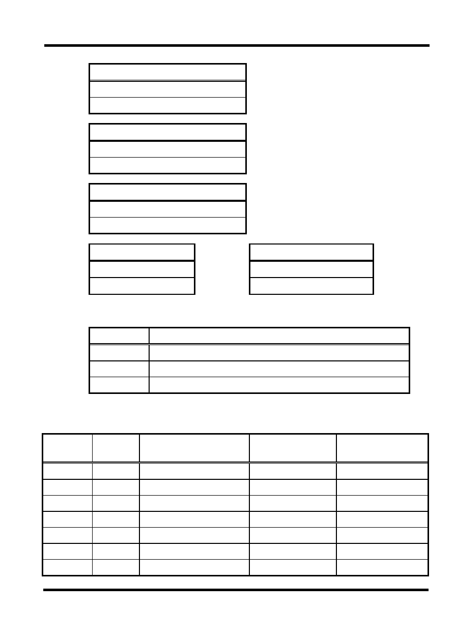
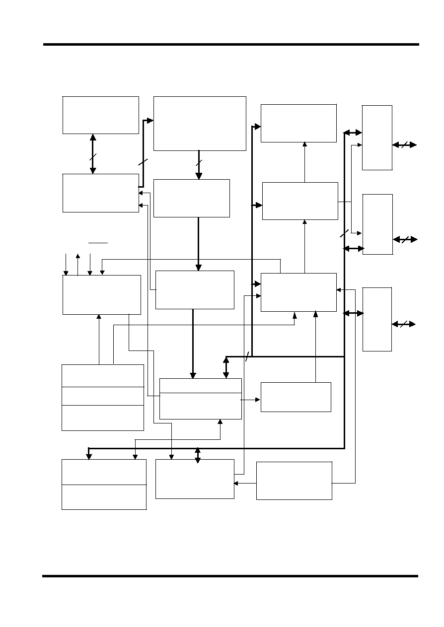
10. Block Diagram
S ta ck 8 Le ve ls
P ro g ra m C o u n te rs
O s cilla to r Circu it
P o we r o n R e s e t
P o we r Do w n Re s e t
C o u n te r / Tim e r0
E P R O M
2 Kx 1 4 (MDT1 0 P 6 2 )
In s tru ctio n
Re g is te r
In s tru ctio n
De co d e r
W o rkin g R e g is te r
ALU
S e ria l P o rt
(S CM)
RAM
1 2 8 X8
S p e c ia l Re g is te r
Co n tro l C ircu it
S ta tu s R e g is te r
W DT/O S T
Tim e r
P o rt A
P o rt B
O S C1
O S C2 MC LR
D a ta 8 -b it
1 4 b its
P ortA
P A0 ~P A5
6 b its
D0 ~ D7
P o rtC
P o rtC
P C0 ~P C 7
8 bits
P ortB
P B0 ~P B7
8 b its
Tim e r1 / Tim e r2
(C CP 1 )
P o we r R a ng e Detecto r
1 1 b its
1 1 b its