
MDT10C41A1
This specification is subject to be changed without notice. Please visit our web site for the most updated information.
http://www.mdtic.com.tw
1 of 10 Ver. 1.1
1. General Description
This 8-bit Micro-controller uses a fully static
CMOS technology to achieve high speed, small
size, low power and high noise immunity. Internal
RC oscillator
On chip memory includes 1K words of ROM, and
31 bytes of static RAM.
2. Features
u
Fully COMS static design
u
8-bit data bus
u
On chip ROM size :1 K words
u
Internal RAM size : 31 bytes
(25 general purpose registers, 6 special
registers)
u
34 single word instructions
u
14-bit instructions
u
2-level stacks
u
Operating voltage : 2.3V ~ 6 V
u
Addressing modes include direct, indirect
and relative addressing modes
u
Power-on Reset
u
RC oscillator, and R(160K) is changeable
u
12 I/O pins with their own independent
direction control
3. Applications
The application areas of this MDT10C41A1 range
from appliance motor control and high speed
automotive to low power remote
transmitters/receivers, pointing devices, and
telecommunications processors, such as Remote
controller, small instruments, chargers, toy,
automobile and PC peripheral ... etc.
4. Pin Assignment
MDT10C41A1P / MDT10C41A1S
PB4 1
16 PB3
PB5 2
15 PB2
PB6 3
14 PB1
PB7 4
13 PB0
Vdd 5
12 Vss
NC 6
11 PA3
OSCR 7
10 PA2
PA0 8
9 PA1
MDT10C41A1
This specification is subject to be changed without notice. Please visit our web site for the most updated information.
http://www.mdtic.com.tw
2 of 11 Ver. 1.1
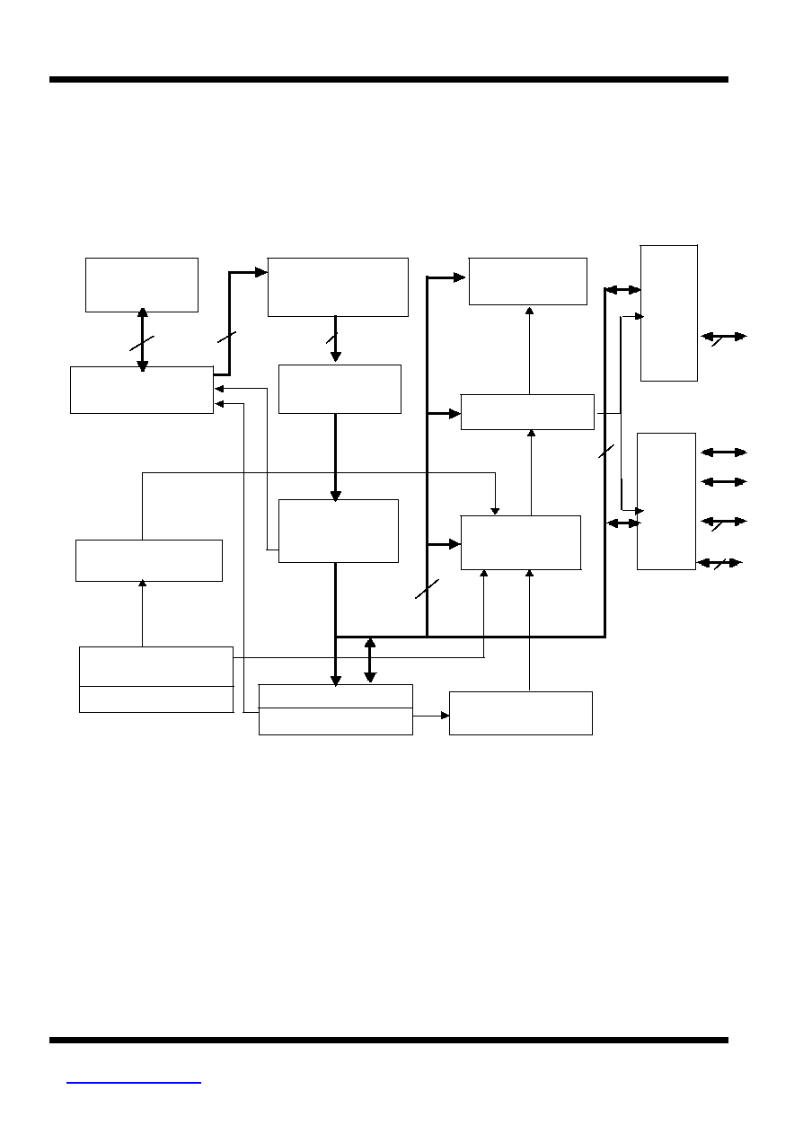
5. Block Diagram
Stack Two
Levels
Program Counters
Internal RC
Power on Reset
Power Down Reset
ROM
1024�14
Instruction
Register
Instruction
Decoder
Working Register
ALU
RAM
25�8
Special Register
Control Circuit
Status Register
Port A
Port B
Data
8bit
10 bits
10 bits
14
bits
Port
PB2 ~PB3
D0~D7
Port
PB4 ~PB7
Port
PA0~PA3
4 bits
Port PB0
Port PB1
MDT10C41A1
This specification is subject to be changed without notice. Please visit our web site for the most updated information.
http://www.mdtic.com.tw
3 of 10 Ver. 1.1
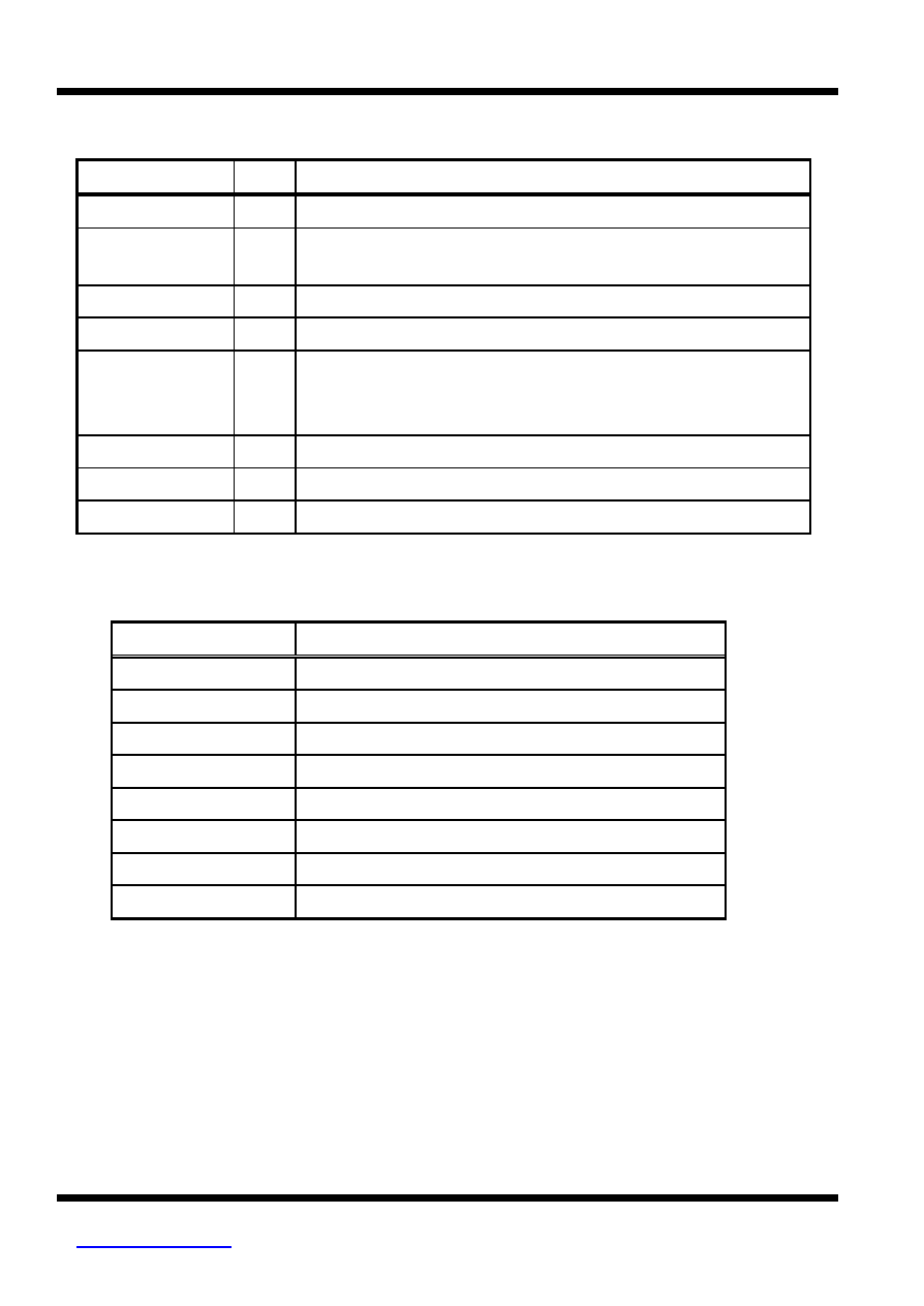
6. Pin Function Description
Pin Name
I/O
Function Description
PA0
I/O
Open drain ouput pin with 100K ohm pull-high resistor for input.
PA1~PA3
I/O
Port A, TTL input level.
PA1-PA3 are I/O pins with 50K ohm pull-high resistor for input.
PB0
I/O
I/O pin with 10K ohm pull-high resistor for input.
PB1
I/O
Open drain output with 10K ohm pull-high resistor for input.
PB2~PB3
I/O
Port B, TTL input level.
PB2-PB3 are I/O pins with weak pull-high and pull-low resistors to have
the input floating level kept about 0.7~0.8V.
PB4~PB7
I/O
Port B, TTL input level with 100K ohm pull-high resistor for input.
Vdd
Power supply
Vss
Ground
7. Memory Map
(A) Register Map
Address
Description
00
Indirect Addressing Register
01
Unimplemented
02
PC
03
STATUS
04
MSR
05
Port A
06
Port B
07~1F
Internal RAM, General Purpose Register
MDT10C41A1
This specification is subject to be changed without notice. Please visit our web site for the most updated information.
http://www.mdtic.com.tw
4 of 10 Ver. 1.1
(1) IAR ( Indirect Address Register) : R0
(2) PC (Program Counter) : R2
Write PC, CALL --- always 0
LJUMP, JUMP, LCALL --- from instruction word
RTIW, RET --- from STACK
A9
A8
A7~A0
Write PC, JUMP, CALL --- from STATUS b5
LJUMP, LCALL --- from instruction word
RTIW, RET --- from STACK
Write PC --- from ALU
LJUMP, JUMP, LCALL, CALL --- from instruction word
RTIW, RET --- from STACK
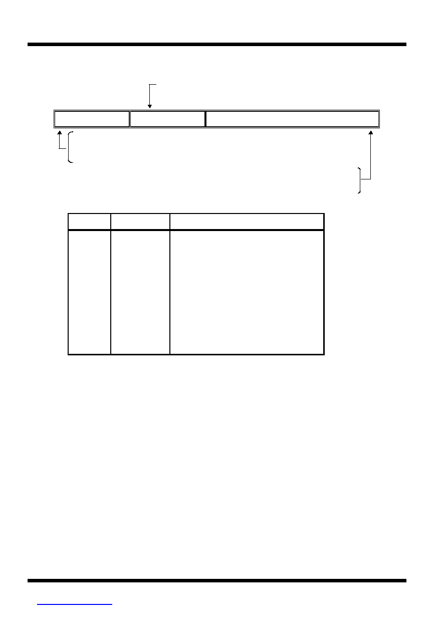
(3) STATUS (Status register) : R3
Bit
Symbol
Function
0
1
2
3
4
5
6
--
7
C
HC
Z
PF
----
page 0
----
Carry bit
Half Carry bit
Zero bit
Power loss Flag bit
Always read as high
Page select bit :
0 : 000H --- 1FFH
1 : 200H --- 3FFH
General purpose bit
(4) MSR (Memory Select Register) : R4
(5) PORT A : R5
Bit 3-0 : PA0~PA3, I/O Register
7-4 : Always read as high.
(6) PORT B : R6
PB7~PB0, I/O Register
(7) CPIO A, CPIO B (Control Port I/O Mode Register)
The CPIO register is "write-only"
"0", I/O pin in output mode;
"1", I/O pin in input mode.
MDT10C41A1
This specification is subject to be changed without notice. Please visit our web site for the most updated information.
http://www.mdtic.com.tw
5 of 10 Ver. 1.1
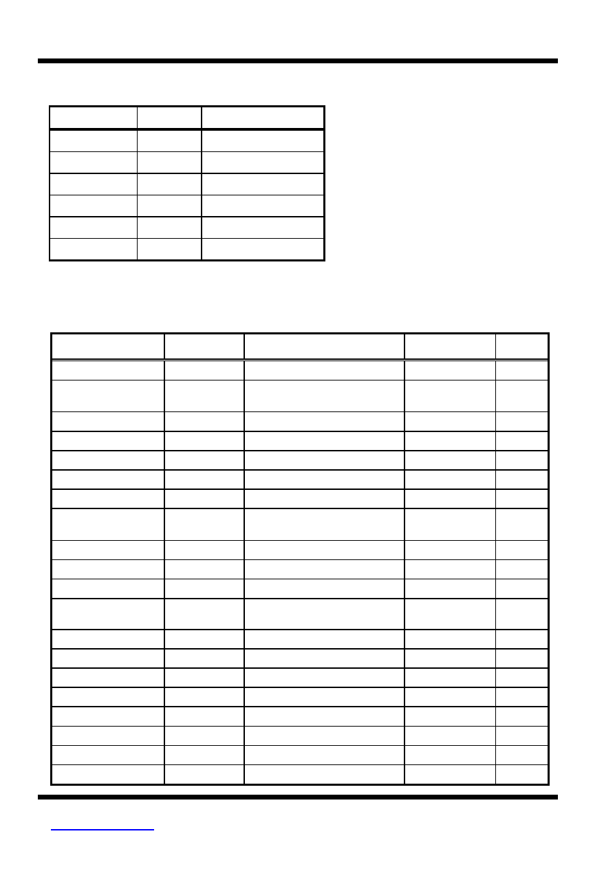
8. Reset Condition for all Registers
Register
Address
Power-On Reset
IAR
00h
PC
02h
1111 1111
STATUS
03h
0001 1xxx
MSR
04h
111x xxxx
PORT A
05h
1111 xxxx
PORT B
06h
xxxx xxxx
Note : " x "
unknown, " � "
unimplemented, read as "0"
9. Instruction Set
Instruction Code
Mnemonic
Operands
Function
Operating
Status
010000 00000000
NOP
No operation
None
010000 00000010
SLEEP
Sleep mode
0
WT,
stop OSC
TF, PF
010000 00000100
RET
Return
Stack
PC
None
010000 00000rrr
CPIO R
Control I/O port register
W
CPIO r
None
010001 1rrrrrrr
STWR R
Store W to register
W
R
None
011000 trrrrrrr
LDR R, t
Load register
R
t
Z
111010 iiiiiiii
LDWI I
Load immediate to W
I
W
None
010111 trrrrrrr
SWAPR R, t
Swap halves register
[R(0~3)
R(4~7)]
t
None
011001 trrrrrrr
INCR R, t
Increment register
R + 1
t
Z
011010 trrrrrrr
INCRSZ R, t
Increment register, skip if zero
R + 1
t
None
011011 trrrrrrr
ADDWR R, t
Add W and register
W + R
t
C, HC, Z
011100 trrrrrrr
SUBWR R, t
Subtract W from register
R
W
t
(R+/W+1
t)
C, HC, Z
011101 trrrrrrr
DECR R, t
Decrement register
R
1
t
Z
011110 trrrrrrr
DECRSZ R, t
Decrement register, skip if zero
R
1
t
None
010010 trrrrrrr
ANDWR R, t
AND W and register
R
W
t
Z
110100 iiiiiiii
ANDWI i
AND W and immediate
i
W
W
Z
010011 trrrrrrr
IORWR R, t
Inclu. OR W and register
R
W
t
Z
110101 iiiiiiii
IORWI i
Inclu. OR W and immediate
i
W
W
Z
010100 trrrrrrr
XORWR R, t
Exclu. OR W and register
R
W
t
Z
110110 iiiiiiii
XORWI i
Exclu. OR W and immediate
i
W
W
Z
MDT10C41A1
This specification is subject to be changed without notice. Please visit our web site for the most updated information.
http://www.mdtic.com.tw
6 of 10 Ver. 1.1
Instruction Code
Mnemonic
Operands
Function
Operating
Status
011111 trrrrrrr
COMR R, t
Complement register
/R
t
Z
010110 trrrrrrr
RRR R, t
Rotate right register
R(n)
R(n-1), C
R(7), R(0)
C
C
010101 trrrrrrr
RLR R, t
Rotate left register
R(n)
r(n+1),
C
R(0),
R(7)
C
C
010000 1xxxxxxx
CLRW
Clear working register
0
W
Z
010001 0rrrrrrr
CLRR R
Clear register
0
R
Z
0000bb brrrrrrr
BCR R, b
Bit clear
0
R(b)
None
0010bb brrrrrrr
BSR R, b
Bit set
1
R(b)
None
0001bb brrrrrrr
BTSC R, b
Bit Test, skip if clear
Skip if R(b)=0
None
0011bb brrrrrrr
BTSS R, b
Bit Test, skip if set
Skip if R(b)=1
None
1000nn nnnnnnnn
LCALL n
Long CALL subroutine
n
PC,
PC+1
Stack
None
1010nn nnnnnnnn
LJUMP n
Long JUMP to address
n
PC
None
110000 nnnnnnnn
CALL n
Call subroutine
n
PC,
PC+1
Stack
None
110001 iiiiiiii
RTIW i
Return, place immediate to W
Stack
PC,
i
W
None
11001n nnnnnnnn
JUMP n
JUMP to address
n
PC
None
Note :
W
: Working register b :
Bit position
CPIO
: Control I/O port register t :
Target
HC
: Half carry 0 : Working register
Z
: Zero flag
1 : General register
C
: Carry flag
PF
: Power loss flag
R
:
General register address
PC
: Program Counter
i
:
Immediate data ( 8 bits )
OSC
: Oscillator
n
:
Immediate address
Inclu.
: Inclusive `
'
/
:
Complement
Exclu.
: Exclusive `
'
x
:
Don't care
AND
: Logic AND `
'

MDT10C41A1
This specification is subject to be changed without notice. Please visit our web site for the most updated information.
http://www.mdtic.com.tw
7 of 10 Ver. 1.1
10. Electrical Characteristics
(Operating temperature at 25
).
Sym
Description
Condition
Min
Typ
Max Unit
Vdd Operating voltage
2.3
6.3
V
Fosc Internal RC oscillator frequency Vdd=5V
6.5
7
7.5 MHz
V
IL
Input Low Voltage
PA, PB
Vdd=5V
-0.6
1.0
V
V
IH
Input high Voltage
PA, PB
Vdd=5V
2.0
Vdd
V
I
IL
Input leakage current
Vdd=5V
+/-1
�
A
V
OL
Output Low Voltage
PA, PB
Vdd=5V, I
OL
=20mA
Vdd=5V, I
OL
=5mA
0.5
0.2
V
V
V
OH
Output High Voltage
PA, PB
Vdd=5V, I
OH
= -20mA
Vdd=5V, I
OH
= -5mA
4.0
4.7
V
V
V
pr
Power Edge-detector Reset
Voltage
1.2
1.5 V
MDT10C41A1
This specification is subject to be changed without notice. Please visit our web site for the most updated information.
http://www.mdtic.com.tw
8 of 10 Ver. 1.1
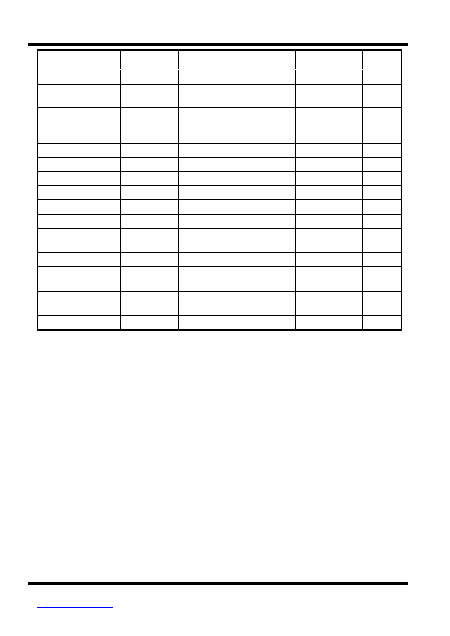
11. PA0 ~ PA3 Equivalent Circuit
I/O Control
Write
Data Bus
Read
Data O/P
Latch
D
G
D
I/O
Control
Latch
CK
Q
QB
QB
G
Q B
D
Input Resistor
Port I/O Pin
Data I/P
Latch
TTL Input Level
PA0:
Pull_Hi100K
PA1~3:
Pull_Hi 50K
(OPTION)
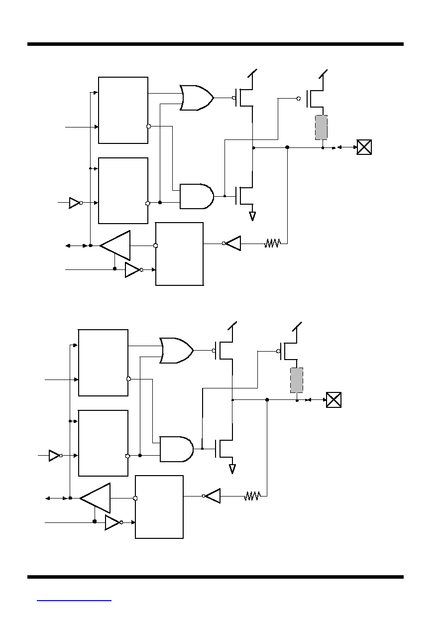
12. (A) PB0 Equivalent Circuit
I/O Control
Write
Data Bus
Read
Data O/P
Latch
D
G
D
I/O
Control
Latch
CK
Q
QB
QB
G
Q B
D
Input Resistor
Port I/O Pin
Data I/P
Latch
TTL Input Level
Pull_Hi 10K
(OPTION)
MDT10C41A1
This specification is subject to be changed without notice. Please visit our web site for the most updated information.
http://www.mdtic.com.tw
9 of 10 Ver. 1.1
I/O Control
Write
Data Bus
Read
Data O/P
Latch
D
G
D
I/O
Control
Latch
CK
Q
QB
QB
G
Q B
D
Input Resistor
Port I/O Pin
Data I/P
Latch
TTL Input Level
PULL- HIGH
100K
( OPTION )
PULL- HIGH
35 K
(OPTION)
(B) PB1 Equivalent Circuit
I/O Control
Write
Data Bus
Read
Data O/P
Latch
D
G
D
I/O
Control
Latch
CK
Q
QB
QB
G
Q B
D
Input Resistor
Port I/O Pin
Data I/P
Latch
TTL Input Level
Pull_Hi 10K
(OPTION)
(C) PB2 ~ PB3 Equivalent Circuit
MDT10C41A1
This specification is subject to be changed without notice. Please visit our web site for the most updated information.
http://www.mdtic.com.tw
10 of 10 Ver. 1.1
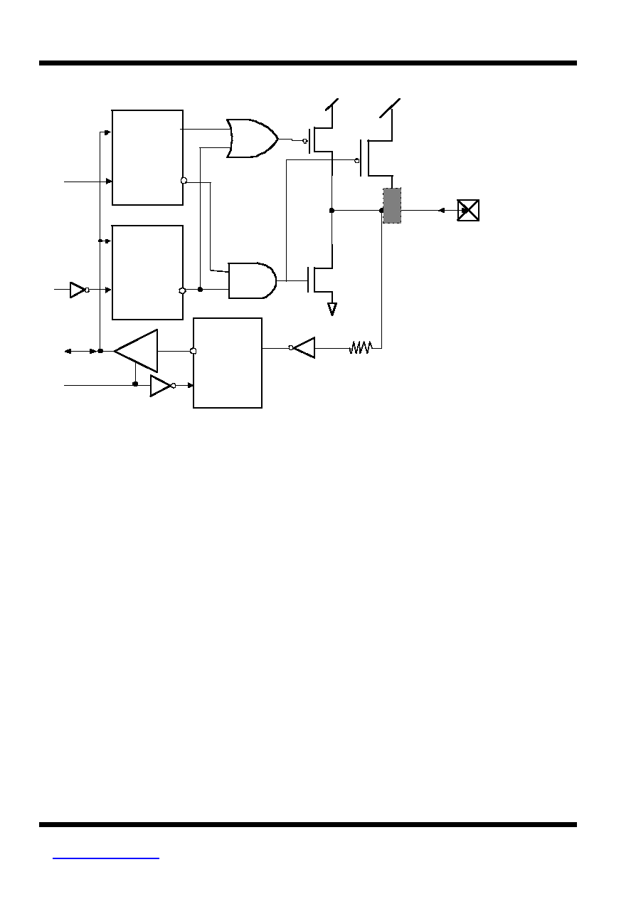
(D) PB4 ~ PB7 Equivalent Circuit
I/O Control
Write
Data Bus
Read
Data O/P
Latch
D
G
D
I/O
Control
Latch
CK
Q
QB
QB
G
Q B
D
Input Resistor
Port I/O Pin
Data I/P
Latch
TTL Input Level
Pull-Hi 100K
(OPTION)