Document Outline
- sample.pdf
- sterling.com
- Welcome to Sterling Software
- L80600.pdf

L80600
10/100/1000 Mbits/s
Ethernet PHY
R14022
TECHNICAL
MANUAL
M a r c h 2 0 0 1

ii
This document contains proprietary information of LSI Logic Corporation. The
information contained herein is not to be used by or disclosed to third parties
without the express written permission of an officer of LSI Logic Corporation.
DB14-000166-01, First Edition March 2001
This document describes the LSI Logic Corporation L80600 10/100/1000 Mbits/s
Ethernet PHY and will remain the official reference source for all
revisions/releases of this product until rescinded by an update.
To receive product literature, visit us at http://www.lsilogic.com.
LSI Logic Corporation reserves the right to make changes to any products herein
at any time without notice. LSI Logic does not assume any responsibility or
liability arising out of the application or use of any product described herein,
except as expressly agreed to in writing by LSI Logic; nor does the purchase or
use of a product from LSI Logic convey a license under any patent rights,
copyrights, trademark rights, or any other of the intellectual property rights of
LSI Logic or third parties.
Copyright � 2000, 2001 by LSI Logic Corporation. All rights reserved.
TRADEMARK ACKNOWLEDGMENT
The LSI Logic logo design is a registered trademark of LSI Logic Corporation. All
other brand and product names may be trademarks of their respective
companies.
MT

Preface
iii
Preface
This book is the primary reference and Technical Manual for the L80600
10/100/1000 Mbits/s Ethernet PHY. It contains a complete functional
description for the product and includes complete physical and electrical
specifications.
Audience
This document was prepared for logic designers and applications
engineers and is intended to provide an overview of the L80600.
This document assumes that you have some familiarity with Ethernet
LANs and related support devices. The people who benefit from this
book are:
�
Engineers and managers who are evaluating the L80600 for possible
use in a system
�
Engineers who are designing the L80600 into a system
Organization
This document has the following chapters:
�
Chapter 1, Introduction
�
Chapter 2, Functional Description
�
Chapter 3, Signals
�
Chapter 4, Registers
�
Chapter 5, Configuration Options
�
Chapter 6, Applications
�
Chapter 7, Test Conditions

iv
Preface
�
Chapter 8, Specifications
�
Chapter 9, L80600 Frequently Asked Questions
Related Publications
�
IEEE 802.3z "MAC Parameters, Physical Layer, Repeater and
Management Parameters for 1000 Mbit/s Operation."
�
IEEE 802.3ab "Physical layer specification for 1000 Mbit/s operation
on four pairs of category 5 or better balanced twisted-pair cable
(1000BASE-T)".
�
IEEE 802.3 and 802.3u (For 10/100 Mbit/s operation.)
Conventions Used in This Manual
The first time a word or phrase is defined in this manual, it is italicized.
The word assert means to drive a signal true or active. The word
deassert means to drive a signal false or inactive. Signals that are active
LOW end in an "n."
Hexadecimal numbers are indicated by the prefix "0x" --for example,
0x32CF. Binary numbers are indicated by the prefix "0b" --for example,
0b0011.0010.1100.1111.

Contents
v
Contents
Chapter 1
Introduction
1.1
General Description
1-1
1.2
Applications
1-1
1.3
Features
1-1
Chapter 2
Functional Description
2.1
Introduction
2-1
2.2
1000BASE-T Functional Description
2-3
2.2.1
1000BASE-T PCS Transmitter Block
2-4
2.2.2
1000BASE-T PMA Transmitter Block
2-7
2.2.3
1000BASE-T PMA Receiver Block
2-9
2.2.4
1000BASE-T PCS Receiver Block
2-10
2.3
Gigabit MII (GMII)
2-12
2.4
ADC/DAC/Timing Subsystem
2-14
2.5
10BASE-T and 100BASE-TX Transmitter
2-15
2.5.1
Code-Group Encoding and Injection
2-17
2.5.2
Parallel-to-Serial Converter
2-19
2.5.3
Scrambler
2-19
2.5.4
NRZ to NRZI Encoder
2-20
2.5.5
MLT-3 Converter/DAC/Line Driver
2-20
2.5.6
TX_ER
2-21
2.6
100BASE-TX Receiver
2-21
2.6.1
ADC Block
2-23
2.6.2
Signal Detect
2-23
2.6.3
BLW/EQ/AAC Correction
2-23
2.7
Clock Recovery Module
2-25
2.7.1
MLT-3 to NRZ Decoder
2-26
2.7.2
Descrambler
2-26
2.7.3
Serial to Parallel Converter
2-26

vi
Contents
2.7.4
4B/5B Decoder
2-27
2.7.5
100BASE-X Link Integrity Monitor
2-27
2.7.6
Bad SSD Detection
2-27
2.8
10BASE-T Functional Description
2-28
2.8.1
Carrier Sense
2-28
2.8.2
Collision Detect and Heartbeat
2-28
2.8.3
Link Detector/Generator
2-28
2.8.4
Jabber
2-29
2.8.5
Transmit Driver
2-29
2.9
ENDEC Module
2-29
2.9.1
Manchester Encoder and Differential Driver
2-29
2.9.2
Manchester Decoder
2-30
2.10
802.3u MII
2-30
2.10.1
Serial Management Register Access
2-30
2.10.2
Serial Management Access Protocol
2-31
2.10.3
Serial Management Preamble Suppression
2-33
2.10.4
PHY Address Sensing
2-33
2.10.5
Nibble-Wide MII Data Interface
2-33
2.10.6
Collision Detect
2-34
2.10.7
Carrier Sense
2-34
2.10.8
MII Isolate Mode
2-34
2.11
Status Information
2-35
2.11.1
Link Establishment
2-36
Chapter 3
Signals
3.1
Signal Notation
3-3
3.2
MAC Interface
3-3
3.3
Twisted-Pair (TP) Interface
3-6
3.4
JTAG Interface
3-6
3.5
EEPROM Interface
3-7
3.6
Clock Interface
3-8
3.7
LED/Interrupt Interface
3-8
3.8
Device Configuration Interface
3-10
3.9
Reset
3-13
3.10
Power And Ground Pins
3-13
3.10.1
TTL/CMOS Input/Output Supply
3-13
3.10.2
Transmit/Receive Supply
3-13

Contents
vii
3.10.3
Internal Supply Pairs
3-13
3.11
Special Connect Pins
3-14
Chapter 4
Registers
4.1
Register Notation
4-1
4.2
Standard Registers
4-2
4.2.1
Basic Mode Register (BMCR) Address 0x00
4-4
4.2.2
Basic Mode Status Register (BMSR)
Address 0x01
4-6
4.2.3
PHY Identifier Register #1 (PHYIDR1)
Address 0x02
4-9
4.2.4
PHY Identifier Resister #2 (PHYIDR2)
Address 0x03
4-10
4.2.5
AutoNegotiation Advertisement Register (ANAR)
Address 0x04
4-10
4.2.6
AutoNegotiation Link Partner Ability Register
(ANLPAR) Address 0x05
4-12
4.2.7
AutoNegotiate Expansion Register (ANER)
Address 0x06
4-14
4.2.8
AutoNegotiation Next Page Transmit Register
(ANNPTR) Address 0x07
4-15
4.2.9
AutoNegotiation Next Page Receive Register
(ANNPRR) Address 0x08
4-16
4.2.10
1000BASE-T Control Register (1KTCR)
Address 0x09
4-17
4.2.11
1000BASE-T Status Register (1KSTSR)
Address 0x0A (10)
4-19
4.2.12
Registers 0x0B�0x0E
4-20
4.2.13
1000BASE-T Extended Status Register (1KSCR)
Address 0x0F (15)
4-20
4.2.14
Strap Option Register (STRAP_REG)
Address 0x10 (16)
4-21
4.2.15
PHY Support Register (PHY_SUP)
Address 0x11 (17)
4-22
4.2.16
MDIX_SEL Address 0x15 (21)
4-23
4.2.17
EXPAND_MEM_MODE Address 0x16 (22)
4-24
4.2.18
EXP_MEM_DATA Address 0x1D (29)
4-24
4.2.19
EXP_MEM_ADDR Address 0x1E (30)
4-24

viii
Contents
4.3
Extended Registers
4-25
4.3.1
Interrupt_Status ISR0 Address 0x810D
4-26
4.3.2
Interrupt_Status ISR1 Address 0x810E
4-27
4.3.3
Interrupt_Reason IRR0 Address 0x810F
4-28
4.3.4
Interrupt_Reason IRR1 Address 0x8110
4-29
4.3.5
Interrupt_Raw_Reason RRR0 Address 0x8111
4-29
4.3.6
Interrupt_Raw_Reason RRR1 Address 0x8112
4-30
4.3.7
Interrupt_Enable IER0 Address 0x811
4-30
4.3.8
Interrupt_Enable IER1 Address 0x8114
4-31
4.3.9
Interrupt_Clear ICLR0 Address 0x8115
4-32
4.3.10
Interrupt_Clear ICLR1 Address 0x8116
4-33
4.3.11
Interrupt_Control ICTR Address 0x8117
4-34
4.3.12
AN_THRESH Address 0x8118
4-34
4.3.13
LINK_THRESH Address 0x8119
4-34
4.3.14
IEC_THRESH Address 0x811A
4-34
Chapter 5
Configuration Options
5.1
Speed/Duplex Mode Selection
5-1
5.2
Manual Mode Configurations
5-2
5.2.1
Forced Speed/Duplex Selection
5-2
5.2.2
Manual Master/Slave Resolution
5-2
5.3
AutoNegotiation
5-5
5.3.1
AutoNegotiation Priority Resolution
5-5
5.3.2
AutoNegotiation Master/Slave Resolution
5-6
5.3.3
AutoNegotiation Pause and Asymmetrical
Pause Resolution
5-6
5.3.4
AutoNegotiation Automatic MDIX Resolution
5-7
5.3.5
AutoNegotiation Strap Option Control
5-7
5.3.6
AutoNegotiation Register Control
5-8
5.3.7
AutoNegotiation Parallel Detection
5-10
5.3.8
AutoNegotiation Restart
5-11
5.3.9
Enabling AutoNegotiation through Software
5-11
5.3.10
AutoNegotiation Complete Time
5-11
5.3.11
AutoNegotiation Next Page Support
5-12
5.4
MII Isolate Mode
5-12
5.4.1
10/100 Mbits/s Isolate Mode
5-12
5.4.2
1000 Mbits/s Isolate Mode
5-12

Contents
ix
5.5
Loopback
5-13
5.6
MII/GMII Interface and Speed of Operation
5-13
5.7
Test Modes
5-14
5.8
Automatic MDI/MDIX Configuration
5-14
5.9
Polarity Correction
5-15
5.10
Firmware Interrupt
5-15
Chapter 6
Applications
6.1
Power Supply Filtering
6-1
6.2
Twisted-Pair Interface
6-3
6.3
MAC Interface
6-6
6.4
Clocks
6-7
6.5
LED/Strapping Options
6-11
6.6
Unused Pins/Reserved Pins
6-13
6.7
Hardware Reset
6-14
6.8
Temperature Considerations
6-14
6.9
System Design Implementation Consideration
6-14
6.9.1
10 Mbits/s VOD
6-15
6.9.2
Asymmetrical Pause
6-15
6.9.3
Next Page
6-16
6.9.4
LED
6-16
6.10
Pin List and Connections
6-18
Chapter 7
Test Conditions
7.1
CMOS Outputs (GMII/MII and LED)
7-2
7.2
TXD+/- Outputs (Sourcing 100BASE-TX)
7-3
7.3
TXD+/- Outputs (sourcing 1000BASE-T)
7-4
7.4
IDD Measurement Conditions
7-5
7.5
GMII Point-to-Point Test Conditions
7-5
7.6
GMII Setup and Hold Test Conditions
7-6
Chapter 8
Specifications
8.1
Absolute Maximum Ratings
8-1
8.2
Recommended Operating Conditions
8-2
8.3
Thermal Characteristics
8-2
8.4
DC Electrical Specifications
8-3
8.5
Timing
8-6

x
Contents
8.5.1
PGM Clock Timing
8-6
8.5.2
Serial Management Interface Timing
8-7
8.5.3
1000 Mbits/s Timing
8-8
8.5.4
100 Mbits/s Timing
8-10
8.5.5
AutoNegotiation Fast Link Pulse (FLP) Timing
8-14
8.5.6
Reset Timing
8-16
8.5.7
Loopback Timing
8-17
8.5.8
Isolation Timing
8-18
8.6
Packaging and Pinout
8-18
8.6.1
Pin Layout
8-18
8.6.2
PQFP Package Pin Summary
8-20
8.6.3
208-Pin Package Dimensions
8-21
Chapter 9
L80600 Frequently Asked Questions
Customer Feedback
Figures
1.1
System Diagram
1-2
2.1
L80600 Block Diagram
2-2
2.2
1000BASE-T Functional Block Diagram
2-3
2.3
PCS TX Functional Block Diagram
2-4
2.4
PMA Transmitter Block
2-7
2.5
Effect on Spectrum of PR-Shaped PAM-5 Coding
2-8
2.6
100BASE-TX Transmit Block Diagram
2-16
2.7
NRZI to MLT-3 Conversion
2-20
2.8
100BASE-TX Receive Block Diagram
2-22
2.9
100BASE-TX BLW Event
2-24
2.10
EIA/TIA Attenuation vs. Frequency for 0, 50, 100,
130 and 150 Meters of CAT-5 Cable
2-25
2.11
Typical MDC/MDIO Read Operation
2-32
2.12
Typical MDC/MDIO Write Operation
2-32
3.1
L80600 System Interfaces
3-2
6.1
Power Supply Filtering
6-2
6.2
Twisted-Pair/Magnetics Interface (Channel A Only)
6-4
6.3
125 MHz Oscillator Option
6-8
6.4
25 MHz Oscillator Option
6-9

Contents
xi
6.5
PHYAD Strapping and LED Loading Example
6-12
6.6
LED Jumper Options
6-13
7.1
CMOS Output Test Load
7-2
7.2
100 Mbits/s Twisted-Pair Load (Zero Meters)
7-3
7.3
1000 Mbits/s Twisted-Pair Load (Zero Meters)
7-4
7.4
GMII Receiver Input Potential Template
7-5
7.5
GMII Point-to-Point Test Circuit
7-5
7.6
GMII Setup and Hold Time Test Circuit
7-6
8.1
PGM Clock Timing Diagram
8-6
8.2
Serial Management Interface Timing Diagram
8-7
8.3
GMII Transmit Interface Timing Diagram
8-8
8.4
GMII Receive Timing Diagram
8-9
8.5
100 Mbits/s MII Transmit Timing Diagram
8-10
8.6
100 Mbits/s MII Receive Timing Diagram
8-10
8.7
100BASE-TX Transmit Packet Deassertion
Timing Diagram
8-11
8.8
100BASE-TX Transmit Timing Diagram (tR/F & Jitter)
8-12
8.9
100BASE-TX Receive Packet Latency Timing Diagram
8-13
8.10
100BASE-TX Receive Packet Deassertion
Timing Diagram
8-13
8.11
AutoNegotiation Fast Link Pulse (FLP) Timing Diagram
8-14
8.12
100BASE-TX Signal Detect Timing Diagram
8-15
8.13
Reset Timing Diagram
8-16
8.14
Loopback Timing Diagram
8-17
8.15
Isolation Timing Diagram
8-18
8.16
PQFP (VQM) Pin Layout
8-19
8.17
Package Dimensions
8-21
Tables
2.1
GMII/MII Mapping
2-12
2.2
4B5B Code-Group Encoding/Decoding
2-18
2.3
Typical MDIO Frame Format
2-31
2.4
Status Pins
2-35
3.1
Signal Notation
3-3
4.1
Register Notation
4-1
4.2
L80600 Standard Register Map
4-2
4.3
Extended Register Map
4-25
5.1
Non-AutoNegotiation Modes
5-2

xii
Contents
5.2
Master/Slave Rankings and Settings
5-3
5.3
Master/Slave Outcome
5-4
5.4
AutoNegotiation Modes AN_EN = 1
5-8
5.5
AutoNegotiation Disabled
5-13
5.6
AutoNegotiation Enabled
5-13
5.7
Test Mode Select
5-14
6.1
Magnetic Manufacturers
6-4
6.2
Typical Magnetics Characteristics
6-5
6.3
25 MHz Oscillator Requirements
6-9
6.4
125 MHz Oscillator Requirements
6-10
6.5
Oscillator Manufacturers
6-10
6.6
PHY Address Mapping
6-11
6.7
PHY Addresses
6-17
6.8
Pin List
6-18
8.1
Absolute Maximum Ratings
8-1
8.2
Recommended Operating Conditions
8-2
8.3
Thermal Characteristics
8-2
8.4
DC Electrical Specifications
8-3
8.5
PGM Clock Timing
8-6
8.6
Serial Management Interface Timing
8-7
8.7
GMII Transmit Interface Timing
8-8
8.8
GMII Receive Timing
8-9
8.9
100 Mbits/s MII Transmit Timing
8-10
8.10
100 Mbits/s MII Receive Timing
8-10
8.11
100BASE-TX Transmit Packet Deassertion Timing
8-11
8.12
100BASE-TX Transmit Timing
8-12
8.13
100BASE-TX Receive Packet Latency Timing
8-13
8.14
100BASE-TX Receive Packet Deassertion Timing
8-13
8.15
AutoNegotiation Fast Link Pulse (FLP) Timing
8-14
8.16
100BASE-TX Signal Detect Timing
8-15
8.17
Reset Timing
8-16
8.18
Loopback Timing
,
8-17
8.19
Isolation Timing
8-18
8.20
PQFP Package Pin Assignments
8-20
9.1
MDIX Configuration
9-9

L80600 10/100/1000 Mbits/s Ethernet PHY
1-1
Chapter 1
Introduction
1.1 General Description
The L80600 is a full-featured Physical Layer (PHY) transceiver with
integrated Physical Media Dependent (PMD) sublayers to support
10BASE-T, 100BASE-TX and 1000BASE-T Ethernet protocols.
The L80600 is designed for easy implementation of 10/100/1000 Mbits/s
Ethernet LANs. It interfaces directly to twisted-pair media by means of
an external transformer. This device interfaces directly to the Media
Access Control (MAC) layer through the IEEE 802.3u Standard Media
Independent Interface (MII) or the IEEE 802.3z Gigabit Media
Independent Interface (GMII).
1.2 Applications
The L80600 fits applications in:
�
10/100/1000 Mbits/s capable node cards
�
Switches with 10/100/1000 Mbits/s capable ports
�
High speed uplink ports (backbone)
1.3 Features
�
100BASE-TX and 1000BASE-T compliant
�
Fully compliant to IEEE 802.3u 100BASE-TX and IEEE 802.3z/ab
1000BASE-T specifications. Fully integrated and fully compliant
ANSI X3.T12 PMD physical sublayer that includes adaptive
equalization and Baseline Wander compensation.
�
10BASE-T compatible

1-2
Introduction
�
IEEE 802.3u AutoNegotiation and Parallel Detection
�
Fully AutoNegotiates between 1000 Mbits/s, 100 Mbits/s, and
10 Mbits/s full-duplex and half-duplex devices
�
Interoperates with first generation 1000BASE-T Physical layer
transceivers
�
3.3 V MAC interfaces:
IEEE 802.3u MII
IEEE 802.3z GMII
�
LED support: Link, Speed, Activity, Collision, TX and RX
�
Supports 125-MHz or 25-MHz reference clock
�
Requires only one 1.8 V and one 3.3 V supply
�
Supports MDIX at 10, 100, and 1000 Mbits/s
�
Supports JTAG (IEEE1149.1)
�
Dissipates 1 watt in 10/100 Mbits/s mode
�
Programmable Interrupts
�
208-pin PQFP package
Figure 1.1
System Diagram
Ethernet
L80600
Status
LEDs
Magnetics
RJ-45
100BASE-TX
MII/GMII
MAC
25 MHz Clock
125 MHz or
1000BASE-T
E1110
10BASE-T
10/100/1000 Mbits/s
10/100/1000 Mbits/s
Ethernet Physical Layer

L80600 10/100/1000 Mbits/s Ethernet PHY
2-1
Chapter 2
Functional Description
This chapter describes the functional blocks and operation of the
L80600. The chapter contains the following sections:
�
Section 2.1, "Introduction"
�
Section 2.2, "1000BASE-T Functional Description"
�
Section 2.3, "Gigabit MII (GMII)"
�
Section 2.4, "ADC/DAC/Timing Subsystem"
�
Section 2.5, "10BASE-T and 100BASE-TX Transmitter"
�
Section 2.6, "100BASE-TX Receiver"
�
Section 2.7, "Clock Recovery Module"
�
Section 2.8, "10BASE-T Functional Description"
�
Section 2.9, "ENDEC Module"
�
Section 2.10, "802.3u MII"
�
Section 2.11, "Status Information"
2.1 Introduction
The L80600 is a full featured 10/100/1000 Mbits/s Ethernet Physical
Layer (PHY) device, consisting of digital 10/100/1000 Mbits/s core
integrated into a single chip with a common twisted-pair interface,
combined MII/GMII controller interface, and management interface (see
Figure 2.1
).

2-2
Functional Description
Figure 2.1
L80600 Block Diagram
100BASE-TX
PCS
100BASE-TX
PMA
100BASE-TX
PMD
1000BASE-T
PCS
1000BASE-T
PMA
DAC/ADC
Subsystem
Drivers/
Receivers
Magnetics
MLT-3
100 Mbits/s
PAM-5
PR Shaped
125 Msymbols/s
4-Pair CAT-5 Cable
MII
Combined GMII, MII Interface
1000BASE-T
mC MGMT
& PHY Control
Timing
GTX_CLK
TX_EN
TXD[7:0]
TX_CLK
RX_CLK
COL
CRS
RX_ER
RX_D
V
RXD[7:0]
DAC/ADC
Timing
100BASE-TX
GMII
MII
MUX/DMUX
Management Interface
TX_ER
10BASE-T
10BASE-T
PLS
10BASE-T
PMA
Manchester
10 Mbits/s
MII
MDIO
MDC
L80600

1000BASE-T Functional Description
2-3
2.2 1000BASE-T Functional Description
The 1000BASE-T transceiver, shown in Figure 2.2, consists of a PCS
Transmitter, Physical Medium Attachment (PMA) Transmitter, PMA
Receiver, and a Physical Coding Sublayer (PCS) Receiver.
Figure 2.2
1000BASE-T Functional Block Diagram
1000BASE-T
PCS
1000BASE-T
PMA
Drivers/
Receivers
Magnetics
4-Pair CAT-5 Cable
GMII
MII
MUX/DMUX
DAC
Subsystem
PAM-5
17 Level PR Shaped
Combined GMII, MII Interface
Encode
AN
BN
CN
DN
MII (10/100 Mbits/s)
TX
AN, BN, CN, DN
PCS Receiver Functions
Delay Skew Compensation
Delay Skew Control
Forward Error Correction
Descrambler Subsystem
PMA Receiver Functions
Adaptive Equalization
Echo and Crosstalk Cancellation
Automatic Gain Control
Baseline Wander Correction
Slicer
PCS and PMA RX
1000BASE-T Block

2-4
Functional Description
2.2.1 1000BASE-T PCS Transmitter Block
The PCS transmitter consists of several functional blocks that convert the
8-bit TXD
n
data from the GMII to PAM-5 symbols to be passed onto the
PMA function. The block diagram of the PCS transmitter data path
functions in
Figure 2.3
provides an overview of each of the functional
blocks within the PCS transmitter.
Figure 2.3
PCS TX Functional Block Diagram
The transmitter consists of eight functional blocks:
�
LFSR (Linear Feedback Shift Register)
�
Data Scrambler and Symbol Sign Scrambler Word Generator
�
Scrambler Bit Generator
�
Data Scrambler
�
Convolutional Encoder
�
Bit-to-Symbol Quinary Symbol Mapping
�
Sign Scrambler Nibble Generator
�
Symbol Sign Scrambler
The requirements for the PCS transmit functionality are also defined in
the IEEE 802.3ab specification section 40.3.1.3 "PCS Transmit Function".
LSFR
g
M
= 1 + x
13
+ x
33
g
S
= 1 + x
20
+ x
33
Data Scrambler
& Symbol
Sign Scrambler
Word Generator
g(x) = x
3
x
8
Scr
n
[32:0]
Sy
n
[3:0]
Sx
n
[3:0]
Scrambler
Bit
Generator
Data
Scrambler &
Convolutional
Encoder
Bit-to
Quinary
Mapping
Sign
Scrambler
Nibble
Generator
Symbol
Sign
Scrambler
Sc
n
[7:0]
Sd
n
[8:0]
Sg
n
[3:0]
TA
n
TB
n
TC
n
TD
n
A
n
B
n
C
n
D
n
TxD
n
[7:0]
Input Data
Byte from GMII
S
n
A
n
S
n
B
n
S
n
C
n
S
n
D
n
Sign
Scrambled
PAM-5
Symbols to PMA
Symbol

1000BASE-T Functional Description
2-5
2.2.1.1 Linear Feedback Shift Register (LFSR)
The side-stream scrambler function uses a LFSR implementing one of
two equations, based on the mode of operation (master or slave). For
master operation, the equation is as follows:
g
M
(x) = 1 + x
13
+ x
33
For slave operation, use the following equation:
g
S
(x) = 1 + x
20
+ x
33
The 33-bit data output, SCR
n
[32:0], of this block is then fed into the data
scrambler and symbol sign scrambler word generator.
2.2.1.2 Data and Symbol Sign Scrambler Word Generator
The word generator uses the SCR
n
[32:0] to generate further scrambled
values. The following signals are generated: SX
n
[3:0], Sy
n
[3:0], and
Sg
n
[3:0].
The 4-bit SX
n
[3:0] and Sy
n
[3:0] values are then fed into the scrambler bit
generator. The 4-bit Sg
n
[3:0] sign values are fed into the sign scrambler
nibble generator.
2.2.1.3 Scrambler Bit Generator
This function uses the SX
n
and Sy
n
signals along with the TX_MODE
and TX_ENABLE signals to generate the SC
n
[7:0], which is further
scrambled based on the condition of the TX_MODE and TX_ENABLE
signal. The TX_MODE signal can indicate the sending of idles (SEND_I),
zeros (SEND_Z) or idles and data (SEND_N). The TX_MODE signal is
generated by the microcontroller function. The TX_ENABLE signal is
either asserted to indicate data transmission is occurring or not asserted
for no data transmission. The PCS Data Transmission Enable state
machine generates the TX_ENABLE signal.
The 8-bit SC
n
[7:0] signals are then fed into the data scrambler functional
block.

2-6
Functional Description
2.2.1.4 Data Scrambler
This function generates scrambled data by accepting the TxD
n
[7:0] data
from the GMII and scrambling it based on various inputs.
The data scrambler generates the 8-bit SD
n
[7:0] value, which scrambles
the TXD
n
data based primarily on the SC
n
values and the accompanying
control signals.
All 8-bits of SD
n
[7:0] are passed into the bit-to-quinary symbol mapping
block, while 2 bits, SD
n
[7:6], are fed into the convolutional encoder.
2.2.1.5 Convolutional Encoder
The encoder uses SD
n
[7:6] bits and TX_ENABLE to generate an
additional data bit, which is called SD
n
[8].
The one clock delayed versions CS
n
-
1
[1:0] are passed into the data
scrambler functional block. This SD
n
[8] bit is then passed into the
bit-to-symbol quinary symbol mapping function.
2.2.1.6 Bit-to-Symbol Quinary Symbol Mapping
This function implements Table 40-1 and 40-2 Bit-to-Symbol Mapping for
even and odd subsets, located in the IEEE 802.3ab specification. It takes
the 9-bit SD
n
[8:0] data and converts it to the appropriate quinary symbols
as defined by the tables.
The output of this functional block generates the TA
n
, TB
n
, TC
n
, and TD
n
symbols, which are then passed into the symbol sign scrambler.
Before describing the symbol sign scrambler, the sign scrambler nibble
generator is described, since this also feeds the symbol sign scrambler.
2.2.1.7 Sign Scrambler Nibble Generator
This function performs some further scrambling of the sign values,
Sg
n
[3:0], generated by the data scrambler and symbol sign scrambler
word generator. This sign scrambling is dependent on the TX_ENABLE
signal.
The S
n
A
n
, S
n
B
n
, S
n
C
n
, and S
n
D
n
outputs are then fed into the symbol
sign scrambler function.

1000BASE-T Functional Description
2-7
2.2.1.8 Symbol Sign Scrambler
This function scrambles the sign of the TA
n
, TB
n
, TC
n
, and TD
n
input
values from the bit-to-symbol quinary symbol mapping function, by either
inverting or not inverting the signs. This is done as follows:
A
n
= TA
n
x S
n
A
n
B
n
= TB
n
x S
n
B
n
C
n
= TC
n
x S
n
C
n
D
n
= TD
n
x S
n
D
n
The outputs of this functional block (A
n
, B
n
, C
n
, and D
n
) are the sign
scrambled PAM-5 symbols. They are then passed onto the PMA for
further processing.
2.2.2 1000BASE-T PMA Transmitter Block
The PMA transmit block shown in
Figure 2.4
contains the following
blocks:
�
Partial Response Encoder
�
100/1000 DAC Line Driver
Figure 2.4
PMA Transmitter Block
0.75
0.25
Z
-1
Table
Lookup
17-Level
PAM-5
5-Bits/
DAC
Control
20-Bits/
100/1000
MLT-3/PAM-17
Analog
Partial Response Pulse Shape Coding
5-Level PAM-5 TO 17-Level PAM
0.75*X(k) + 0.25*X(k-1)
Sign
Scrambler
PAM-5
3-Bits/
DAC
2-Bit MLT-3
PMA Transmitter Block
Sample
Sample
Sample

2-8
Functional Description
2.2.2.1 Partial Response Encoder
Partial Response (PR) coding (shaping) is used on the PAM-5 coded
signals to spectrally shape the transmitted PAM-5 signal in order to
reduce emissions in the critical frequency band ranging from 30 MHz to
60 MHz. The PR Z-transform implemented is:
The result of the PR coding on the PAM-5 signal results in 17-level
PAM-5 or PAM-17 signal that is used to drive a common 100/1000 DAC
and line driver. Without the PR coding, each signal can have five levels,
given by 1, 0.5 and 0 V. If all combinations of the five levels are used
for the present and previous outputs, then a simple table shows that
there are 17 unique output levels when PR coding is used.
Figure 2.4
shows the PMA Transmitter and the embedded PR encoder
block with its inputs and outputs.
Figure 2.5
shows the effect on the
spectrum of PAM-5 after PR shaping.
Figure 2.5
Effect on Spectrum of PR-Shaped PAM-5 Coding
2.2.2.2 10/100/1000 DAC Line Driver
The PAM-17 information from the PR encoder is used to drive a common
10/100/1000 DAC and line driver that converts digital data to suitable
analog line voltages.
0.75
0.25 Z
1
�
+
1.2
1.0
0.8
0.6
0.4
0.2
0.0
-
0.2
-
0.4
Relativ
e Amplitude
10
100
PAM-5
PAM-5
with PR (.75 + .25T)
Frequency (MHz)
Critical Region
(30 MHz�60 MHz)
Transmit Spectra

1000BASE-T Functional Description
2-9
2.2.3 1000BASE-T PMA Receiver Block
The PMA Receiver consists of several functional blocks that process the
four digitized voltage waveforms representing the received quartet of
quinary PAM-5 symbols. The DSP processing implemented in the
receiver extracts a best estimate of the quartet of quinary symbols
originated by the transmitter at the far end of the CAT-5 cable and
delivers them to the PCS RX block for further processing. There are four
separate receivers, one for each twisted-pair.
The main processing blocks include:
�
Adaptive Equalizer
�
Echo and Crosstalk Cancellers
�
Automatic Gain Control (AGC)
�
Baseline Wander (BLW) Correction
�
Slicer
2.2.3.1 Adaptive Equalizer
The Adaptive Equalizer compensates for the cable's nonideal (nonflat)
frequency versus attenuation characteristics, which results in signal
distortion. The cable attenuates the higher frequencies more than the
lower frequencies, and this attenuation difference must be equalized. The
Adaptive Equalizer is a digital filter with tap coefficients continually
adapted to minimize the Mean Square Error (MSE) value of the slicer's
error signal output. Continuous adaptation of the equalizer coefficients
means that the optimum set of coefficients are always achieved for any
given length or quality of cable.
2.2.3.2 Echo and Crosstalk Cancellers
The Echo and Crosstalk Cancellers cancel the echo and crosstalk
produced while transmitting and receiving simultaneously. Echo is
produced when the transmitted signal interferes with the received signal
on the same wire. Crosstalk is caused by the transmitted signal on each
of the other three wire pairs interfering with the receive signal of the
fourth wire pair. An Echo and Crosstalk Canceller is needed for each of
the wire pairs.

2-10
Functional Description
2.2.3.3 Automatic Gain Control (AGC)
The Automatic Gain Control acts upon the output of the Echo and
Crosstalk Cancellers to adjust the receiver gain. Different AGC methods
are available within the chip and the optimum one is selected based on
the operational state of the chip (master, slave, start-up, and so on).
2.2.3.4 Baseline Wander (BLW) Correction
BLW is the slow variation of the DC level of the incoming signal due to
the nonideal electrical characteristics of the magnetics and the inherent
DC component of the transmitted waveform. The BLW correction circuit
utilizes the slicer error signal to estimate and then correct for BLW.
2.2.3.5 Slicer
The Slicer selects the PAM-5 symbol value (+2, +1, 0,
-
1,
-
2) closest to
the voltage input value after the signal has been corrected for line
Intersymbol Interference (ISI), attenuation, echo, crosstalk and BLW.
The slicer produces an error output and symbol value decision output.
The error output is the difference between the actual voltage input and
the ideal voltage level representing the symbol value. The error output is
fed back to the BLW, AGC, Crosstalk Canceller and Echo Canceller
blocks to be used in their respective algorithms.
2.2.4 1000BASE-T PCS Receiver Block
The PCS receiver consists of several functional blocks that convert the
incoming quartet of quinary symbols (PAM-5) data from the PMA RX A,
B, C, and D to 8-bit receive data (RXD[7:0]), data valid (RX_DV), and
receive error (RX_ER) signals on the GMII. The block diagram of the
1000BASE-T Functional Block in
Figure 2.2
provides an overview of the
1000BASE-T transceiver and shows the functionality of the PCS receiver.
The major functional blocks of the PCS Receiver include:
�
Delay Skew Compensation
�
Delay Skew Control
�
Forward Error Correction (FEC)
�
Descrambler Subsystem
�
Receive State Machine

1000BASE-T Functional Description
2-11
The requirements for the PCS receive functionality are also defined in
the IEEE 802.3ab specification in section 40.3.1.4 "PCS Receive
Function."
2.2.4.1 Delay Skew Compensation
This function is used to align the received data from the four PMA
receivers and to determine the correct spatial ordering of the four
incoming twisted-pairs (which twisted-pair carries A
n
, which one carries
B
n
, and so on). The deskewed and ordered symbols are then presented
to the FEC Decoder. The differential time or time delay skew is due to
the differences in length of each of the four pairs of twisted wire in the
CAT-5 cable, manufacturing variation of the insulation of the wire pairs,
and in some cases, differences in insulation materials used in the wire
pairs. Correct symbol order to the FEC is required, since the receiver
does not have prior knowledge of the order of the incoming twisted-pairs
within the CAT-5 cable.
2.2.4.2 Delay Skew Control
This function controls the delay skew compensation function by providing
the necessary controls and selects to allow for compensation in two
dimensions (time and position). The time factor is the delay skew
between the four incoming data streams from the PMA RX A, B, C,
and D. This delay skew originates back at the input to the
ADC/DAC/Timing subsystem. Since the receiver initially does not know
the ordering of the twisted-pairs, correct ordering must be determined
automatically by the receiver during start-up. Delay skew compensation
and twisted-pair ordering is part of the training function performed during
start-up.
2.2.4.3 Forward Error Correction (FEC) Decoder
This function decodes the quartet of quinary symbols from the PMA
receivers and generates the SD
n
binary values. The FEC decoder uses
a standard 8-state Trellis code operation.
The FEC decoder decodes the quartet of quinary (PAM-5) symbols and
generates the corresponding SD
n
binary words. Initially, SD
n
[3:0] may
not have the proper bit ordering, however, correct ordering is established
by the reordering algorithm at start-up.

2-12
Functional Description
2.2.4.4 Descrambler Subsystem
The descrambler block performs the reverse scrambling function that was
implemented in the transmit section. This function works in conjunction
with the delay skew control. It provides the receiver generated SD
n
[3:0]
bits for comparison in the delay skew control function.
2.2.4.5 Receive State Machine
This state machine operation is defined in IEEE 802.3ab
section 40.3.1.4. In summary, it provides the necessary receive control
signals of RX_DV and RX_ER to the GMII. In specific conditions, as
defined in the IEEE 802.3ab specification, it generates RXD[7:0] data.
2.3 Gigabit MII (GMII)
The Gigabit Media Independent Interface (GMII) is intended for use
between Ethernet PHYs and Station Management (STA) entities and is
selected by either hardware or software configuration. The purpose of
this interface is to differentiate between the various media that are
transparent to the MAC layer.
The GMII Interface accepts either GMII or MII data, control and status
signals and routes them either to the 1000BASE-T, 100BASE-TX, or
10BASE-T modules, respectively.
The mapping between GMII and MII is illustrated in
Table 2.1
.
Table 2.1
GMII/MII Mapping
GMII
MII
RXD[3:0]
RXD[3:0]
RXD[4:7]
RX_DV
RX_DV
RX_ER
RX_ER
RX_CLK
RX_CLK
TX_CLK

Gigabit MII (GMII)
2-13
The GMII interface has the following characteristics:
�
Supports 10/100/1000 Mbit/s operation
�
Data and delimiters are synchronous to clock references
�
Provides independent 8-bit wide transmit and receive data paths
�
Provides a simple management interface
�
Uses signal levels that are compatible with common CMOS digital
ASIC processes and some bipolar processes
�
Provides for both Full-Duplex and Half-Duplex operation
The GMII interface is defined in the IEEE 802.3z document Clause 35.
In each direction of data transfer, there are data (an eight-bit bundle),
delimiter, error, and clock signals. GMII signals are defined such that an
implementation may multiplex most GMII signals with the similar PCS
service interface defined in IEEE 802.3u Clause 22.
Two media status signals are provided. One indicates the presence of
carrier (CRS), and the other indicates the occurrence of a collision
(COL). The GMII uses the MII management interface consisting of two
signals (MDC and MDIO), which provide access to management
parameters and services as specified in IEEE 802.3u Clause 22.
The MII signal names have been retained and the functions of most
signals are the same, but additional valid combinations of signals have
been defined for 1000 Mbit/s operation.
TXD[3:0]
TXD[3:0]
TXD[4:7]
TX_EN
TX_EN
TX_ER
TX_ER
GTX_CLK
COL
COL
CRS
CRS
Table 2.1
GMII/MII Mapping (Cont.)
GMII
MII

2-14
Functional Description
The Reconciliation sublayer maps the signal set provided at the GMII to
the PLS service primitives provided to the MAC.
2.4 ADC/DAC/Timing Subsystem
The 1000BASE-T receive section consists of four channels, each
receiving IEEE 802.3ab compliant PAM-5 coded data including Partial
Response (PR) shaping at 125 MBaud over a maximum of a 100 m of
CAT-5 cable. The four pairs of receive input pins are AC coupled through
the magnetics to the CAT-5 cable. Each receive pin pair is differentially
terminated with an external 100
resistor to match the cable
impedance. Each receive channel consists of a high-precision Analog to
Digital data converter (ADC) that quantizes the incoming data into a
digital word at the rate of 125 Mbits/s. The ADC is sampled with a clock
of 125 MHz recovered from the incoming data stream.
The 1000BASE-T transmit section consists of four channels, each
transmitting IEEE 802.3ab compliant 17-level PAM-5 data at
125 Msymbols/s. The four pairs of transmit output pins are AC coupled
through the magnetics to the CAT-5 cable. Each transmit pin pair is
differentially terminated with an external 100
resistor to match the
cable impedance. Each transmit channel consists of a Digital to Analog
Converter (DAC) and line driver capable of producing 17 discrete levels
corresponding to the PR shaping of a PAM-5 coded data stream. Each
DAC is clocked with a 125-MHz clock, which is the X1/Ref clock in the
Master mode of operation, and the recovered receive clock in the Slave
mode of operation.
The L80600 incorporates a sophisticated Clock Generation Module
(CGM) that supports 10/100/1000 modes of operation with an external
125 MHz clock reference (
�
50 ppm). The Clock Generation module
internally generates multiple phases of clocks at various frequencies to
support high-precision and low-jitter Clock Recovery Modules (CRM) for
robust data recovery, and to support accurate low jitter transmission of
data symbols in the Master and Slave mode of operation.

10BASE-T and 100BASE-TX Transmitter
2-15
2.5 10BASE-T and 100BASE-TX Transmitter
The 10BASE-T and 100BASE-TX transmitter consists of several
functional blocks that convert synchronous 4-bit nibble data, as provided
by the MII, to a 10 Mbit/s MLT signal for 10BASE-T operation or
scrambled MLT-3 125 Mbit/s serial data stream for 100BASE-TX
operation. Since the 10BASE-T and 100BASE-TX transmitters are
integrated with the 1000BASE-T transmitter, the differential output pins,
TD
+/-
are routed to channel A of the AC coupling magnetics.
The block diagram in
Figure 2.6
provides an overview of each functional
block within the 10BASE-T and 100BASE-TX transmit section.

2-16
Functional Description
Figure 2.6
100BASE-TX Transmit Block Diagram
The Transmitter section consists of the following functional blocks:
10BASE-T BLOCK
�
NRZ to Manchester Encoder
�
Link Pulse Generator
�
DAC/Line Driver
4B/5B Encoder
and
Injection Logic
TXDA
+/-
TX_CLK
From PGM
Parallel
to Serial
Scrambler
NRZ-to-NRZI
Binary-to-MlT
Div-by-5
100BASE-X
Loopback
NRZ to
Manchester
Encoder
Link Pulse
Generator
10/100/1000
DAC/Line Driver
TXD[3:0]/TX_ER
10BASE-T
TXD[3:0]/TX_ER
100BASE-T

10BASE-T and 100BASE-TX Transmitter
2-17
100BASE-TX BLOCK
�
4B/5B Code-Group Encoder and Injection block
�
Parallel-to-Serial block
�
Scrambler block
�
NRZ to NRZI Encoder block
�
Binary to MLT-3 Converter/DAC/Line Driver
In 10BASE-T mode, the transmitter does not meet the IEEE 802.3
specification Clause 14. This specification requires that the 10 Mbits/s
output levels are within the following limits:
VOD = 2.2 to 2.8 V peak-differential when terminated by a 100
resistor
directly at the RJ45 outputs. The L80600 10 Mbits/s output levels are
typically 1.58 V peak differential. In 10 Mbit/s operation the L80600 is
able to transmit and receive up to 187 meters of CAT-5 cable and up to
150 meters using CAT-3 cable. No impact was seen on the receive ability
of the link partner due to the reduced levels of VOD.
The L80600 implements the 100BASE-X transmit state machine diagram
as specified in the IEEE 802.3u Standard, Clause 24.
2.5.1 Code-Group Encoding and Injection
The code-group encoder converts 4-bit (4B) nibble data generated by the
MAC into 5-bit (5B) code-groups for transmission. This conversion is
required to allow control data to be combined with packet data
code-groups. Refer to
Table 2.2
for 4B to 5B code-group mapping details.
The code-group encoder substitutes the first 8-bits of the MAC preamble
with a J/K code-group pair (0b11000 0b10001) upon transmission. The
code-group encoder continues to replace subsequent 4B preamble and
data nibbles with corresponding 5B code-groups. At the end of the
transmit packet, upon the deassertion of Transmit Enable signal from the
MAC, the code-group encoder injects the T/R code-group pair
(0b01101 0b00111) indicating the end of frame.
After the T/R code-group pair, the code-group encoder continuously
injects IDLEs into the transmit data stream until the next transmit packet
is detected (reassertion of Transmit Enable).

2-18
Functional Description
Table 2.2
4B5B Code-Group Encoding/Decoding
Name
PCS 5B Code-Group
MII 4B Nibble Code
Data Codes
0
11110
0000
1
01001
0001
2
10100
0010
3
10101
0011
4
01010
0100
5
01011
0101
6
01110
0110
7
01111
0111
8
10010
1000
9
10011
1001
A
10110
1010
B
10111
1011
C
11010
1100
D
11011
1101
E
11100
1110
F
11101
1111
Idle And Control Codes
H
00100
HALT Code-Group - Error code
I
11111
Interpacket IDLE - 0000
1
J
11000
First Start of Packet - 0101
1
K
10001
Second Start of Packet - 0101
1
T
01101
First End of Packet - 0000
1
R
00111
Second End of Packet - 0000
1

10BASE-T and 100BASE-TX Transmitter
2-19
2.5.2 Parallel-to-Serial Converter
After the code-group coding and injection process, the 5-bit (5B)
code-groups are then converted to a serial data stream at 125 MHz.
2.5.3 Scrambler
The scrambler is required to control the radiated emissions at the media
connector and on the twisted-pair cable (for 100BASE-TX applications).
By scrambling the data, the total energy launched onto the cable is
randomly distributed over a wide frequency range. Without the scrambler,
energy levels at the PMD and on the cable could peak beyond FCC
limitations at frequencies related to repeating 5B sequences (continuous
transmission of IDLEs).
The scrambler is configured as a closed loop linear feedback shift
register (LFSR) with an 11-bit polynomial. The output of the closed loop
LFSR is X-OR'ed with the serial NRZ data from the serializer block. The
Invalid Codes
V
00000
0110 or 0101
2
V
00001
0110 or 0101
2
V
00010
0110 or 0101
2
V
00011
0110 or 0101
2
V
00101
0110 or 0101
2
V
00110
0110 or 0101
2
V
01000
0110 or 0101
2
V
01100
0110 or 0101
2
V
10000
0110 or 0101
2
V
11001
0110 or 0101
2
1. Control code-groups I, J, K, T and R in data fields are mapped as invalid codes,
together with RX_ER asserted.
2. Normally, invalid codes (V) are mapped to 0x6 on RXD[3:0] with RX_ER
asserted.
Table 2.2
4B5B Code-Group Encoding/Decoding (Cont.)
Name
PCS 5B Code-Group
MII 4B Nibble Code

2-20
Functional Description
result is a scrambled data stream with sufficient randomization to
decrease radiated emissions at certain frequencies by as much as
20 dB. The L80600 uses the PHY_ID (pins PHYAD [4:0]) to set a unique
seed value for the scramblers. The resulting energy generated by each
channel is out of phase with respect to each channel, thus reducing the
overall electromagnetic radiation.
2.5.4 NRZ to NRZI Encoder
After the transmit data stream has been serialized and scrambled, the
data is NRZI encoded to comply with the TP-PMD standard for
100BASE-TX transmission over Category-5 unshielded twisted-pair
cable. There is no ability to bypass this block within the L80600.
2.5.5 MLT-3 Converter/DAC/Line Driver
Binary to MLT-3 conversion is accomplished by converting the serial
NRZI data stream output from the NRZI encoder into two binary data
streams with alternately phased logic one events. These two binary
streams are then passed to a 100/1000 DAC and line driver that converts
the pulses to suitable analog line voltages. Refer to
Figure 2.7
.
Figure 2.7
NRZI to MLT-3 Conversion
The 100BASE-TX MLT-3 signal sourced by the TXDA
+/-
line driver
output pins is slew rate controlled. This should be considered when
selecting AC coupling magnetics to ensure TP-PMD Standard compliant
transition times (3 ns < t
r
< 5 ns).
NRZI_in
MLT-3_plus
NRZI_in
MLT-3_plus
MLT-3_minus
Line
Driver
MLT-3/PAM-17
differential MLT-3
MLT-3
PAM-17_in
100/1000
20
MLT-3_minus
Converter
DAC

100BASE-TX Receiver
2-21
The 100BASE-TX transmit TP-PMD function within the L80600 is
capable of sourcing only MLT-3 encoded data. Binary output from the
TXDA
+/-
outputs is not possible in 100 Mbit/s mode.
2.5.6 TX_ER
Assertion of the TX_ER input while the TX_EN input is also asserted
causes the L80600 to substitute HALT code-groups for the 5B data
present at TXD[3:0]. However, the Start-of-Stream Delimiter (SSD) /J/K/
and End-of-Stream Delimiter (ESD) /T/R/ are not substituted with HALT
code-groups. As a result, the assertion of TX_ER while TX_EN is
asserted results in a frame properly encapsulated with the /J/K/ and /T/R/
delimiters, which contain HALT code-groups in place of the data
code-groups.
2.6 100BASE-TX Receiver
The 100BASE-TX receiver consists of several functional blocks that
convert the scrambled MLT-3 125 Mbits/s serial data stream to
synchronous 4-bit nibble data that is provided to the MII. Because the
100BASE-TX TP-PMD is integrated with the 1000BASE-T, the differential
input data RXDB
+/-
is routed from channel B of the AC coupling
magnetics.
See
Figure 2.8
for a block diagram of the 100BASE-TX receive function.
This provides an overview of each functional block within the
100BASE-TX receive section.

2-22
Functional Description
Figure 2.8
100BASE-TX Receive Block Diagram
The Receive section consists of the following functional blocks:
�
ADC Block
�
Signal Detect
�
BLW/EQ/AAC Correction
�
Clock Recovery Module
4B/5B Decoder
and
Injection Logic
RXDB
+/-
RX_CLK
RXD[3:0] /
RX_ER
Serial To
Parallel
Descrambler
MLT-3
to
NRZ
BLW
EQ
AAC
Correction
ADC
Clock
Recovery
Div-by-5
SD
Signal
Detect
100BASE-TX Receive

100BASE-TX Receiver
2-23
�
MLT-3 to NRZ Decoder
�
Descrambler (bypass option)
�
Serial to Parallel
�
5B/4B Decoder (bypass option)
�
Code Group Alignment
�
4B/5B Decoder
�
Link Integrity Monitor
�
Bad SSD Detection
2.6.1 ADC Block
The L80600 requires no external attenuation circuitry at its receive
inputs, RXDB
+/-.
It accepts TP-PMD compliant waveforms directly, which
requires only a 100
termination and a simple 1:1 transformer. The
analog MLT-3 signal (with noise and system impairments) is received and
converted to the digital domain using an Analog to Digital Converter
(ADC) to allow digital signal processing (DSP) to take place on the
received signal.
2.6.2 Signal Detect
The signal detect function of the L80600 is incorporated to meet the
specifications mandated by the ANSI FDDI TP-PMD Standard as well as
the IEEE 802.3u 100BASE-TX standard for both voltage thresholds and
timing parameters.
Note:
The reception of fast link pulses per IEEE 802.3u
AutoNegotiation by the 100BASE-X receiver does not
cause the L80600 to assert signal detect.
2.6.3 BLW/EQ/AAC Correction
The digital data from the ADC block flows into the DSP Block
(BLW/EQ/AAC Correction) for processing. The DSP block applies
proprietary processing algorithms to the received signals. The algorithms
are all part of an integrated DSP receiver. The primary DSP functions
applied are:

2-24
Functional Description
�
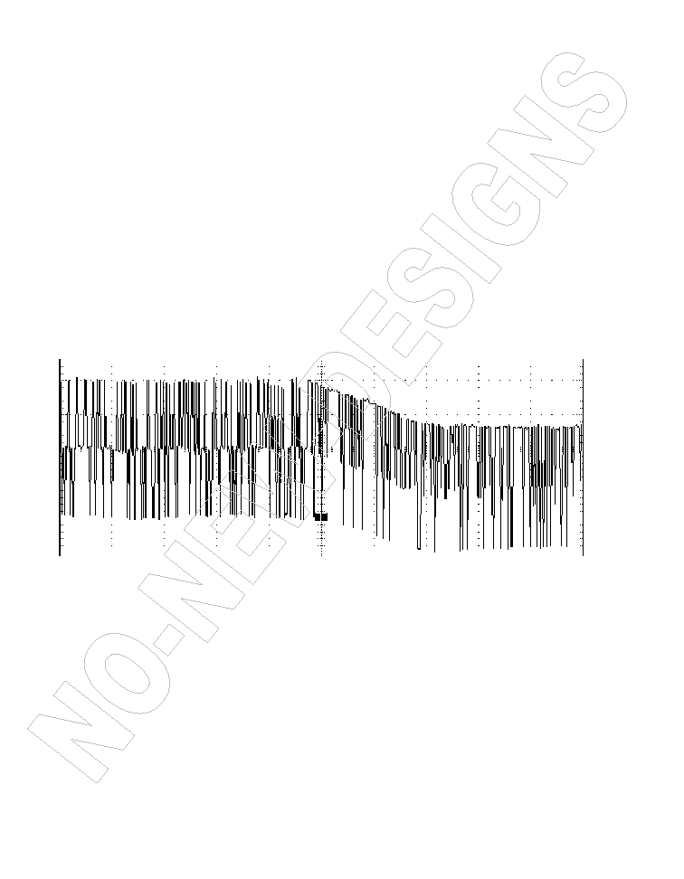
Baseline Wander (BLW). This can generally be defined as the
change in the average DC content, over time, of an AC coupled
digital transmission over a given transmission medium (copper wire).
BLW results from the interaction between the low frequency
components of a transmitted bitstream and the frequency response
of the AC coupling component(s) within the transmission system. If
the low frequency content of the digital bitstream goes below the low
frequency pole of the AC coupling transformer, the droop
characteristics of the transformer dominate, resulting in potentially
serious BLW. The digital oscilloscope plot provided in
Figure 2.9
illustrates the severity of the BLW event that can theoretically be
generated during 100BASE-TX packet transmission. This event
consists of approximately 800 mV of DC offset for a period of 120
�
s.
Left uncompensated, events such as this can cause packet loss.
Figure 2.9
100BASE-TX BLW Event
�
Signal Equalization. In high-speed twisted-pair signalling, the
frequency content of the transmitted signal can vary greatly during
normal operation based primarily on the randomness of the
scrambled data stream and is thus susceptible to frequency
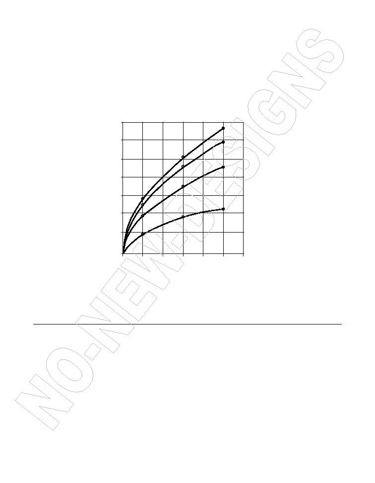
dependent attenuation (see
Figure 2.10
). This variation in signal
attenuation caused by frequency variations must be compensated for
to ensure the integrity of the transmission. To ensure quality
transmission when using MLT-3 encoding, the compensation must be
able to adapt to various cable lengths and cable types depending on
the installed environment. The selection of long cable lengths for a
given implementation requires significant compensation, which
over-compensates for shorter, less attenuating lengths. Conversely,

Clock Recovery Module
2-25
the selection of short or intermediate cable lengths requiring less
compensation causes serious under-compensation for longer length
cables. Therefore, the compensation or equalization must be
adaptive to ensure proper conditioning of the received signal,
independent of the cable length.
Figure 2.10 EIA/TIA Attenuation vs. Frequency for 0, 50, 100, 130
and 150 Meters of CAT-5 Cable
�
Automatic Attenuation Control (AAC). This allows the DSP block to
fit the resultant output signal to match the limit characteristic of its
internal decision block to ensure error free sampling.
2.7 Clock Recovery Module
The Clock Recovery Module (CRM) uses the output information from the
DSP Block to generate a phase corrected 125 MHz clock for the
100BASE-T receiver.
The CRM is implemented using an advanced digital Phase-Locked Loop
(PLL) architecture that replaces sensitive analog circuitry. Using digital
PLL circuitry allows the L80600 to be manufactured and specified to
tighter tolerances.
35
30
25
20
15
10
5
0
0
20
40
60
80
100
120
Frequency (MHz)
Atten
uation (dB)
150m
130m
100m
50m
0m

2-26
Functional Description
2.7.1 MLT-3 to NRZ Decoder
The L80600 decodes the MLT-3 information from the DSP block to binary
NRZI form and finally to NRZ data.
2.7.2 Descrambler
A serial descrambler is used to descramble the received NRZ data. The
descrambler has to generate an identical data scrambling sequence (N)
in order to recover the original unscrambled data (UD) from the
scrambled data (SD) as represented in the equations:
Synchronization of the descrambler to the original scrambling sequence
(N) is achieved based on the knowledge that the incoming scrambled
data stream consists of scrambled IDLE data. After the descrambler has
recognized 12 consecutive IDLE code-groups, where an unscrambled
IDLE code-group in 5B NRZ is equal to five consecutive ones (0b11111),
it synchronizes to the receive data stream and generates unscrambled
data in the form of unaligned 5B code-groups.
To maintain synchronization, the descrambler must continuously monitor
the validity of the unscrambled data that it generates. To ensure this, a
line state monitor and a hold timer are used to constantly monitor the
synchronization status. Upon synchronization of the descrambler, the
hold timer starts a 722
�
s countdown. Upon detection of sufficient IDLE
code-groups (16 idle symbols) within the 722
�
s period, the hold timer
resets and begins a new countdown. This monitoring operation continues
indefinitely given a properly operating network connection with good
signal integrity. If the line state monitor does not recognize sufficient
unscrambled IDLE code-groups within the 722
�
s period, the entire
descrambler is forced out of the current state of synchronization and
reset in order to reacquire synchronization.
2.7.3 Serial to Parallel Converter
The 100BASE-X receiver includes a Serial to Parallel converter. The
converter also provides code-group alignment, and operates on
unaligned serial data from the descrambler (or, if the descrambler is
bypassed, directly from the MLT-3 to NRZ decoder) and converts it into
UD
SD
N
(
)
=
SD
UD
N
(
)
=

Clock Recovery Module
2-27
5B code-group data (5 bits). Code-group alignment occurs after the J/K
code-group pair is detected. Once the J/K code-group pair
(0b11000 10001) is detected, subsequent data is aligned on a fixed
boundary.
2.7.4 4B/5B Decoder
The code-group decoder functions as a lookup table that translates
incoming 5B code-groups into 4B nibbles. The code-group decoder first
detects the J/K code-group pair preceded by IDLE code-groups and
replaces the J/K with MAC preamble. Specifically, the J/K 10-bit
code-group pair is replaced by the nibble pair (0b0101 0b0101). All
subsequent 5B code-groups are converted to the corresponding 4B
nibbles for the duration of the entire packet. This conversion ceases upon
the detection of the T/R code-group pair denoting the End of Stream
Delimiter (ESD) or with the reception of a minimum of two IDLE
code-groups.
2.7.5 100BASE-X Link Integrity Monitor
The 100BASE-X Link monitor ensures that a valid and stable link is
established before enabling both the Transmit and Receive PCS layer.
Signal Detect must be valid for at least 500
�
s to allow the link monitor
to enter the "Link Up" state, and enable transmit and receive functions.
Signal detect can be forced active by setting Bit 4 of the ECTRL1 register
0x10. Additionally, Signal Detect can be AND'ed with the descrambler
locked indication by setting Bit 3 of the EXTRL1 register. With bit 3 set,
the descrambler "Locked" is required to enter the Link Up state, but only
Signal Detect is required to maintain the link in the Link Up state.
2.7.6 Bad SSD Detection
A Bad Start of Stream Delimiter (Bad SSD) is any transition from
consecutive idle code-groups to nonidle code-groups that is not prefixed
by the code-group pair /J/K.
If this condition is detected, the L80600 asserts RX_ER and presents
RXD[3:0] = 0b1110 to the MII for the cycles that correspond to received
5B code-groups until at least two IDLE code groups are detected.

2-28
Functional Description
Once at least two IDLE code groups are detected, RX_ER and CRS
become deasserted.
2.8 10BASE-T Functional Description
This section describes the main funceions of the 10BASE-T block.
2.8.1 Carrier Sense
Carrier Sense (CRS) may be asserted due to receive activity after valid
data is detected through the Smart Squelch function.
For 10 Mbits/s Half-Duplex operation, CRS is asserted during either
packet transmission or reception.
For 10 Mbits/s Full-Duplex operation, CRS is asserted only due to
receive activity.
CRS is deasserted following an end of packet.
2.8.2 Collision Detect and Heartbeat
A collision is detected on the twisted-pair cable when the receive and
transmit channels are active simultaneously while in Half-Duplex mode.
Also after each transmission, the 10 Mbit/s block generates a Heartbeat
signal by applying a 1
�
s pulse on the COL lines that go into the MAC.
This signal is called the Signal Quality Error (SQE) and its function as
defined by IEEE 802.3 is to assure the continued functionality of the
collision circuitry.
2.8.3 Link Detector/Generator
The link generator is a timer circuit that generates a link pulse, as defined
by the 10BASE-T specification, and sent by the transmitter. The pulse,
which is 100 ns wide, is transmitted on the transmit output every 16 ms
in the absence of transmit data. The pulse is used to check the integrity
of the connection to the remote MAU.

ENDEC Module
2-29
The link detection circuit checks for valid pulses from the remote MAU. If
valid link pulses are not received, the link detector disables the
twisted-pair transmitter, receiver, and collision detection functions.
2.8.4 Jabber
The Jabber function disables the transmitter if the transmitter attempts to
transmit a longer than legal-sized packet. The jabber timer monitors the
transmitter and disables the transmission if the transmitter is active for
greater than 20�30 ms. The transmitter is then disabled for the entire
time that the ENDEC module's internal transmit is asserted. The
transmitter signal has to be deasserted for approximately 400�600 ms
(the unjab time) before the Jabber function re-enables the transmit
outputs.
There is also a jabber disable bit in the 10TOPR register (bit 5), which
when activated, disables the jabber function.
2.8.5 Transmit Driver
The 10 Mbit/s transmit driver in the L80600 uses the 100/1000 Mbits/s
common driver.
2.9 ENDEC Module
The ENDEC consists of two major blocks:
�
The Manchester Encoder. It accepts NRZ data from the controller,
Manchester encodes it, and transmits it differentially to the
transceiver through the differential transmit driver.
�
The Manchester Decoder. It receives Manchester data from the
transceiver, converts it to NRZ data, and recovers clock pulses and
sends them to the controller.
2.9.1 Manchester Encoder and Differential Driver
The Manchester encoder begins operation when the Transmit Enable
input (TX_EN) goes HIGH. The encoder then converts the clock and
NRZ data to Manchester data for the transceiver. As long as TX_EN is
HIGH, the Transmit Data (TXD) is encoded for the transmit-driver pair

2-30
Functional Description
(TX ).TXD must be valid on the rising edge of the Transmit Clock
(TX_CLK). Transmission ends when TX_EN goes LOW. The last
transition is always positive; it occurs at the center of the bit cell if the
last bit is a one, or at the end of the bit cell if the last bit is a zero.
2.9.2 Manchester Decoder
The Manchester decoder consists of a differential receiver and a PLL to
separate the Manchester encoded data stream into internal clock signals
and data. Once the input exceeds the squelch requirements, Carrier
Sense (CRS) is asserted off the first edge presented to the decoder.
Once the decoder has locked onto the incoming data stream, it provides
data (RXD) and clock (RX_CLK) to the MAC.
The decoder detects the end of a frame when no more midbit transitions
are detected. Typically, within one and a half bit times after the last bit,
carrier sense (CRS) is deasserted. Receive clock stays active for at least
five more bit times after CRS goes LOW, to guarantee the receive timing
of the controller.
2.10 802.3u MII
The L80600 incorporates the Media Independent Interface (MII) as
specified in Clause 22 of the IEEE 802.3u standard. This interface may
be used to connect PHY devices to a MAC in 10/100 Mbit/s mode. This
section describes both the serial MII management interface as well as
the nibble wide MII data interface.
The serial management interface of the MII allows for the configuration
and control of multiple PHY devices, gathering of status and error
information, and the determination of the type and capabilities of the
attached PHY(s).
The nibble wide MII data interface consists of a receive bus and a
transmit bus, each with control signals to facilitate data transfer between
the PHY and the upper layer (MAC).
2.10.1 Serial Management Register Access
The serial management MII specification defines a set of thirty-two 16-bit
status and control registers that are accessible through the management

802.3u MII
2-31
interface pins MDC and MDIO for 10/100/1000 Mbit/s operation. The
L80600 implements all the required MII registers as well as several
optional registers. These registers are fully described in
Chapter 4,
"Registers."
A description of the serial management access protocol
follows.
2.10.2 Serial Management Access Protocol
The serial control interface consists of two pins, Management Data Clock
(MDC) and Management Data Input/Output (MDIO). MDC has a
maximum clock rate of 2.5 MHz and no minimum rate. The MDIO line is
bidirectional and may be shared by up to 32 devices. The MDIO frame
format is shown below in
Table 2.3
.
The MDIO pin requires a pull-up resistor (1.5 k
) which, during IDLE and
turnaround, pulls MDIO HIGH. To initialize the MDIO interface, the station
management entity sends a sequence of 32 contiguous logic ones on
MDIO to provide the L80600 with a sequence that can be used to
establish synchronization. This preamble may be generated either by
driving MDIO HIGH for 32 consecutive MDC clock cycles, or by simply
allowing the MDIO pull-up resistor to pull the MDIO pin HIGH during
which time 32 MDC clock cycles are provided. In addition, 32 MDC clock
cycles should be used to resynchronize the device if an invalid start,
opcode, or turnaround bit is detected.
The L80600 waits until it has received this preamble sequence before
responding to any other transaction. Once the L80600 serial
management port has been initialized, no further preamble sequencing
is required until after a power-on/reset, invalid start, invalid opcode, or
invalid turnaround bit has occurred.
The Start code is indicated by an <01> pattern. This assures the MDIO
line transitions from the default idle line state.
Table 2.3
Typical MDIO Frame Format
MII Management
Serial Protocol
<idle><start><op code><device addr><reg addr><turnaround><data><idle>
Read Operation
<idle><01><10><AAAAA><RRRRR><Z0><xxxx xxxx xxxx xxxx><idle>
Write Operation
<idle><01><01><AAAAA><RRRRR><10><xxxx xxxx xxxx xxxx><idle>

2-32
Functional Description
Turnaround is defined as an idle bit time inserted between the Register
Address field and the Data field. To avoid contention during a read
transaction, no device is allowed to actively drive the MDIO signal during
the first bit of turnaround. The addressed L80600 drives the MDIO with
a zero for the second bit of turnaround and follows this with the required
data.
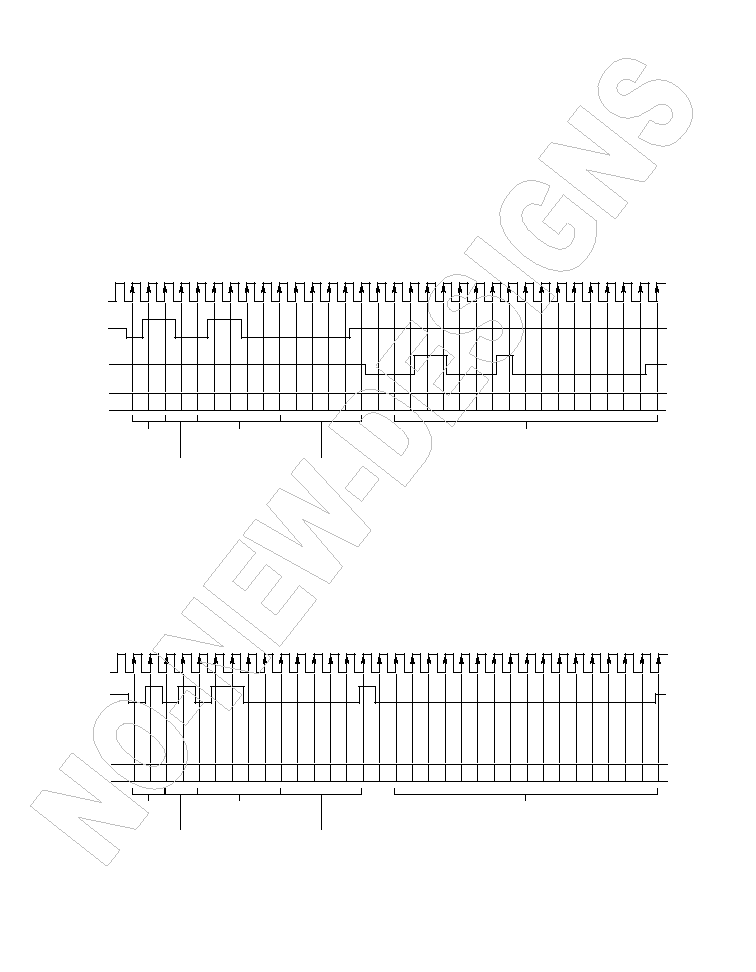
Figure 2.11
shows the timing relationship between MDC and the
MDIO as driven/received by the Station (STA) and the L80600 (PHY) for
a typical register read access.
Figure 2.11 Typical MDC/MDIO Read Operation
For write transactions, the station management entity writes data to the
addressed L80600, eliminating the requirement for MDIO Turnaround.
The turnaround time is filled by the management entity by inserting <10>.
Figure 2.12
shows the timing relationship for a typical MII register write
access.
Figure 2.12 Typical MDC/MDIO Write Operation
MDC
MDIO
0
0 0
1 1
1 1 0 0 0 0 0 0 0
(STA)
Idle
Start
PHY Address
(PHYAD = 0x0C)
Register Address
(0x00 = BMCR)
TA
Register Data
Z
MDIO
(PHY)
Z
Z
Z
0 0 0 1 1 0 0 0 1 0 0 0 0 0 0 0 0 Z
Idle
Z
Z
Opcode
(Read)
MDIO
0
0
0
1
1
1 1 0 0 0 0 0 0 0
(STA)
Z
0 0 0
0 0 0
0 0 0 0 0 0 0 0 Z
1
0 0
0
Z
Z
Idle
Start
PHY Address
(PHYAD = 0x0C)
Register Address
(0x00 = BMCR)
TA
Register Data
Idle
Opcode
(Write)

802.3u MII
2-33
2.10.3 Serial Management Preamble Suppression
The L80600 supports a Preamble Suppression mode as indicated by a
one in bit 6 of the Basic Mode Status Register (BMSR, address 0x01).
If the station management entity (MAC or other management controller)
determines that all PHYs in the system support Preamble Suppression
by returning a one in this bit, then the station management entity need
not generate preamble for each management transaction.
The L80600 requires a single initialization sequence of 32 bits of
preamble following power-up/hardware reset. This requirement is
generally met by the mandatory pull-up resistor on MDIO in conjunction
with a continuous MDC, or the management access made to determine
whether Preamble Suppression is supported.
While the L80600 requires an initial preamble sequence of 32 bits for
management initialization, it does not require a full 32-bit sequence
between each subsequent transaction. A minimum of one idle bit
between management transactions is required as specified in
IEEE 802.3u.
2.10.4 PHY Address Sensing
The L80600 provides five PHY address pins. The information from these
pins is latched into the ECTLR1 register (address 0x10, bits [10:6]) at
device power-up or reset. The L80600 supports PHY Address strapping
values 0 (<00000>) through 31 (<11111>). PHY Address 0 puts the
device into Isolate Mode.
2.10.5 Nibble-Wide MII Data Interface
Clause 22 of the IEEE 802.3u specification defines the Media
Independent Interface (MII). This interface includes a dedicated receive
bus and a dedicated transmit bus. These two data buses, along with
various control and indicate signals, allow for the simultaneous exchange
of data between the L80600 and the upper layer agent (MAC).
The receive interface consists of a nibble wide data bus RXD[3:0], a
receive error signal RX_ER, a receive data valid flag RX_DV, and a
receive clock RX_CLK for synchronous transfer of the data. The receive
clock operates at 25 MHz to support 100 Mbit/s operation.

2-34
Functional Description
The transmit interface consists of a nibble wide data bus TXD[3:0], a
transmit error flag TX_ER, a transmit enable control signal TX_EN, and
a transmit clock TX_CLK operating at 25 MHz.
Additionally, the MII includes the carrier sense signal CRS, as well as a
collision detect signal COL. The CRS signal asserts to indicate the
reception of data from the network or as a function of transmit data in
Half-Duplex mode. The COL signal asserts as an indication of a collision
that can occur during Half-Duplex operation when both a transmit and
receive operation occur simultaneously.
2.10.6 Collision Detect
For Half-Duplex, a 10/100BASE-TX collision is detected when the
receive and transmit channels are active simultaneously. Collisions are
reported by the COL signal on the MII.
2.10.7 Carrier Sense
Carrier Sense (CRS) may be asserted during 10/100 Mbit/s operation
when a valid link (SD) and two noncontiguous zeros are detected on the
line.
For 10/100 Mbit/s Half-Duplex operation, CRS is asserted during either
packet transmission or reception.
For 10/100 Mbit/s Full-Duplex operation, CRS is asserted only due to
receive activity.
CRS is deasserted following an end of packet.
2.10.8 MII Isolate Mode
The L80600 can be set to Isolate Mode by setting bit 10 in the Basic
Mode Control Register (0x00) to 1.
With bit 10 in the BMCR set to one, the L80600 does not respond to
packet data present at TXD[3:0], TX_EN, and TX_ER inputs and
presents a high impedance on the TX_CLK, RX_CLK, RX_DV, RX_ER,
RXD[3:0], COL, and CRS outputs. The L80600 continues to respond to
all serial management transactions over the MDIO/MDC lines.

Status Information
2-35
While in Isolate mode, the TXD
+/-
outputs are dependent on the current
state of AutoNegotiation. The L80600 can AutoNegotiate or parallel
detect to a specific technology depending on the receive signal at the
RXD
+/-
inputs. A valid link can be established for RXD even when the
L80600 is in Isolate mode.
The user should have a basic understanding of Clause 22 of the
IEEE 802.3u standard.
2.11 Status Information
There are 9 pins available to convey status information to the user
through LEDs. The 9 pins indicate link status, collision status, duplex
status, activity, device speed indication, and separate indications for
receive (RX) and transmit (TX) for the device. The pin functions are
shown in
Table 2.4
.
Table 2.4
Status Pins
Pin
Description
LED_LNK
Indicates Good Link Status for 100BASE-TX and
1000BASE-T.
LED_COL
Indicates that the PHY has detected a collision condition
(simultaneous transmit and receive activity while in
Half-Duplex mode).
LED_DUPLEX
Indicates that the L80600 is in Full-Duplex mode of
operation.
LED_ACT
Indicates Receive or Transmit activity.
LED_10
Indicates that the PHY is in 10BASE-T mode.
LED_100
Indicate that s the PHY is in 100BASE-TX mode.
LED_1000
Indicates that the PHY is in 1000BASE-T mode.
LED_TX
Indicates that the PHY is transmitting.
LED_RX
Indicates that the PHY is receiving.

2-36
Functional Description
2.11.1 Link Establishment
For 10BASE-T, a link is established if Normal Link Pulses are detected
that are separated by 16 ms or by packet data received.
For 100BASE-T, a link is established as a result of an input receive
amplitude compliant with TP-PMD specifications that result in internal
generation of Signal Detect. LED_LNK is asserted after the internal
Signal Detect has remained asserted for a minimum of 500
�
s.
LED_LNK is deasserted immediately following the deassertion of the
internal Signal Detect.
For 1000BASE-T, a link is established as a result of training,
AutoNegotiation completed, and reliable reception of signals transmitted
from a remote PHY.

L80600 10/100/1000 Mbits/s Ethernet PHY
3-1
Chapter 3
Signals
This chapter contains detailed descriptions of each of the L80600
signals. The chapter contains the following sections:
�
Section 3.1, "Signal Notation"
�
Section 3.2, "MAC Interface"
�
Section 3.3, "Twisted-Pair (TP) Interface"
�
Section 3.4, "JTAG Interface"
�
Section 3.5, "EEPROM Interface"
�
Section 3.6, "Clock Interface"
�
Section 3.7, "LED/Interrupt Interface"
�
Section 3.8, "Device Configuration Interface"
�
Section 3.9, "Reset"
�
Section 3.10, "Power And Ground Pins"
�
Section 3.11, "Special Connect Pins"

3-2
Signals
Figure 3.1
L80600 System Interfaces
MDC
MDIO
CRS
COL
TX_CLK
TXD[7:0]
TX_EN
GTX_CLK
TX_ER
RX_CLK
RXD[7:0]
RX_ER
RX_DV
TXDA+/-
TXDB+/-
TXDC+/-
TXDD+/-
RXDA+/-
RXDB+/-
RXDC+/-
RXDD+/-
TRSTn
TDI
TDO
TMS
TCK
SDA
SCL
REF_CLK
REF_SEL
LED_RX
LED_TX
LED_LINK
LED_DUPLEX
LED_COL
LED_ACT
LED_10
LED_100
LED_1000
INT
AN_EN/TX_TCLK
MANUAL_M/S/Enable
Manual M/S Advertise
1000FDX_ADV
LED_DUPLEX/1000HDX_ADV
100_ADV
NC MODE
SPEED[1]/10_ADV
SPEED[0]/PORT_TYPE
PHYAD_[4:0]
RESETn
MAC
Interface
TP
Interface
JTAG
Interface
E
2
PROM
Interface
Clock
Interface
LED/Interrupt
Interface
Reset
Device
Configuration
Interface
L80600

Signal Notation
3-3
3.1 Signal Notation
The notation convention for each of the signal descriptions given in this
chapter is given in
Table 3.1
.
In addition to the noations listed in
Table 3.1
, the pin number associated
with each signal is listed in each description.
3.2 MAC Interface
The following signals allow the device to communicate with a MAC.
MDC
Management Data Clock
I 151
Synchronous clock to the MDIO management data
input/output serial interface that may be asynchronous to
the transmit and receive clocks. The maximum clock rate
is 2.5 MHz. There is no minimum clock rate.
Table 3.1
Signal Notation
Notation
Meaning
I
Input
O
Output
I/O
Bidirectional
Z
3-State
O_Z
3-State Output
I/O_Z
3-State Input_Output
S
Strapping Pin
PU
Pull-Up
PD
Pull-Down
S
Strap Option (the pin may be strapped HIGH or
LOW for power-up or reset configuration
options)

3-4
Signals
MDIO
Management Data I/O
IO 150
Bidirectional management instruction/data signal that
may be sourced by the station management entity or the
PHY. This pin requires a 1.5 k
pullup resistor.
CRS
Carrier Sense
O 111
Asserted HIGH to indicate the presence of carrier due to
receive or transmit activity in Half-Duplex mode. This
signal is not defined and is LOW for 1000BASE-T
Full-Duplex mode. For 100BASE-TX Full-Duplex
operation, CRS is asserted only for receive activity.
COL
Collision Detect
O 110
Asserted HIGH to indicate detection of a collision
condition (simultaneous transmit and receive activity) in
Half-Duplex modes. This signal is not synchronous to
either MII clock (GTX_CLK, TX_CLK or RX_CLK). This
signal is not defined and is LOW for Full-Duplex mode.
TX_CLK
Transmit Clock (100 Mbits/s)
O 130
Continuous clock signal generated from REF_CLK and
driven by the PHY during 100 Mbit/s operation. It is used
on the MII to clock all MII Transmit (TXD[7:0], TX_ER),
signals into the PHY.
The Transmit Clock frequency is constant and the
frequency is 25% of the nominal MII transmit data bit rate
for parallel transfers (25 MHz) for 100BASE-TX.
TX_CLK should not be confused with the TX_TCLK
signal.
TXD[7:0]
Transmit Data
I [135, 138:141, 144:146]
These signals carry 4B data nibbles (TXD[3:0]) during
100 Mbit/s MII mode and 8-bit data (TXD[7:0]) in
1000 Mbit/s GMII mode. They are synchronous to the
Transmit Clocks (TX_CLK, GTX_CLK). TX_EN, when
asserted, enables transmit data for all modes, all sourced
by the controller.
TX_EN
Transmit Enable
I 134
Active HIGH input driven by the MAC when it requests
transmission of the data present on the TXD lines (nibble
data for 100 Mbit/s mode and 8-bit data for 1000 Mbit/s
GMII mode.)

MAC Interface
3-5
GTX_CLK
GMII Transmit Clock
I 147
This continuous clock signal is sourced from the upper
level MAC to the PHY. The nominal frequency is
125 MHz, which is derived in the MAC from its 125 MHz
reference clock. In most applications, it is the same
referenced clock the PHY uses.
TX_ER
Transmit Error
I 133
Active HIGH input during 100 Mbit/s nibble mode and
1000 Mbit/s GMII mode and forces the PHY to transmit
invalid symbols. The TX_ER signal must be synchronous
to the Transmit Clocks (TX_CLK and GTX_CLK).
In 4B nibble mode, assertion of Transmit Error by the
controller causes the PHY to issue invalid symbols
followed by HALT (H) symbols until TX_ER is deasserted.
In 1000 Mbit/s GMII mode, assertion causes the PHY to
emit one or more code-groups that are not valid data or
delimiter set in the transmitted frame.
RX_CLK
Receive Clock
O 126
Provides the recovered following receive clocks for
different modes of operation:
25 MHz nibble clock in 100 Mbit/s nibble mode.
125 MHz byte clock in 1000 Mbit/s GMII mode.
RXD[7:0]
Receive Data
O [114:115, 118:121, 124:125}
These signals carry 4-bit data nibbles (RXD[3:0]) during
100 Mbit/s MII mode and 8-bit data bytes (RXD[7:0]) in
1000 Mbit/s GMII mode. They are synchronous to the
Receive Clock (RX_CLK). Receive data is driven by the
PHY to the controller, and is strobed by Receive Data
Valid (RX_DV), which is also sourced by the PHY.
RX_ER
Receive Error
O 112
In 100 Mbit/s nibble mode and 1000 Mbit/s GMII mode,
this active-HIGH output indicates that the PHY has
detected a Receive Error. The RX_ER signal must be
synchronous with the Receive Clock (RX_CLK).
RX_DV
Receive Data Valid
O 113
Asserted HIGH to indicate that valid data is present on
the corresponding RXD[3:0] for 100 Mbit/s nibble mode
and RXD[7:0] in 1000 Mbit/s GMII mode.

3-6
Signals
3.3 Twisted-Pair (TP) Interface
The following signals provide the means for the L80600 to communicate
to the media.
TXD[A:D]+/-
Transmit Data
O [9:10, 13:14, 39:40, 43:44]
The TP Interface connects the L80600 to the CAT-5 cable
through a single common magnetics transformer. The
Transmit (TXD) and Receive (RXD) twisted-pair pins
carry bit-serial data at a 125 MHz baud rate. These
differential outputs are configurable to either
100BASE-TX or 1000BASE-T signalling as follows:
100BASE-TX: Transmission of 3-level MLT-3 data.
1000BASE-T: Transmission of 17-level PAM-5 with
PR-shaping data.
The L80600 automatically configures the common driver
outputs for the proper signal type as a result of either
forced configuration or AutoNegotiation.
Note:
During 10/100 Mbit/s operation, only TXDA+ and TXDA-
are active
RXD[A:D]+/-
Receive Data
I[4:5, 18:19, 34:35, 48:49]
Differential receive signals.
Note:
During 10/100 Mbit/s operation, only RXDB+ and RXDB-
are active.
3.4 JTAG Interface
This section describes the JTAG signals used for device testing.
TRSTn
Test Reset
I 156
IEEE 1149.1 Test Reset pin. This pin is an active-LOW
reset and provides for asynchronous reset of the Tap
Controller. This reset has no effect on the device
registers.
This pin should be tied LOW during regular chip
operation.

EEPROM Interface
3-7
TDI
Test Data Input
I 157
IEEE 1149.1 Test Data Input pin. This pin is the test data
scanned into the device through TDI.
This pin should be tied LOW during regular chip
operation.
TDO
Test Data Output
O 158
IEEE 1149.1 Test Data Output pin. The most recent test
results are scanned out of the device through TDO.
This pin can be left floating if not used.
TMS
Test Mode Select
I 159
IEEE 1149.1 Test Mode Select pin. This pin sequences
the Tap Controller (16-state FSM) to select the desired
test instruction.
This pin should be tied LOW during regular chip
operation.
TCK
Test Clock
I 163
IEEE 1149.1 Test Clock input. This pin is the primary
clock source for all test logic input and output controlled
by the testing entity.
This pin should be tied LOW during regular chip
operation.
3.5 EEPROM Interface
The EEPROM signals are given in this section.
SDA
Serial Data
I/O PU 189
This pin is used for EEPROM data. It should be left
floating if the EEPROM interface is not used.
SCL
Serial Clock
I/O PD 190
This pin is used for EEPROM clock. It should be left
floating if the EEPROM interface is not used.

3-8
Signals
3.6 Clock Interface
This section describes the clock and clock select signals.
REF_CLK
Clock Input
I 153
125 MHz or 25 MHz (both require
�
50 ppm tolerance and
less than 200 ps of jitter).
REF_SEL
Clock Select
I 154
This pin enables the use of a 125 MHz clock source to
REF_CLK when left floating and enables a 25 MHz clock
source when pulled LOW.
3.7 LED/Interrupt Interface
This section describes the LED and interrupt signals. See
Section 6.5,
"LED/Strapping Options"
for more information regarding how to use these
signals and their active states.
LED_RX
Receive Activity LED
I/O, S, PD 207
The Receive LED output indicates that the PHY is
receiving.
LED_TX
Transmit Activity LED
I/O, S, PD 205
The Transmit LED output indicates that the PHY is
transmitting.
LED_LNK
Good Link LED Status
I/O, S, PD 204
Indicates status for Good Link. The criteria for good link
are:
10BASE-T: Link is established by detecting Normal Link
Pulses separated by 16 ms or by packet data received.
100BASE-T: Link is established as a result of an input
receive amplitude compliant with TP-PMD specifications
that results in internal generation of Signal Detect.
LED_LNK is asserted after the internal Signal Detect has
remained asserted for a minimum of 500
�
s. LED_LNK
is deasserted immediately following the deassertion of
the internal Signal Detect.

LED/Interrupt Interface
3-9
1000BASE-T: Link is established as a result of training,
AutoNegotiation completed, valid 1000BASE-T link
established and reliable reception of signals transmitted
from a remote PHY is established.
LED_DUPLEX
Duplex LED Status
I/O, S, PD 185
If LED_DUPLEX is asserted, it indicates the Full-Duplex
mode of operation is active. If it is deasserted, it indicates
that the device is in Half-Duplex mode.
LED_COL
Collision LED Status
I/O, S, PD 201
Indicates that the PHY has detected a collision condition
(simultaneous transmit and receive activity while in
Half-Duplex mode).
LED_ACT
TX/RX Activity LED Status
I/O, S, PU 200
Indicates either transmit or receive activity.
LED_10
10 Mbit/s Speed LED
I/O, S, PD 180
If LED_10 is asserted, the current speed of operation is
10 Mbits/s.
1
LED_100
100 Mbit/s Speed LED
I/O, S, PU 181
If LED_100 is asserted, the current speed of operation is
100 Mbits/s.
1
LED_1000
1000 Mbit/s Speed LED
I/O, S, PU 184
If LED_1000 is asserted, the current speed of operation
is 1000 Mbits/s.
1
INT
Interrupt
I/O, S, PD 208
Generates a interrupt upon PHY status changes. The
interrupt function is enabled in the extended register sets.
See
Section 5.10, "Firmware Interrupt."
1. Each of the Speed LED signals (LED_10, LED_100, LED_1000) is AND'ed with the
LED_LNK signal. The signals are asserted only if the PHY has established a good link at
the speed indicated.

3-10
Signals
3.8 Device Configuration Interface
This section describes the strap signals that are used to configure the
device.
AN_EN/TX_TCLK
AutoNegotiation Enable
I/O, S, PU 192
This input sets the value of the AutoNegotiation Enable
bit (register 0 bit-12).
HIGH = enable AutoNegotiation
LOW = disable AutoNegotiation
TX_TCLK
This is an output used to measure jitter during Test
Mode 3 as described by IEEE 802.3ab specification.
TX_TCLK should not be confused with the TX_CLK
signal.
MANUAL_M/S_ENABLE
Manual Master/Slave Enable
I/O, S, PD 195
This input sets the value of manual the Master/Slave
Configuration Enable bit (
1000BASE-T Control Register
(1KTCR) Address 0x09
bit-12).
HIGH = enable manual Master/Slave Configuration
LOW = disable manual Master/Slave Configuration
MANUAL_M/S_ADVERTISE
Manual Master/Slave Config Value
I/O, S, PD 191
This input sets the value of the Master/Slave Advertise bit
(
1000BASE-T Control Register (1KTCR) Address 0x09
bit-11).
HIGH = configure PHY to Master during Master/Slave
negotiation
LOW = configure PHY to Slave during Master/Slave
negotiation.
This bit is only used if the MANUAL_M/S_ENABLE pin is
HIGH.

Device Configuration Interface
3-11
1000FDX_ADV
AUTO_Negotiation 1000 FDX Advertise
I, S, PU 184
The value strapped during power-on reset determines the
mode of operation advertised during AutoNegotiation.
HIGH = advertise 1000 Mbits/s Full-Duplex capability
LOW = do not advertise 1000 Mbits/s Full-Duplex
capability
LED_DUPLEX/1000HDX_ADV
I/O, S, PD 185
Duplex Mode Select/1000 Mbits/s Half-Duplex
Advertise
This strap option has two functions, depending on
whether AutoNegotiation is enabled or not:
If AutoNegotiation is disabled:
HIGH = Full-Duplex mode of operation
LOW = Half-Duplex mode of operation.
If AutoNegotiation is enabled:
HIGH = advertise 1000 Mbit/s HDX capability
LOW = do not advertise 1000 Mbit/s HDX capability.
100_ADV
100 Mbit/s Full/Half-Duplex Advertise
I/O, S, PU 181
This strap option pin determines if 100 Mbit/s
Full/Half-Duplex capability is advertised during
AutoNegotiation.
HIGH = advertise both Full and Half-Duplex capability
LOW = advertise neither 100 Mbit/s capability
NC_MODE
Noncompliant Mode
I/O, S, PD 196
This mode allows interoperability with certain Non-IEEE
compliant 1000BASE-T transceivers.
HIGH = Enables Noncompliant mode
LOW = Disables Noncompliant mode
SPEED[1]/10_ADV
I/O, S, PD 180
SPEED[0]/PORT_TYPE
SPEED SELECT
I/O, S, PD 208
These two strap option pins have two different functions
depending on whether AutoNegotiation is enabled or not.

3-12
Signals
AutoNegotiation disabled (forced speed mode):
AutoNegotiation Enabled (advertised capability)
SPEED[1]/10_ADV = HIGH: advertise 10 Mbit/s capability
(both Full-Duplex and Half-Duplex.)
SPEED[1]/10_ADV = LOW: do not advertise 10 Mbit/s
capability (neither Full-Duplex nor Half-Duplex is
advertised.)
SPEED[0]/PORT_TYPE = HIGH: advertise MultiNode
(Repeater or Switch).
SPEED[0]/PORT_TYPE = LOW: advertise Single-Node
mode (NIC).
PHYAD_0
I/O, S, PU 200
PHYAD_1:4
PHY ADDRESS [4:0]
I/O, S, PD 201, 204, 205, 207
The L80600 provides five PHY address-sensing pins for
multiple applications. The five PHYAD[4:0] are registered
as inputs at reset with PHYAD_4 being the MSB of the
5-bit PHY address.
SPEED[1:0]
Mode
00
10BASE-T
01
100BASE-TX
10
1000BASE-T
11
Reserved

Reset
3-13
3.9 Reset
RESETn
Reset
I 164
The active LOW RESETn input allows for hard-reset,
soft-reset, and 3-state output reset combinations. The
RESETn input must be LOW for a minimum of 140
�
s.
3.10 Power And Ground Pins
3.10.1 TTL/CMOS Input/Output Supply
IO_VDD
3.3 V I/O Supply
58, 64, 73, 79, 87, 93,
102, 109, 117, 123, 132, 143,
149, 167, 178, 187, 193, 202
IO_VSS
I/O Ground
57, 63, 72, 78, 86, 92, 101,
108, 116, 122, 131, 142, 148,
168, 179, 188, 194, 203
3.10.2 Transmit/Receive Supply
CD#_AVDD
3.3 V Common Driver Supply
8, 15, 38, 45
CD#_AGND
Common Driver Ground
11, 12, 41, 42
R#_AVDD#
3.3 V Receiver Analog Supply
2, 6, 17, 21, 32,
36, 47, 51
R#_AGND#
Receiver Analog Ground
3, 7, 16, 20, 33, 37, 46, 50
R#_ASUB
Receiver Substrate Ground
1, 22, 31, 52
3.10.3 Internal Supply Pairs
CORE_VDD
1.8 V Digital Supply
69, 83, 98, 129, 137,
160, 171, 182, 197
CORE_VSS
Digital Ground
68, 82, 97, 128, 136, 161, 172,
183, 198
CORE_SUB
Substrate Ground
67, 96, 127, 162, 173, 199

3-14
Signals
PGM_AVDD
3.3 V PGM/CGM Supply
27
It is recommended that a low pass RC filter (18�22
resistor and a 22
�
F capacitor) be connected to this pin.
PGM_AGND
PGM/CGM Ground
28
BG_SUB
BG Substrate Ground
26
BG_AVDD
3.3 V BG Supply
23
BG_AGND
BG Ground
25
SHR_VDD
3.3 V Share Logic Supply
29
SHR_GND
Share Logic Ground
30
OSC_VDD
3.3 V Oscillator Supply
155
OSC_VSS
Oscillator Ground
152
3.11 Special Connect Pins
BG_REF
Internal Reference Bias
24
Requires connection to ground using a 9.31 k
resistor.
TEST
186, 206
These pins should be tied to 3.3 V.
SI, SO
104,105
These two pins should be left floating.
RESERVE_FLOAT
53-56, 59-62, 65, 66, 70, 71, 74-77,
80, 81, 84, 85, 88-91, 94, 95,
99, 100, 103,106, 107
These pins are reserved and are to be left floating.
Note:
Please also see next signal. There are two sets of reserved
pins: one set needs to be pulled-down to GND, while the
other set needs to be left floating).
RESERVE_GND
165, 166, 169, 170,174,175, 176,177
These pins are reserved and need to be tied to GND.
RESERVE_FLOAT 59, 60, 61, 62, 65, 66, 70, 71, 74, 75, 76, 77, 80, 81,
84, 85, 88, 89, 90, 91, 94, 95, 99, 100, 103, 106, 107
These pins are reserved and need to be left floating.

L80600 10/100/1000 Mbits/s Ethernet PHY
4-1
Chapter 4
Registers
This chapter describes the registers in the L80600. It contains the
following sections:
�
Section 4.1, "Register Notation"
�
Section 4.2, "Standard Registers"
�
Section 4.3, "Extended Registers"
4.1 Register Notation
In addition to the bit default value, the notations shown in
Table 4.1
appear in each register bit description as appropriate.
Table 4.1
Register Notation
Notation Meaning
RW
Read Write access
RO
Read Only access
L(H)
Latched and held until read, based upon the occurrence of the
corresponding event
SC
Register sets on event occurrence and self-clears when event ends
P
Register bit is permanently set to a default value
COR
Clear on read
Strap[x]
Default value read from strapped value at device pin at reset, where
x may take the following values:
[0] internal pull-down
[1] internal pull-up
[Z] no internal pull-up or pull-down (floating)

4-2
Registers
4.2 Standard Registers
The standard registers are summarized in
Table 4.2
. Detailed
descriptions of each register follow the table.
Table 4.2
L80600 Standard Register Map
Offset
Access
Abbreviation
Description
Hex
Decimal
0x00
0
RW
BMCR
Basic Mode Control Register
0x01
1
RO
BMSR
Basic Mode Status Register
0x02
2
RO
PHYIDR1
PHY Identifier Register #1
0x03
3
RO
PHYIDR2
PHY Identifier Register #2
0x04
4
RW
ANAR
AutoNegotiation Advertisement Register
0x05
5
RW
ANLPAR
AutoNegotiation Link Partner Ability Register
0x06
6
RW
ANER
AutoNegotiation Expansion Register
0x07
7
RW
ANNPTR
AutoNegotiation Next Page TX
0x08
8
RW
ANNPRR
AutoNegotiation Next Page RX
0x09
9
RW
1KTCR
1000BASE-T Control Register
0x0A
10
RO
1KSTSR
1000BASE-T Status Register
0x0B�0x0E
11�14
RO
Reserved
Reserved
0x0F
15
RO
1KSCR
1000BASE-T Extended Status Register
0x10
16
RW
STRAP_REG
Strap Options Register
0x11
17
RO
PHY_SUP
PHY Support
0x12�0x14
18�20
RO
Reserved
Reserved

Standard Registers
4-3
0x15
21
RW
MDIX_SEL
MDIX Select
0x16
22
RW
EXPAND_MEM
Expanded Memory Access
0x17�0x1C
23�28
RO
Reserved
Reserved
0x1D
29
RW
EXP_MEM_DAT
Expanded Memory Data
0x1E
30
RW
EXP_MEM_ADD
Expanded Memory Address
0x1F
31
RO
Reserved
Reserved
Table 4.2
L80600 Standard Register Map (Cont.)
Offset
Access
Abbreviation
Description
Hex
Decimal

4-4
Registers
4.2.1 Basic Mode Register (BMCR) Address 0x00
Reset
Reset
0, RW/SC
15
1 = Initiate software reset or indicates reset in process.
0 = Normal operation.
This bit sets the status and control registers of the PHY
to their default states. The bit is self-clearing and returns
a value of 1 until the reset process is complete
(approximately 1.2 ms for reset duration). Reset is
finished once the AutoNegotiation process has begun or
the device has entered its forced mode.
Loopback
Loopback
0, RW 14
1 = Loopback enabled.
0 = Normal operation.
The loopback function enables MII/GMII transmit data to
be routed to the MII/GMII receive data path.
Setting this bit may cause the descrambler to lose
synchronization and produce a 500
�
s "dead time" before
any valid data appears at the MII receive outputs in
100 Mbits/s mode.
Speed[0]
Speed Select
Strap Pin 208 0, RW 13
When AutoNegotiation is disabled, bits 6 (Speed[1]) and
13 (Speed[0]) select device speed selection according to
the table below:
15
14
13
12
11
10
9
8
Reset
Loopback
Speed[0]
AN_ENable
Power_Down
Isolate
Restart_AN
Duplex
7
6
5
0
Collision Test
Speed[1]
Reserved
Speed[1:0]
Speed Mode
0b11
Reserved
0b10
1000 Mbits/s
0b01
100 Mbits/s
0b00
10 Mbits/s

Standard Registers
4-5
The default value of this bit is the strap value of pin 208
during reset/power-on (provided the AN_EN pin is LOW).
AN_ENable
AutoNegotiation Enable
Strap [1], RW 12
1 = AutoNegotiation Enabled. Bits 6, 8, and 13 of this
register are ignored when this bit is set.
0 = AutoNegotiation Disabled. Bits 6, 8, and 13 determine
the link speed and mode.
Power_Down Power Down
0, RW 11
1 = Power down (only the Management Interface and
logic are active).
0 = Normal operation.
Isolate
Isolate
0, RW 10
1 = Isolates the Port from the MII with the exception of
the serial management. When this bit is asserted, the
L80600 does not respond to TXD[3:0], TX_EN, or TX_ER
inputs, and it presents a high-impedance on the TX_CLK,
RX_CLK, RX_DV, RX_ER, RXD[3:0], COL, and CRS
outputs.
0 = Normal operation.
Restart_AN
Restart AutoNegotiation
0, RW, SC 9
1 = Restart AutoNegotiation. Reinitiates the
AutoNegotiation process. If AutoNegotiation is disabled
(bit 12 = 0), this bit is ignored. This bit is self-clearing and
returns a value of 1 until AutoNegotiation is initiated,
whereupon it self-clears. Operation of the
AutoNegotiation process is not affected when the
management entity clears this bit.
0 = Normal operation.
Duplex
Duplex Mode
Strap [1], RW 8
1 = Full-Duplex operation. Duplex selection is allowed
only when AutoNegotiation is disabled (bit 12 = 0).
0 = Half-Duplex operation.

4-6
Registers
Collision Test Collision Test
0, RW 7
1 = Collision test enabled.
When set, this bit causes the COL signal to be asserted
in response to the assertion of TX_EN within 512 bit
times. The COL signal is deasserted within 4 bit times in
response to the deassertion of TX_EN.
0 = Normal operation.
Speed[1]
Speed Select
Strap Pin 180 0, RW 6
See the description for bit 13.
The default value of this bit is the strap value during
reset/power-on (provided the AN_EN pin is LOW).
Reserved
0, RO [5:0]
Reserved by IEEE: Write ignored, read as 0.
4.2.2 Basic Mode Status Register (BMSR) Address 0x01
100BASE-T4
100BASE-T4 Capable
0, RO 15
1 = Device able to operate in 100BASE-T4 mode.
0 = Device not able to operate in 100BASE-T4 mode.
The L80600 does not support 100BASE-T4 mode. This
bit should always be read back as 0.
100BASE-TX Full-Duplex
100BASE-TX Full-Duplex Capable
1, RO 14
1 = Device able to operate in 100BASE-TX Full-Duplex
mode.
0 = Device unable to operate in 100BASE-TX Full-Duplex
mode.
15
14
13
12
11
10
9
8
100BASE-T4
100BASE-TX
Full-Duplex
100BASE-TX
Half-Duplex
10BASE-T
Full-Duplex
10BASE-T
Half-Duplex
100BASE-T2
Full-Duplex
100BASE-T2
Half-Duplex
1000BASE-T
Extended
Status
7
6
5
4
3
2
1
0
Reserved
Preamble
Suppression
AutoNegotiation
Complete
Remote
Fault
AutoNegotiation
Ability
Link
Status
Jabber
Detect
Extended
Capability

Standard Registers
4-7
100BASE-TX Half-Duplex
100BASE-TX Half-Duplex Capable
1, RO 13
1 = Device able to operate in 100BASE-TX Half-Duplex
mode.
0 = Device unable to operate in 100BASE-TX Half-
Duplex mode.
10BASE-T Full-Duplex
10BASE-T Full-Duplex Capable
0, RO 12
1 = Device able to operate in 10BASE-T Full-Duplex
mode.
0 = Device unable to operate in 10BASE-T Full-Duplex
mode.
10BASE-T Half-Duplex
10BASE-T Half-Duplex Capable
0, RO 11
1 = Device able to operate in 10BASE-T Half-Duplex
mode.
0 = Device unable to operate in 10BASE-T Half-Duplex
mode.
100BASE-T2 Full-Duplex
100BASE-T2 Full-Duplex Capable
0, RO 10
1 = Device able to operate in 100BASE-T2 Full-Duplex
mode.
0 = Device unable to operate in 100BASE-T2 Full-Duplex
mode.
The L80600 does not support 100BASE-T2 mode. This
bit should always be read back as 0.
100BASE-T2 Half-Duplex
100BASE-T2 Half-Duplex Capable
0, RO 9
1 = Device able to operate in 100BASE-T2 Half-Duplex
mode.
0 = Device unable to operate in 100BASE-T2 Half-Duplex
mode.
The L80600 does not support 100BASE-T2 mode. This
bit should always be read back as 0.

4-8
Registers
1000BASE-T Extended Status
1000BASE-T Extended Status Register
1, RO 8
1 = Device supports Extended Status Register 0x0F (15).
0 = Device does not support Extended Status Register
0x0F (15).
Reserved
0, RO 7
Reserved by IEEE: Write ignored, read as 0.
Preamble Suppression
Preamble Suppression Capable
1, RO 6
1 = Device able to perform management transaction with
preamble suppressed (32-bits of preamble needed only
once after reset, invalid opcode, or invalid turnaround).
AutoNegotiation Complete
0, RO 5
1 = AutoNegotiation process complete and contents of
registers 5, 6, 7, and 8 are valid.
0 = AutoNegotiation process not complete.
Remote Fault
0, RO 4
1 = Remote Fault condition detected (cleared on read or
by reset). Fault criteria: Far End Fault Indication or
notification from Link Partner of Remote Fault.
0 = No remote fault condition detected.
AutoNegotiation Ability
Auto Configuration Ability
1, RO 3
1 = Device is able to perform AutoNegotiation.
0 = Device is not able to perform AutoNegotiation.
Link Status
Link Lost Since Last Read Status
0, RO 2
1 = Link was good since last read of this register.
(10/100/1000 Mbits/s operation).
0 = Link was lost since last read of this register.
The occurrence of a link failure condition causes the Link
Status bit to clear. Once cleared, this bit may only be set
by establishing a good link condition and a read using the
management interface.
This bit does not indicate the link status, but rather if the
link was lost since it was last read. For actual link status,
either this register should be read twice, or the
PHY

Standard Registers
4-9
Support Register (PHY_SUP) Address 0x11 (17)
bit 2
should be read.
Jabber Detect
0, RO 1
Set to 1 if 10BASE-T Jabber detected locally.
1 = Jabber condition detected.
0 = No Jabber.
Extended Capability
1, RO 0
1 = Extended register capable.
4.2.3 PHY Identifier Register #1 (PHYIDR1) Address 0x02
PHY Identifier Register #1 (PHYIDR1) Address 0x02
and
PHY Identifier
Resister #2 (PHYIDR2) Address 0x03
together form a unique identifier
for the L80600. The Identifier consists of a concatenation of the
Organizationally Unique Identifier (OUI), the vendor's model number and
the model revision number. A PHY may return a value of zero in each of
the 32 bits of the PHY Identifier if desired. The PHY Identifier is intended
to support network management. The assigned OUI is 0x080017.
OUI_MSB
OUI Most Significant Bits
<0010_0000_0000_0000>,
RO [15:0]
Bits 3 to 18 of the OUI (0x080017) are stored in bits 15
to 0, respectively, of this register. The most significant two
bits of the OUI are ignored (the IEEE standard refers to
these as bits 1 and 2).
15
8
OUI_MSB
7
0
OUI_MSB

4-10
Registers
4.2.4 PHY Identifier Resister #2 (PHYIDR2) Address 0x03
OUI_LSB
OUI Least Significant Bits
<01_0111>, RO [15:10]
Bits 19 to 24 of the OUI (0x080017) are mapped to bits
15 to 10, respectively, of this register.
VNDR_MDL
Vendor Model Number
<0b00_0110>, RO [9:4]
The six bits of vendor model number are mapped to bits
9 to 4 (most significant bit to bit 9).
MDL_REV
Model Revision Number
<0b0001>, RO [3:0]
Four bits of the vendor model revision number are
mapped to bits 3 to 0 (most significant bit to bit 3). This
field is incremented for all major device changes.
4.2.5 AutoNegotiation Advertisement Register (ANAR) Address 0x04
This register contains the advertised abilities of the device as they will
be transmitted to the device's link partner during AutoNegotiation.
NP
Next Page Indication
0, RO 15
1 = Next Page Transfer desired.
0 = Next Page Transfer not desired.
See
Section 6.9.3, "Next Page," page 6-16
.
Reserved
0, RO 14
Reserved by IEEE. Writes are ignored, read as 0.
15
10
9
8
OUI_LSB
VNDR_MDL
7
4
3
0
VNDR_MDL
MDL_REV
15
14
13
12
11
10
9
8
NP
Reserved
RF
Reserved
ASY_PAUSE
PAUSE
T4
TX_FD
7
6
5
4
0
TX_HD
10_FD
10_HD
PSB

Standard Registers
4-11
RF
Remote Fault
0, RO 13
1 = Advertises that this device has detected a Remote
Fault.
0 = No Remote Fault detected.
Reserved
0, RO 12
Reserved for Future IEEE use. Write as 0, read as 0.
ASY_PAUSE
Asymmetrical Pause
0, RO 11
1 = MAC/Controller supports Asymmetrical Pause
direction.
0 = MAC/Controller does not support Asymmetrical
Pause direction.
See
Section 6.9.2, "Asymmetrical Pause," page 6-15
.
PAUSE
0, RW 10
1 = MAC/Controller supports Pause frames.
0 = MAC/Controller does not support Pause frames.
T4
100BASE-T4 Support
0, RO 9
0 = No support for 100BASE-T4.
The L80600 does not support 100BASE-T4 mode. This
bit should always be read back as 0.
TX_FD
100BASE-TX Full-Duplex Support
Strap Pin 181
1, RW 8
1 = 100BASE-TX Full-Duplex is supported by the local
device.
0 = 100BASE-TX Full-Duplex not supported.
The default value of this bit is the strap value during
reset/power-on (provided the AN_EN pin is HIGH).
TX_HD
100BASE-TX Support
Strap Pin 181 1, RW 7
1 = 100BASE-TX is supported by the local device.
0 = 100BASE-TX not supported.
The default value of this bit is the strap value during
reset/power-on (provided the AN_EN pin is HIGH).
10_FD
10BASE-T Full-Duplex Support
Strap Pin 180 0, RW 6
1 = 10BASE-T Full-Duplex is supported.
0 = 10BASE-T Full-Duplex is not supported.

4-12
Registers
The default value of this bit is the strap value of pin 180
during reset/power-on (provided the AN_EN pin is HIGH).
10_HD
10BASE-T Support
Strap Pin 180 0, RW 5
1 = 10BASE-T is supported.
0 = 10BASE-T is not supported.
PSB
Protocol Selection Bits
<0b00001>, RO [4:0]
These bits contain the binary encoded protocol selector
supported by this port. <0b00001> indicates that this
device supports IEEE 802.3u.
4.2.6 AutoNegotiation Link Partner Ability Register (ANLPAR)
Address 0x05
This register contains the advertised abilities of the Link Partner as
received during AutoNegotiation.
NP
Next Page Indication
0, RO 15
0 = Link Partner does not desire Next Page Transfer.
1 = Link Partner desires Next Page Transfer.
ACK
Acknowledge
0, RO 14
1 = Link Partner acknowledges reception of the ability
data word.
0 = Not acknowledged.
The device's AutoNegotiation state machine
automatically controls this bit based on the incoming FLP
bursts. Software should not attempt to write to this bit.
RF
Remote Fault
0, RO 13
1 = Remote Fault indicated by Link Partner.
0 = No Remote Fault indicated by Link Partner.
Reserved
0, RO 12
Reserved for Future IEEE use. Write as 0, read as 0.
15
14
13
12
11
10
9
8
NP
ACK
RF
Reserved
ASY_PAUSE
PAUSE
T4
TX_FD
7
6
5
4
0
TX
10_FD
10
PSB

Standard Registers
4-13
ASY_PAUSE
Asymmetrical Pause
0, RO 11
1 = Link Partner supports Asymmetrical Pause direction.
0 = Link Partner does not support Asymmetrical Pause
direction.
PAUSE
0, RO 10
1 = Link Partner supports Pause frames.
0 = Link Partner does not support Pause frames.
T4
100BASE-T4 Support
0, RO 9
1 = 100BASE-T4 is supported by the Link Partner.
0 = 100BASE-T4 not supported by the Link Partner.
TX_FD
100BASE-TX Full-Duplex Support
0, RO 8
1 = 100BASE-TX Full-Duplex is supported by the Link
Partner.
0 = 100BASE-TX Full-Duplex not supported by the Link
Partner.
TX
100BASE-TX Support
0, RO 7
1 = 100BASE-TX is supported by the Link Partner.
0 = 100BASE-TX not supported by the Link Partner.
10_FD
10BASE-T Full-Duplex Support
0, RO 6
1 = 10BASE-T Full-Duplex is supported by the Link
Partner.
0 = 10BASE-T Full-Duplex not supported by the Link
Partner.
10
10BASE-T Half-Duplex Support
0, RO 5
1 = 10BASE-T Half-Duplex is supported by the Link
Partner.
0 = 10BASE-T Half-Duplex not supported by the Link
Partner.
PSB
Protocol Selection Bits
<0b00000>, RO [4:0]
Link Partners's binary encoded protocol selector.

4-14
Registers
4.2.7 AutoNegotiate Expansion Register (ANER) Address 0x06
This register contains additional Local Device and Link Partner status
information.
Reserved
0, RO [15:5]
Reserved by IEEE. Writes ignored, read as 0.
PDF
Parallel Detection Fault
0, RO 4
1 = A fault has been detected through the Parallel
Detection function.
0 = A fault has not been detected through the Parallel
Detection function.
LP_NP_ABLE Link Partner Next Page Able
0, RO 3
1 = Link Partner supports Next Page negotiation.
0 = Link Partner does not support Next Page negotiation.
NP_ABLE
Next Page Able
1, RO 2
1 = local device is able to send additional "Next Pages".
0 = local device is not able to send additional "Next
Pages".
PAGE_RX
Link Code Word Page Received
0, RO 1
1 = Link Code Word has been received. The bit is cleared
when this register is read.
0 = Link Code Word has not been received.
LP_AN_ABLE Link Partner AutoNegotiation Able
0, RO 0
1 = Indicates that the Link Partner supports
AutoNegotiation.
0 = Indicates that the Link Partner does not support
AutoNegotiation.
15
8
Reserved
7
5
4
0
Reserved
PDF
LP_NP_ABLE
NP_ABLE
PAGE_RX
LP_AN_ABLE

Standard Registers
4-15
4.2.8 AutoNegotiation Next Page Transmit Register (ANNPTR)
Address 0x07
This register contains the Next Page information sent by this device to
its Link Partner during AutoNegotiation.
NP
Next Page Indication
1, RW 15
1 = Another Next Page desired.
0 = No other Next Page Transfer desired.
Does not conform to IEEE specifications. See
Section 6.9.3, "Next Page," page 6-16
for more
information.
Reserved
0, RO 14
Reserved by IEEE. Writes ignored, read as 0.
MP
Message Page
1, RO 13
1 = Message Page.
0 = Unformatted Page.
ACK2
Acknowledge2
0, RO 12
1 = Will comply with message.
0 = Cannot comply with message.
ACK2 is used by the next page function to indicate that
the Local Device has the ability to comply with the
message received.
TOG_TX
Toggle
0, RO 11
1 = Value of toggle bit in previously transmitted Link Code
Word was logic 0.
0 = Value of toggle bit in previously transmitted Link Code
Word was logic 1.
Toggle is used by the Arbitration function within
AutoNegotiation to ensure synchronization with the Link
Partner during Next Page exchange. This bit must always
15
14
13
12
11
10
8
NP
Reserved
MP
ACK2
TOG_TX
CODE
7
0
CODE

4-16
Registers
take the opposite value of the Toggle bit in the previously
exchanged Link Code Word.
CODE
Code Field
<0b000_0000_1000>, RO [10:0]
This field represents the code field of the next page
transmission. If the MP bit is set (bit 13 of this register),
the code is interpreted as a "Message Page", as defined
in annex 28C of IEEE 802.3u. Otherwise, the code is
interpreted as an "Unformatted Page", and the
interpretation is application specific.
The default value of CODE represents a Null Page as
defined in Annex 28C of IEEE 802.3u.
4.2.9 AutoNegotiation Next Page Receive Register (ANNPRR)
Address 0x08
This register contains the Next Page information sent by this device to
its Link Partner during AutoNegotiation.
NP
Next Page Indication
0, RO 15
1 = Another Next Page desired.
0 = No other Next Page Transfer desired.
Reserved
0, RO 14
Reserved by IEEE. Writes ignored, read as 0.
MP
Message Page
0, RO 13
1 = Message Page.
0 = Unformatted Page.
ACK3
Acknowledge3
0, RO 12
1 = Will comply with message.
0 = Cannot comply with message.
ACK3 is used by the next page function to indicate that
the Local Device has the ability to comply with the
message received.
15
14
13
12
11
10
8
NP
Reserved
MP
ACK2
TOG_TX
CODE
7
0
CODE

Standard Registers
4-17
TOG_TX
Toggle
0, RO 11
1 = Value of the toggle bit in previously transmitted Link
Code Word was logic 0.
0 = Value of the toggle bit in previously transmitted Link
Code Word was logic 1.
Toggle is used by the Arbitration function within
AutoNegotiation to ensure synchronization with the Link
Partner during Next Page exchange. This bit always
takes the opposite value of the Toggle bit in the
previously exchanged Link Code Word.
CODE
Code FIeld
<0b0000 0000 000>, RO [10:0]
This field represents the code field of the next page
transmission. If the MP bit is set (bit 13 of this register),
the code is interpreted as a "Message Page", as defined
in annex 28C of IEEE 802.3u. Otherwise, the code is
interpreted as an "Unformatted Page", and the
interpretation is application specific.
The default value of CODE represents a Reserved for
future use as defined in Annex 28C of IEEE 802.3u.
4.2.10 1000BASE-T Control Register (1KTCR) Address 0x09
Test Mode
0 RW [15:13]
The test mode is selected according to the table.
15
14
13
12
11
10
9
8
Test Mode
Manual
Master/Slave
Enable
Manual Mas-
ter/Slave
Advertise
Port_Type
1000BASE-T
Full-Duplex
1000BASE-T
Half-Duplex
7
0
Reserved
Test Mode [15:13] Test Mode Selected
0b100
Test Mode 4
0b011
Test Mode 3
0b010
Test Mode 2
0b001
Test Mode 1
0b000
Normal Operation

4-18
Registers
See IEEE 802.3ab section 40.6.1.1.2 "Test Modes" for
more information. The output for TX_TCLK when the
device is in test mode is on pin 192.
Manual Master/Slave Enable
Strap Pin 195 0,RW 12
Enable Manual Master/Slave Configuration
1 = Enable Manual Master/Slave Configuration control.
0 = Disable Manual Master/Slave Configuration control.
The default value of this bit is the strap value during
reset/power-on.
Manual Master/Slave Advertise
Strap Pin 191 0,RW 11
Advertise Master/Slave Configuration Value
1 = Advertise PHY as MASTER when register 0x09 bit 12
is 1.
0 = Advertise PHY as SLAVE when register 0x09 bit 12
is 1.
The default value of this bit is the strap value during
reset/power-on.
Port_Type
Strap Pin 208 0, RO 10
Port Type: Multiport or Single Port
1 = Repeater or Switch (L80600 does not support
Repeater mode).
0 = DTE(NIC).
The default value of this bit is the strap value during
reset/power-on (provided the AN_EN pin is HIGH).
1000BASE-T Full-Duplex
Strap Pin 184 1, RW 9
Advertise 1000BASE-T Full-Duplex Capable
1 = Advertise DTE as 1000BASE-T Full-Duplex Capable.
0 = Advertise DTE as not 1000BASE-T Full-Duplex
Capable.
The default value of this bit is the strap value during
reset/power-on (provided the AN_EN pin is HIGH).
1000BASE-T Half-Duplex
Strap Pin 185 1, RW 8
Advertise 1000BASE-T Half-Duplex Capable
1 = Advertise DTE as 1000BASE-T Half-Duplex Capable.
0 = Advertise DTE as not 1000BASE-T Half-Duplex
Capable.

Standard Registers
4-19
The default value of this bit is the strap value during
reset/power-on (provided the AN_EN pin is HIGH).
Reserved
0, RW [7:0]
Reserved by IEEE: Writes ignored, Read as 0.
4.2.11 1000BASE-T Status Register (1KSTSR) Address 0x0A (10)
This register provides status for the 1000BASE-T link.
Master-Slave Manual Config Fault
0, RO 15
Master/Slave Manual Configuration Fault Detected
1 = Master/Slave manual configuration fault detected.
0 = No Master/Slave manual configuration fault detected.
MS_Config_Results
Master Slave Configuration Results
0, RO 14
1 = Configuration resolved to Master.
0 = Configuration resolved to Slave.
Local Receiver Status
0, RO 13
1 = OK.
0 = Not OK.
Remote Receiver Status
0, RO 12
1 = OK.
0 = Not OK.
LP_1000T_FD Link Partner 1000T Full-Duplex
0, RO 11
1 = Link Partner capable of 1000BASE-T Full-Duplex.
0 = Link Partner not capable of 1000BASE-T Full-Duplex.
LP_1000T_HD Link Partner 1000T Half-Duplex
0, RO 10
1 = Link Partner capable of 1000BASE-T Half-Duplex.
0 = Link Partner not capable of 1000BASE-T Half-Duplex.
15
14
13
12
11
10
9
8
Master-Slave
Manual
Config Fault
MS_Config_
Results
Local
Receiver
Status
Remote
Receiver
Status
LP_1000T_
FD
LP_1000T_
HD
LP_ASM_
DIR
Reserved
7
0
IDLE Error Count (MSB)

4-20
Registers
LP_ASM_DIR Link Partner ASM_DIR Capable
0, RO 9
1 = Link Partner Asymmetric Pause Direction capable.
0 = Link Partner not Asymmetric Pause Direction
capable.
Reserved
0, RO 8
Reserved by IEEE. Write ignored, read as 0.
IDLE Error Count (MSB)
0, RO [7:0]
4.2.12 Registers 0x0B�0x0E
The IEEE has reserved the registers in this range.
4.2.13 1000BASE-T Extended Status Register (1KSCR) Address 0x0F
(15)
1000BASE-X_FD
1000BASE-X Full-Duplex Support
0, RO 15
1 = 1000BASE-X is supported by the local device.
0 = 1000BASE-X is not supported.
L80600 does not support 1000BASE-X. This bit should
always be read back as 0.
1000BASE-X _DH
1000BASE-X Half-Duplex Support
0, RO 14
1 = 1000BASE-X is supported by the local device.
0 =1000BASE-X is not supported.
L80600 does not support 1000BASE-X. This bit should
always be read back as 0.
1000BASE-T_FD
1000BASE-T Full-Duplex Support
1, RO 13
1 = 1000BASE-T is supported by the local device.
0 = 1000BASE-T is not supported.
15
14
13
12
11
10
9
8
1000BASE-X
_FD
1000BASE-X
_DH
1000BASE-T
_FD
1000BASE-T
_HD
Reserved
7
0
Reserved

Standard Registers
4-21
1000BASE-T_HD
1000BASE-T Half-Duplex Support
1, RO 12
1 = 1000BASE-T is supported by the local device.
0 = 1000BASE-T is not supported.
Reserved
0, RO [11:0]
Reserved by IEEE. Write ignored, read as 0.
4.2.14 Strap Option Register (STRAP_REG) Address 0x10 (16)
The register below summarizes all the strap options.
PHY_Address[4:0]
0b00001, RO [15:11]
Strap option pins 200, 201, 204, 205, 207. Changeable
only through restrapping and resetting the device.
NC_MODE Value
Noncompliant Mode
Strap [0], RW 10
Strap option NC_MODE (pin 196).
1 = AutoNegotiates with certain early revisions on the
L80600 and IEEE 802.3ab compliant PHYs.
0 = AutoNegotiates with IEEE 802.3ab compliant PHYs
only.
Manual_M/S_Enable
Strap [0], RO 9
Manual Master/Slave Configuration Enable
Strap option MANUAL_M/S_ENABLE (pin 195). This
value can be overwritten by changing bit 12 of the
1000BASE-T Control Register (1KTCR) Address 0x09
.
AN Enable
AutoNegotiation Enable
Strap [1], RO 8
Strap option AN_EN (pin 192). This value can be
overwritten by changing bit 12 of the
Basic Mode
Register (BMCR) Address 0x00
. However, this bit retains
15
11
10
9
8
PHY_Address[4:0]
NC_MODE
Value
Manual Master/
Slave Enable
AN Enable
7
6
5
4
3
2
1
0
Master/Slave
Value
Reserved
1000HDX_
ADV Value
1000FDX_ADV
Value
100FDX/
HDX_AD
V
Sel_Speed[1:0]

4-22
Registers
the original strapped value, regardless of changes to bit
12 of the
Basic Mode Register (BMCR) Address 0x00
.
Master/Slave Value
Strap [0], RO 7
Strap option MAS_SLAVE (pin 191). This value can be
overwritten by changing bit 11 of the
1000BASE-T
Control Register (1KTCR) Address 0x09
.
Reserved
Strap [0], RO 6
Reserved
Strap [1], RO 5
1000HDX_ADV Value
1000 HDX Advertisement
Strap [1], RO 4
Strap option 1000_HDX_ADV (pin 185).
1000FDX_ADV Value
1000 FDX Advertisement
Strap [1], RO 3
Strap option 1000_FDX_ADV (pin 184).
100FDX/HDX_ADV
100 FDX and HDX Advertisement
Strap [1], RO 2
Strap option 100_ADV (pin 181).
Sel_Speed[1:0]
Speed Select
Strap [00], RO [1:0]
Strap option pins 180 and 208 respectively. This value
can be overwritten by changing bits 6 and 13 of the
Basic
Mode Register (BMCR) Address 0x00
.
4.2.15 PHY Support Register (PHY_SUP) Address 0x11 (17)
Reserved
[15:5]
15
8
Reserved
7
5
4
3
2
1
0
Reserved
Speed_Status[1:0]
Link-Up
Status
Duplex_
Status
Reserved

Standard Registers
4-23
Speed_Status[1:0]
Strap or AN determined value, RW [4:3]
Speed Resolved
These two bits indicate the speed of operation as
determined by AutoNegotiation or as set by manual
configuration.
Link-up_Status
Link Status
0, RW 2
1 = a good link is established
0 = no link is established
Duplex_Status
0, RW 1
1 = the current mode of operation is Full-Duplex.
0 = the current mode of operation is Half-Duplex.
Reserved
0
4.2.16 MDIX_SEL Address 0x15 (21)
Reserved
[15:1]
MDIX_Sel
0 0
If Automatic MDIX selection is disabled, this bit can be
used to select either crossover or straight cable
operation:
1 = Crossover channels A and B (the cable is straight).
0 = Don't crossover channels A and B (the cable is
crossover).
Speed_Status[1:0] Speed of operation
10
1000 Mbits/s
01
100 Mbits/s
00
10 Mbits/s
15
8
Reserved
7
1
0
Reserved
MDIX_Sel

4-24
Registers
4.2.17 EXPAND_MEM_MODE Address 0x16 (22)
Expanded Memory Modes
RW [15:0]
Allows access to expanded memory and sets the mode
of access. Also see
EXP_MEM_DATA Address 0x1D (29)
and
EXP_MEM_ADDR Address 0x1E (30)
and
Chapter 9, "L80600 Frequently Asked Questions."
4.2.18 EXP_MEM_DATA Address 0x1D (29)
Expanded Memory Data
RW [15:0]
Data to be written to or read from expanded memory.
Note that in 8-bit mode, the data resides at the LSB octet
of this register.
See an example in
Chapter 9, "L80600 Frequently Asked
Questions."
4.2.19 EXP_MEM_ADDR Address 0x1E (30)
Expanded Memory Address
RW [15:0]
Pointer to the address in expanded memory. The pointer
is 16-bits wide.
See an example in
Chapter 9, "L80600 Frequently Asked
Questions."
15
8
Expanded Memory Modes
7
0
Expanded Memory Modes
15
8
Expanded Memory Data
7
0
Expanded Memory Data
15
8
Expanded Memory Address
7
0
Expanded Memory Address

Extended Registers
4-25
4.3 Extended Registers
This section describes the extended registers. They are located in
expanded memory that contain extended register sets to access interrupt
status and control functions. These registers are 8-bits wide and
accessed through EXP_MEM_MODE, EXP_MEM_DATA and
EXP_MEM_ADDR registers
Table 4.3
is a summary of the registers. Detailed register descriptions
follow the table.
Table 4.3
Extended Register Map
Offset
Access
Abbreviation
Description
Hex
0x810D
RO
ISR0
Interrupt Status Register 0
0x810E
RO
ISR1
Interrupt Status Register 1
0x810F
RO
IRR0
Interrupt Reason Register 0
0x8110
RO
IRR1
Interrupt Reason Register 1
0x8111
RO
RRR0
Interrupt Raw Reason Register 0
0x8112
RO
RRR1
Interrupt Raw Reason Register 1
0x8113
RW
IER0
Interrupt Enable Register 0
0x8114
RW
IER1
Interrupt Enable Register 1
0x8115
RW
ICLR0
Interrupt Clear Register 0
0x8116
RW
ICLR1
Interrupt Clear Register 1
0x8117
RW
ICTR
Interrupt Control Register
0x8118
RW
AN_THRESH
An_Threshold Value Register
0x8119
RW
LINK_THRESH Link_Threshold Value Register
0x811A
RW
IEC_THRESH
IEC_Threshold Value Register

4-26
Registers
4.3.1 Interrupt_Status ISR0 Address 0x810D
ISR_AN_COMP_THRESH
AN Counter Reached Threshold
0, RO 7
The AutoNegotiation Counter counts the number of times
AN occurs. This bit determines if the counter has reached
a preset threshold value.
1 = COUNTER_AUTONEG > AN_COMP_THRESH.
0 = Cleared when corresponding ICLR0 bit 7 is set
ISR_AN_COMP
0, RO 6
1 = When BMSR 0x01 bit 5 AN_COMPLETE changes.
0 = Cleared when corresponding ICLR0 bit 6 is set
ISR_AN_REMOTE_FAULT
0, RO 5
1 = When BMSR 0x01 bit 4 AN_REMOTE_FAULT
changes.
0 = Cleared when corresponding ICLR0 bit 5 is set
ISR_SPEED
0, RO 4
1 = When PHY_Sup 0x11 bit 3 and 4
RESOLVED_SPEED change state qualified by link up.
0 = Cleared when corresponding ICLR0 bit 4 is set.
ISR_LINK_THRESH
Link Counter Reached Threshold
0, RO 3
The Link Counter counts the number of link sessions.
This bit determines if the Link Counter has reached a
preset threshold value.
1 = When (COUNTER_LINK_10 + COUNTER_LINK_100
+ COUNTER_LINK_1000) > LINK_THRESH.
0 = Cleared when corresponding ICLR0 bit 3 is set.
ISR_LINK
0, RO 2
1 = When PHY_Sup 0x11 bit 2 RESOLVED_LINK
changes state.
0 = Cleared when corresponding ICLR0 bit 2 is set.
7
6
5
4
3
2
1
0
ISR_AN_
COMP_
THRESH
ISR_AN_
COMP
ISR_AN_
REMOTE_
FAULT
ISR_
SPEED
ISR_LINK_
THRESH
ISR_LINK
ISR_
DUPLEX
ISR_JABBER

Extended Registers
4-27
ISR_DUPLEX
0, RO 1
1 = When PHY_Sup 0x11 bit 1 RESOLVED_DUPLEX
changes state qualified by link up.
0 = Cleared when corresponding ICLR0 bit 1 is set.
ISR_JABBER
0, RO 0
1 = When BMSR 0x01 bit 1 jabber changes state.
0 = Cleared when corresponding ICLR0 bit 0 is set.
4.3.2 Interrupt_Status ISR1 Address 0x810E
ISR_CONFIG_FAULT
0, RO 7
1 = When 1KSTSR 0x0A bit 15 CONFIG_FAULT changes
state.
0 = Cleared when corresponding ICLR1 bit is set.
ISR_CONFIG
0, RO 6
1 = When 1KSTSR 0x0A bit 14
CONFIG_RESOLVED_TO_MASTER changes state
qualified by link up.
0 = When corresponding ICLR1 bit 6 is set.
ISR_LOC_RCVR_STATUS
0, RO 5
1 = When 1KSTSR 0x0A bit 13 1000BT
LOC_RCVR_STATUS changes state.
0 = When corresponding ICLR1 bit 5 is set.
ISR_REM_RCVR_STATUS
0, RO 4
1 = When 1KSTSR 0x0A bit 12 1000BT
REM_RCVR_STATUS changes state.
0 = When corresponding ICLR1 bit 4 is set.
ISR_IEC_THRESH Idle
Error Counter Reached Threshold
0, RO 3
The Idle Error Counter counts the number of idle errors.
This bit determines if the IEC has reached a preset
threshold value.
1 = When 1KSTSR 0x0A bits 0 to 7
IDLE_ERROR_COUNT > IEC_THRESH.
0 = When corresponding ICLR1 bit 3 is set.
7
6
5
4
3
2
1
0
ISR_CONFIG
_FAULT
ISR_CONFIG
ISR_LOC_
RCVR_STATUS
ISR_REM_
RCVR_
STATUS
ISR_IEC_
THRESH
ISR_FW_
ROM
ISR_FW_
RAM
ISR_RESET

4-28
Registers
ISR_FW_ROM
0, RO 2
1 = Firmware is detected to be running from ROM.
0 = Firmware is detected to be running from RAM.
ISR_FW_RAM
0, RO 1
1 = Firmware is detected to be running from RAM.
0 = Firmware is detected to be running from ROM.
ISR_RESET
1, RO 0
1 = Firmware cycles through the reset sequence.
0 = Corresponding bit in ICLR1 bit 0 is set.
4.3.3 Interrupt_Reason IRR0 Address 0x810F
Reserved
0 7
IRR_AN_COMP
0, RO 6
Copy of BMSR 0x01 bit 5 AN_COMPLETE at the time
interrupt is asserted.
IRR_AN_REMOTE_FAULT
0, RO 5
Copy of BMSR 0x01 bit 4 AN_REMOTE_FAULT at the
time interrupt is asserted.
IRR_SPEED[1:0]
0, RO [4:3]
Copy of PHY_SUP 0x11 bits 3 and 4 SPEED_RES at the
time interrupt is asserted if link is up.
IRR_LINK
0, RO 2
Copy of PHY_SUP 0x11 bit 2 LINK_RES at the time
interrupt is asserted.
IRR_DUPLEX
0, RO 1
Copy of PHY_SUP 0x11 bit 1 DUPLEX_RES at the time
interrupt is asserted if link is up.
IRR_JABBER
0, RO 0
COPY of BMSR 0x01 bit 1 JABBER at the time interrupt
is asserted.
7
6
5
4
3
2
1
0
Reserved
IRR_AN_
COMP
IRR_AN_
REMOTE_
FAULT
IRR_SPEED[1:0]
IRR_LINK
IRR_
DUPLEX
IRR_JABBER

Extended Registers
4-29
4.3.4 Interrupt_Reason IRR1 Address 0x8110
IRR_CONFIG_FAULT
0, RO 7
Copy of 1KSTSR 0x0A bit 15 CONFIG_FAULT at the time
interrupt is asserted.
IRR_CONFIG
0, RO 6
Copy of 1KSTSR 0x0A bit 14 AN_REMOTE_FAULT at
the time interrupt is asserted if link is up.
IRR_LOC_RCVR_STATUS
0, RO 5
Copy of 1KSTSR 0x0A bit 13 LOC_RCVR_STATUS at
the time interrupt is asserted.
IRR_REM_RCVR_STATUS
0, RO 4
Copy of 1KSTSR 0x0A bit 12 REM_RCVR_STATUS at
the time interrupt is asserted.
Reserved
0, RO [3:0]
4.3.5 Interrupt_Raw_Reason RRR0 Address 0x8111
Reserved
0, RO 7
IRW_AN_COMP
0, RO 6
Current value of BMSR 0x01 bit 5 AN_COMPLETE.
IRW_AN_REMOTE_FAULT
0, RO 5
Current value of BMSR 0x01 bit 4 AN_REMOTE_FAULT.
IRW_SPEED[1:0]
0, RO [4:3]
Current value of PHY_SUP 0x11 bits 3 and 4
SPEED_RES when link is up; otherwise, last value of bits
3 and 4 when link was up.
IRW_LINK
0, RO 2
Current value of PHY_SUP 0x11 bit 2 LINK_RES.
7
6
5
4
3
2
1
0
IRR_CONFIG
_FAULT
IRR_CONFIG
IRR_LOC_
RCVR_
STATUS
IRR_REM_
RCVR_STATUS
Reserved
7
6
5
4
3
2
1
0
Reserved
IRW_AN_
COMP
IRW_AN_
REMOTE_
FAULT
IRW_SPEED[1:0]
IRW_
LINK
IRW_
DUPLEX
IRW_
JABBER

4-30
Registers
IRW_DUPLEX
0, RO 1
Current value of PHY_SUP 0x11 bit 1 DUPLEX_RES if
link is up; otherwise, the last value of duplex last time link
was up.
IRW_JABBER
0, RO 0
Current value of BMSR 0x01 bit 1 jabber.
4.3.6 Interrupt_Raw_Reason RRR1 Address 0x8112
IRW_CONFIG_FAULT
0, RO 7
Current value of 1KSTSR 0x0A bit 15 CONFIG_FAULT at
the time interrupt is asserted.
IRW_CONFIG
0, RO 6
Current value of 1KSTSR 0x0A bit 14
AN_REMOTE_FAULT at the time interrupt is asserted if
link is up.
IRW_LOC_RCVR_STATUS
0, RO 5
Current value of 1KSTSR 0x0A bit 13
LOC_RCVR_STATUS at the time interrupt is asserted.
IRW_REM_RCVR_STATUS
0, RO 4
Current value of 1KSTSR 0x0A bit 12
REM_RCVR_STATUS at the time interrupt is asserted.
Reserved
0, RO [3:0]
4.3.7 Interrupt_Enable IER0 Address 0x811
IER_AN_COMP_THRESH
0, RW 7
1 = Enable IER_AN_COMP_THRESH interrupt.
0 = Disable IER_AN_COMP_THRESH interrupt.
7
6
5
4
3
2
1
0
IRW_CONFIG_
FAULT
IRW_CONFIG
IRW_LOC_
RCVR_
STATUS
IWR_REM_
RCVR_STATUS
Reserved
7
6
5
4
3
2
1
0
IER_AN_
COMP_THRESH
IER_AN_
COMP
IER_AN_
REMOTE_
FAULT
IER_SPEED
IER_LINK_
THRESH
IER_LINK
IER_
DUPLEX
IER_JABBER

Extended Registers
4-31
IER_AN_COMP
0, RW 6
1 = Enable IER_AN_COMP interrupt.
0 = Disable IER_AN_COMP interrupt.
IER_AN_REMOTE_FAULT
0, RW 5
1 = Enable IER_AN_REM_FAULT interrupt.
0 = Disable IER_AN_REM_FAULT interrupt.
IER_SPEED
0, RW 4
1 = Enable IER_SPEED interrupt.
0 = Disable IER_SPEED interrupt.
IER_LINK_THRESH
0, RW 3
1 = Enable IER_LINK_THRESH interrupt.
0 = Disable IER_LINK_THRESH interrupt.
IER_LINK
0, RW 2
1 = Enable IER_LINK interrupt.
0 = Disable IER_LINK interrupt.
IER_DUPLEX
0, RW 1
1 = Enable IER_DUPLEX interrupt.
0 = Disable IER_DUPLEX interrupt.
IER_JABBER
0, RW 0
1 = Enable IER_JABBER interrupt.
0 = Disable IER_JABBER interrupt.
4.3.8 Interrupt_Enable IER1 Address 0x8114
Reserved
0, RO 7
IER_CONFIG
0, RW 6
1 = Enable IER_CONFIG interrupt.
0 = Disable IER_CONFIG interrupt.
IER_LOC_RCVR_STATUS
0, RW 5
1 = Enable IER_LOC_RCVR_STATUS interrupt.
0 = Disable IER_LOC_RCVR_STATUS interrupt.
7
6
5
4
3
2
1
0
Reserved
IER_CONFIG
IER_LOC_
RCVR_
STATUS
IER_REM_
RCVR_
STATUS
IER_IEC_
THRESH
IER_FW_
ROM
IER_FW_
RAM
IER_RESET

4-32
Registers
IER_REM_REVR_STATUS
0, RW 4
1 = Enable IER_REM_REVR_STATUS interrupt.
0 = Disable IER_REM_REVR_STATUS interrupt.
IER_IEC_THRESH
0, RW 3
1 = Enable IER_IEC_THRESH interrupt.
0 = Disable IER_IEC_THRESH interrupt.
IER_FW_ROM
0, RW 2
1 = Enable IER_FW_ROM interrupt.
0 = Disable IER_FW_ROM interrupt.
IER_FW_RAM
0, RW 1
1 = Enable IER_FW_RAM interrupt.
0 = Disable IER_FW_RAM interrupt.
IER_RESET
0, RW 0
1 = Enable IER_RESET interrupt.
0 = Disable IER_RESET interrupt.
4.3.9 Interrupt_Clear ICLR0 Address 0x8115
ICR_AN_COMP_THRESH
0, RW 7
1 = Clear ICR_AN_COMP_THRESH interrupt and clear
COUNTER_AUTONEG.
0 = No action.
ICR_AN_COMP
0, RW 6
1 = Clear ICR_AN_COMP interrupt.
0 = No action.
ICR_AN_REMOTE_FAULT
0, RW 5
1 = Clear ICR_AN_REMOTE_FAULT interrupt.
0 = No action.
ICR_SPEED
0, RW 4
1 = Clear ICR_SPEED interrupt.
0 = No action.
ICR_LINK_THRESH
0, RW 3
1 = Clear ICR_LINK_THRESH interrupt, clear
COUNTER_LINK_10, clear COUNTER_LINK_100, and
7
6
5
4
3
2
1
0
ICR_AN_
COMP_
THRESH
ICR_AN_
COMP
ICR_AN_
REMOTE_
FAULT
ICR_
SPEED
ICR_LINK_
THRESH
ICR_LINK
ICR_
DUPLEX
ICR_JABBER

Extended Registers
4-33
clear COUNTER_LINK_1000.
0 = No action.
ICR_LINK
0, RW 2
1 = Clear ICR_LINK interrupt.
0 = No action.
ICR_DUPLEX
0, RW 1
1 = Clear ICR_DUPLEX interrupt.
0 = No action.
ICR_JABBER
0, RW 0
1 = Clear ICR_JABBER interrupt.
0 = No action.
4.3.10 Interrupt_Clear ICLR1 Address 0x8116
Reserved
0, RW 7
ICR_CONFIG
0, RW 6
1 = Clear ICR_CONFIG interrupt.
0 = No action.
ICR_LOC_RCVR_STATUS
0, RW 5
1 = Clear ICR_LOC_RCVR_STATUS interrupt.
0 = No action.
ICR_REM_RCVR_STATUS
0, RW 4
1 = Clear ICR_REM_RCVR_STATUS interrupt.
0 = No action.
ICR_IEC_THRESH
0, RW 3
1 = Clear ICR_IEC_THRESH interrupt.
0 = No action.
Reserved
0 [2:1]
ICR_RESET
0, RW 0
1 = Clear ICR_RESET interrupt.
0 = No action.
7
6
5
4
3
2
1
0
Reserved
ICR_CONFIG
ICR_LOC_
RCVR_
STATUS
ICR_REM
_RCVR_
STATUS
ICR_IEC_
THRESH
RESERVED
IER_RESET

4-34
Registers
4.3.11 Interrupt_Control ICTR Address 0x8117
Reserved
0, RW [7:3]
ICT_MODE
Interrupt Mode
0, RW 2
1 = Enable interrupt (when LEDs are enabled).
0 = Disable interrupt.
Reserved
0, RW 1
ICT_POLARITY
Interrupt Polarity
0 RW 0
1 = Active HIGH.
0 = Active LOW.
4.3.12 AN_THRESH Address 0x8118
AN_COMP_THRESH[7:0]
0xFF, RW[7:0]
Threshold value used to generate
ISR_AN_COMP_THRESH.
4.3.13 LINK_THRESH Address 0x8119
LINK_THRESH[7:0]
0xFF, RW [7:0]
Threshold value used to generate ISR_LINK_THRESH.
4.3.14 IEC_THRESH Address 0x811A
IEC_THRESH[7:0]
0xFF, RW [7:0]
Threshold value used to generate ISR_IEC_THRESH.
7
3
2
1
0
Reserved
ICT_
MODE
Reserved
ICT_
POLARITY
7
0
AN_COMP_THRESH[7:0]
7
0
LINK_THRESH[7:0]
7
0
IEC_THRESH[7:0]

L80600 10/100/1000 Mbits/s Ethernet PHY
5-1
Chapter 5
Configuration Options
This chapter includes information on the various configuration options
available with the L80600. The chapter contains these sections:
�
Section 5.1, "Speed/Duplex Mode Selection"
�
Section 5.2, "Manual Mode Configurations"
�
Section 5.3, "AutoNegotiation"
�
Section 5.4, "MII Isolate Mode"
�
Section 5.5, "Loopback"
�
Section 5.6, "MII/GMII Interface and Speed of Operation"
�
Section 5.7, "Test Modes"
�
Section 5.8, "Automatic MDI/MDIX Configuration"
�
Section 5.9, "Polarity Correction"
�
Section 5.10, "Firmware Interrupt"
5.1 Speed/Duplex Mode Selection
The L80600 supports six different Ethernet protocols: 10BASE-T
Full-Duplex, 10BASE-T Half-Duplex, 100BASE-TX Full-Duplex,
100BASE-TX Half-Duplex, 1000BASE-T Full-Duplex and 1000BASE-T
Half-Duplex. Both the speed and the Duplex mode of operation can be
determined by either AutoNegotiation (AN) or set by manual
configuration. Both AutoNegotiation and manual configuration can be
controlled by strap values applied to certain pins during power-on or
reset. They can also be controlled by access to internal registers.

5-2
Configuration Options
5.2 Manual Mode Configurations
This section describes how the speed and the Duplex mode of operation
can be set by manual configuration.
5.2.1 Forced Speed/Duplex Selection
For manual configuration of the speed and duplex modes of operation,
the AutoNegotiation function has to be disabled. This can be achieved by
strapping AN_EN LOW during power-on/reset. AutoNegotiation can also
be disabled by writing a 0 to bit 12 of the
Basic Mode Register (BMCR)
Address 0x00
. Once AN_EN is disabled, the strap value of the
SPEED[1:0] pins determines the speed of operation, and the strap value
of the LED_DUPLEX pin determines the duplex mode.
For all of the modes shown above, a HIGH DUPLEX strap value selects
Full-Duplex, while LOW selects Half-Duplex. The strap values latched on
during power-on reset can be overwritten with the
Basic Mode Register
(BMCR) Address 0x00
bits 13, 12, 8, and 6.
It should be noted that Force 1000BASE-T mode is not supported by
IEEE. The L80600, when in forced 1000BASE-T mode, only
communicates with another L80600 where one PHY is set for Slave
operation and the other is set for Master operation.
5.2.2 Manual Master/Slave Resolution
In 1000BASE-T mode, one device needs to be configured as a Master
and the other as a Slave. The Master device by definition uses a local
clock to transmit data on the wire, while the Slave device uses the clock
Table 5.1
Non-AutoNegotiation Modes
AN_EN
SPEED [1]
SPEED [0]
Forced Mode
0
0
0
10BASE-T
0
0
1
100BASE-TX
0
1
0
1000BASE-T
0
1
1
Reserved

Manual Mode Configurations
5-3
recovered from the incoming data for transmitting its own data. The
L80600 uses the REF_CLK signal as the local clock for transmit
purposes when configured as a Master. The Master and Slave
assignments can be manually set by using strap options or writing the
following register bits: Manual Master/Slave Advertise
1000BASE-T
Control Register (1KTCR) Address 0x09
bit 11, Manual Master/Slave
Enable
Strap Option Register (STRAP_REG) Address 0x10 (16)
bit 9,
and Port Type
1000BASE-T Control Register (1KTCR) Address 0x09
bit 10.
Master/Slave resolution for 1000BASE-T between a PHY and its Link
Partner can be resolved to sixteen possible outcomes (see
Table 5.3
).
The resolution outcome is based on the rankings shown in
Table 5.2
,
where a rank of 1 has the highest priority.
Table 5.2
Master/Slave Rankings and Settings
Rank
Configuration
Port Type
Reg. 0x09
Pin 208
Manual
Master/Slave
Advertise
Reg. 0x09
Pin 191
Manual
Master/Slave
Enable
Reg. 0x09
Pin 195
1
Manual Master
Don't Care
Don't Care
1
Pull HIGH
1
Pull HIGH
2
Multiport
1
Pull HIGH
Don't Care
Don't Care
Don't Care
Don't Care
3
Single Port
0
Pull LOW
Don't Care
Don't Care
Don't Care
Don't Care
4
Manual Slave
Don't Care
Don't Care
0
Pull LOW
1
Pull HIGH

5-4
Configuration Options
Table 5.3
Master/Slave Outcome
L80600
Advertise
Link Partner
Advertise
L80600
Outcome
Link Partner
Outcome
Manual
Master
Manual
Master
Unresolved
No Link
Unresolved
No Link
Manual
Master
Manual
Slave
Master
Slave
Manual
Master
Multiport
Master
Slave
Manual
Master
Single Port
Master
Slave
Multiport
Manual
Master
Slave
Master
Multiport
Manual
Slave
Master
Slave
Multiport
Multiport
M/S resolved
by random
seed
M/S resolved
by random seed
Multiport
Single Port
Master
Slave
Single Port
Manual
Master
Slave
Master
Single Port
Manual
Slave
Master
Slave
Single Port
Multiport
Slave
Master
Single Port
Single Port
M/S resolved
by random
seed
M/S resolved
by random seed
Manual
Slave
Manual
Master
Slave
Master
Manual
Slave
Manual
Slave
Unresolved
No Link
Unresolved
No Link
Manual
Slave
Multiport
Slave
Master
Manual
Slave
Single Port
Slave
Master

AutoNegotiation
5-5
If both the link partner and the local device are manually given the same
Master/Slave assignment, an error condition exists as indicated by bit 15
of the
1000BASE-T Status Register (1KSTSR) Address 0x0A (10)
. If one
of the link partners is manually assigned a Master/Slave status while the
other is not, the manual assignment takes higher priority during the
resolution process.
When Manual Slave or Manual Master mode is enabled, AutoNegotiation
should also be enabled according to the 802.3u IEEE specification. The
L80600, however, links up to another L80600 when AutoNegotiation is
disabled and one L80600 is manually configured as a Master while the
other is manually configured as a Slave.
An alternative way of specifying Master or Slave mode is to use the
Port_Type strapping option (pin 208) or by writing to the
1000BASE-T
Control Register (1KTCR) Address 0x09
bit 10. When pin 208 is pulled
HIGH or a 1 is written to bit 10, the part advertises that it wants to be a
Master. When pin 208 is pulled LOW or a 0 is written to bit 10, the part
advertises that it wants to be a Slave. If two devices advertise that they
want to both be Master or to both be Slaves, the AutoNegotiation state
machine goes through a random number arbitration sequence to pick
which one is the Master and which is the Slave. Using this method
eliminates the chance of an unresolved link.
5.3 AutoNegotiation
All 1000BASE-T PHYs are required to support AutoNegotiation. The
AutoNegotiation function in 1000BASE-T has four primary purposes:
�
AutoNegotiation Priority Resolution
�
AutoNegotiation Master/Slave Resolution
�
AutoNegotiation Pause/Asymmetrical Pause Resolution
�
Automatic MDIX Resolution
5.3.1 AutoNegotiation Priority Resolution
To achieve priority resolution, the AutoNegotiation function first provides
a mechanism for exchanging configuration information between two ends
of a link segment and automatically selecting the highest performance
mode of operation supported by both devices.

5-6
Configuration Options
Fast Link Pulse (FLP) bursts provide the signalling used to communicate
AutoNegotiation abilities between two devices at each end of a link
segment. For further detail regarding AutoNegotiation, refer to Clause 28
of the IEEE 802.3u specification. The L80600 supports six different
Ethernet protocols: 10BASE-T Full-Duplex, 10BASE-T Half-Duplex,
100BASE-TX Full-Duplex, 100BASE-TX Half-Duplex, 1000BASE-T
Full-Duplex and 1000BASE-T Half-Duplex. The inclusion of
AutoNegotiation ensures that the highest performance protocol is
selected based on the advertised ability of the Link Partner.
AutoNegotiation Priority Resolution for the L80600:
�
1000BASE-T Full-Duplex (Highest Priority)
�
1000BASE-T Half-Duplex
�
100BASE-TX Full-Duplex
�
100BASE-TX Half-Duplex
�
10BASE-T Full-Duplex
�
10BASE-T Half-Duplex (Lowest Priority)
5.3.2 AutoNegotiation Master/Slave Resolution
The second goal of AutoNegotiation in 1000BASE-T devices is to resolve
Master/Slave configuration. If both devices have disabled manual
Master/Slave configuration, Master priority is given to the devices that
support multiport nodes (switches and repeaters take higher
priority over DTEs or single-node systems.). SPEED[0]/PORT_TYPE
is a strap option for advertising the Multinode functionality (see
Table 5.4
). If both PHYs advertise the same options, the Master/Slave
resolution is resolved by a random number generation. See
IEEE 802.3ab Clause 40.5.1.2 and
Table 5.3
for more details.
5.3.3 AutoNegotiation Pause and Asymmetrical Pause Resolution
AutoNegotiation is also used to determine the Flow Control capabilities
of the two link partners. Flow control was originally introduced as a
mechanism to force a busy station's Link Partner to stop sending data in
the Full-Duplex mode of operation. Unlike the Half-Duplex mode of
operation where a link partner could be forced to back off by simply
causing collisions, the Full-Duplex operation needs a formal mechanism
to slow down a link partner in the event of the receiving station's buffers

AutoNegotiation
5-7
becoming full. A new MAC control layer was added to handle generation
and reception of Pause Frames. This control layer contains a timer
indicating the amount of Pause requested. Each MAC/Controller has to
advertise whether it can handle Pause Frames, and whether they support
Pause Frames in both directions (receive and transmit). If the
MAC/Controller only generates Pause Frames but does not respond to
Pause Frames generated by a link partner, this is called Asymmetrical
Pause. Advertisement of these capabilities can be achieved by writing a
1 to bits 10 and 11 of the
AutoNegotiation Advertisement Register
(ANAR) Address 0x04
. The link partners Pause capabilities can be
determined from
AutoNegotiation Link Partner Ability Register (ANLPAR)
Address 0x05
using these same bits. The MAC/controller has to write to
and read from these registers and determine which mode of Pause
operation to choose. The PHY layer is not involved in Pause resolution
other than the simple advertising and reporting of Pause capabilities
(these capabilities are MAC capabilities and configured by the MAC into
PHY registers).
5.3.4 AutoNegotiation Automatic MDIX Resolution
The L80600 can determine if a "straight" or "crossover" cable is being
used to connect to the link partner and can automatically reassign
channel A and channel B to establish link with the link partner. Although
not part of the AutoNegotiation FLP exchange process, the Automatic
MDIX resolution requires that AutoNegotiation is enabled. Automatic
MDIX resolution precedes the actual AutoNegotiation process, which
involves exchange of FLPs to advertise capabilities. If AutoNegotiation is
not enabled, the MDIX function can be manually configured by disabling
Automatic MDIX and forcing either a straight or a crossover cable
configuration. See
Chapter 9, "L80600 Frequently Asked Questions"
for
details.
5.3.5 AutoNegotiation Strap Option Control
The AutoNegotiation function within the L80600 can be controlled either
by internal register access or by the use of the AN_EN, and various strap
pin values during power-on/reset.
Table 5.4
shows how the various strap
pin values are used during AutoNegotiation to advertise different
capabilities.

5-8
Configuration Options
5.3.6 AutoNegotiation Register Control
The state of the AN_EN, SPEED [1:0] and DUPLEX pins as well as the
xxx_ADV pins during power-on/reset determines whether
AutoNegotiation is enabled and, if so, what specific ability (or set of
abilities) is advertised as given in
Table 5.4
. These strapping option pins
allow configuration options to be selected without requiring internal
register access.
The AutoNegotiation function selected at power-up or reset can be
changed at any time by writing to the
Basic Mode Register (BMCR)
Address 0x00
,
AutoNegotiation Advertisement Register (ANAR) Address
0x04
or to
1000BASE-T Control Register (1KTCR) Address 0x09
.
When AutoNegotiation is enabled, the L80600 transmits the abilities
programmed into the
AutoNegotiation Advertisement Register (ANAR)
Address 0x04
, and
1000BASE-T Control Register (1KTCR) Address
0x09
using FLP Bursts. Any combination of 10 Mbits/s,100 Mbits/s,
1000 Mbits/s, Half-Duplex, and Full-Duplex modes may be selected. The
AutoNegotiation protocol compares the contents of the
AutoNegotiation
Link Partner Ability Register (ANLPAR) Address 0x05
and ANAR
registers (for 10/100 Mbit/s operation) and the contents of 1000BASE-T
status and control registers, and uses the results to automatically
configur to the highest performance protocol between the local and
far-end port. The results of AutoNegotiation may be accessed in registers
Table 5.4
AutoNegotiation Modes AN_EN = 1
Pin #
Pin Name
Comments
184
1000FDX_ADV
/LED_1000
1 = advertise 1000 Mbits/s FDX capability.
185
LED_DUPLEX/
1000HDX_ADV
1 = advertise 1000 Mbits/s HDX capability.
181
LED_100/
100_ADV
1 = advertise both 100 Mbit/s FDX and HDX capability.
180
LED_10/
10_ADV/
SPEED[1]
1 = advertise 10 Mbit/s FDX and HDX.
0 = advertise neither FDX nor HDX 10 Mbits/s capability.
208
SPEED[0]/
PORT_TYPE
1 = advertise Multinode functionality (switch or repeater,
in contrast to NIC single node operation).

AutoNegotiation
5-9
BMCR (Duplex Status and Speed Status), and BMSR (AutoNegotiation
Complete, Remote Fault, Link).
The
Basic Mode Register (BMCR) Address 0x00
provides control for
enabling, disabling, and restarting the AutoNegotiation process.
The
Basic Mode Status Register (BMSR) Address 0x01
indicates the set
of available abilities for technology types, AutoNegotiation ability, and
Extended Register Capability. These bits are permanently set to indicate
the full functionality of the L80600.
The BMSR also provides status on:
�
Whether AutoNegotiation is complete (bit 5)
�
Whether the Link Partner is advertising that a remote fault has
occurred (bit 4)
�
Whether a valid link has been established (bit 2)
The
AutoNegotiation Advertisement Register (ANAR) Address 0x04
indicates the AutoNegotiation abilities to be advertised by the L80600. All
available abilities are transmitted by default, but any ability can be
suppressed by writing to the ANAR. Updating the ANAR to suppress an
ability is one way for a management agent to change (force) the
technology that is used.
The
AutoNegotiation Link Partner Ability Register (ANLPAR) Address
0x05
is used to receive the base link code word as well as all Next Page
code words during the negotiation.
If Next Page is not being used, the ANLPAR stores the base link code
word (link partner's abilities) and retains this information from the time
the page is received, as indicated by a 1 in bit 1 of the
AutoNegotiate
Expansion Register (ANER) Address 0x06
, through the end of the
negotiation and beyond.
When using the Next Page operation, the L80600 cannot wait for
AutoNegotiation to complete in order to read the ANLPAR, because the
register is used to store both the base and next pages. Software must
be available to perform several functions. The ANER register (register
0x06) must have a page received indication (bit 1). Once the L80600
receives the first page, software must store it in memory if it wants to
keep the information. AutoNegotiation keeps a copy of the base page

5-10
Configuration Options
information but it is no longer accessible by software. After reading the
base page information, software needs to write to the
AutoNegotiation
Next Page Transmit Register (ANNPTR) Address 0x07
to load the next
page information to be sent. Software must then continue to poll the
page received bit in the ANER and, when active, read the ANLPAR. The
contents of the ANLPAR register indicate if the partner has further pages
to be sent. As long as the partner has more pages to send, software
must write to the next page transmit register and load another page.
The
AutoNegotiate Expansion Register (ANER) Address 0x06
indicates
additional AutoNegotiation status. The ANER provides status on:
�
Whether a Parallel Detect Fault has occurred (bit 4, register address
0x06).
�
Whether the Link Partner supports the Next Page function (bit 3,
register address 0x06).
�
Whether the L80600 supports the Next Page function (bit 2, register
address 0x06 (the L80600 supports the Next Page function).
�
Whether the current page being exchanged by AutoNegotiation has
been received (bit1, register address 0x06).
�
Whether the Link Partner supports AutoNegotiation (bit 0, register
address 0x06).
The
AutoNegotiation Next Page Transmit Register (ANNPTR)
Address 0x07
contains the next page code word to be sent.
5.3.7 AutoNegotiation Parallel Detection
The L80600 supports the Parallel Detection function as defined in the
IEEE 802.3u specification. Parallel Detection requires the 10/100 Mbits/s
receivers to monitor the receive signal and report link status to the
AutoNegotiation function. AutoNegotiation uses this information to
configure the correct technology in the event that the Link Partner does
not support AutoNegotiation, yet is transmitting link signals that the
10BASE-T or 100BASE-X PMA recognize as valid link signals.
If the L80600 completes AutoNegotiation as a result of Parallel Detection,
without Next Page operation, bits 5 and 7 within the ANLPAR register
(address 0x05) are set to reflect the mode of operation present in the
Link Partner. Note that bits 4:0 of the ANLPAR are also set to 0b00001

AutoNegotiation
5-11
based on a successful parallel detection to indicate a valid 802.3u
selector field. Software may determine that negotiation completed
through Parallel Detection by reading a zero in the
AutoNegotiate
Expansion Register (ANER) Address 0x06
bit 0 once the
Basic Mode
Status Register (BMSR) Address 0x01
bit 5 is set. If any condition other
than a single good link occurs, the parallel detect fault bit is set (bit 4,
register 0x06).
5.3.8 AutoNegotiation Restart
Once AutoNegotiation has completed, it may be restarted at any time by
setting bit 9 (Restart AutoNegotiation) of the
Basic Mode Register
(BMCR) Address 0x00
to 1. If the mode configured by a successful
AutoNegotiation loses a valid link, then the AutoNegotiation process
resumes and attempts to determine the configuration for the link. This
function ensures that a valid configuration is maintained if the cable
becomes disconnected.
A renegotiation request from any entity, such as a management agent,
causes the L80600 to halt any transmit data and link pulse activity until
the break_link_timer expires (approximately 1500 ms). Consequently, the
Link Partner goes into link fail and normal AutoNegotiation resumes. The
L80600 resumes AutoNegotiation after the break_link_timer has expired
by issuing FLP (Fast Link Pulse) bursts.
5.3.9 Enabling AutoNegotiation through Software
It is important to note that if the L80600 has been initialized at power-up
as a Non-AutoNegotiating device (forced technology), it is then required
that AutoNegotiation or re-AutoNegotiation be initiated through software.
Bit 12 (AutoNegotiation Enable) of the
Basic Mode Register (BMCR)
Address 0x00
must first be cleared and then set for any AutoNegotiation
function to take effect.
5.3.10 AutoNegotiation Complete Time
Completing parallel detection and AutoNegotiation takes approximately
2�3 seconds for 10/100 Mbits/s devices and 5�6 seconds for
1000 Mbits/s devices. In addition, completing AutoNegotiation with Next
Page should take approximately 2�3 seconds, depending on the number
of next pages sent.

5-12
Configuration Options
Refer to Clause 28 of the IEEE 802.3u standard for a full description of
the individual timers related to AutoNegotiation.
5.3.11 AutoNegotiation Next Page Support
The L80600 supports the optional AutoNegotiation Next Page protocol.
The
AutoNegotiation Next Page Transmit Register (ANNPTR)
Address 0x07
allows for the configuration and transmission of Next Page.
Refer to clause 28 of the IEEE 802.3u standard for detailed information
regarding the AutoNegotiation Next Page function. This functionality is
also discussed in
Section 5.3.6, "AutoNegotiation Register Control"
above and in
Chapter 7, "User Information."
.
5.4 MII Isolate Mode
This section describes how to put the L80600 into isolate mode.
5.4.1 10/100 Mbits/s Isolate Mode
The L80600 can be put into MII Isolate mode by writing to bit 10 of the
Basic Mode Register (BMCR) Address 0x00
register.
With bit 10 in the BMCR set to 1, the L80600 does not respond to packet
data present at TXD[3:0] or the TX_EN, and TX_ER inputs. In addition,
the TX_CLK, RX_CLK, RX_DV, RX_ER, RXD[3:0], COL, and CRS
outputs are 3-stated. The L80600 continues to respond to all
management transactions on the MDIO line.
While in Isolate mode, the TD
�
outputs do not transmit packet data, but
continue to source 100BASE-TX scrambled idles or the 10 Mbits/s link
pulses.
5.4.2 1000 Mbits/s Isolate Mode
During 1000 Mbits/s operation, entering the isolate mode 3-states the
GMII outputs of the L80600. When the L80600 enters into the isolate
mode, all media access operations are halted and the L80600 goes into
power-down mode. The only way to communicate to the PHY is through
the MDIO management port.

Loopback
5-13
5.5 Loopback
The L80600 includes a Loopback Test mode for easy board diagnostics.
The Loopback mode is selected through bit 14 (Loopback) of the
Basic
Mode Register (BMCR) Address 0x00
. Writing 1 to this bit enables
MII/GMII transmit data to be routed to the MII/GMII receive outputs.
While in Loopback mode, data is not transmitted onto the media. This is
true for 10 Mbits/s, 100 Mbits/s, and 1000 Mbits/s modes.
In 10BASE-T, 100BASE-TX, and 1000BASE-T loopback modes, the data
is routed through the PCS and PMA layers into the PMD sublayer before
it is looped back. Therefore, in addition to serving as a board diagnostic,
this mode serves as a quick functional verification of the device.
5.6 MII/GMII Interface and Speed of Operation
The L80600 supports two different MAC interfaces: MII for 10 and
100 Mbits/s, and GMII for 1000 Mbits/s. The speed of operation
determines the interface chosen. The speed can be determined by
AutoNegotiation, strap options, or by register writes.
:
:
Table 5.5
AutoNegotiation Disabled
SPEED[1:0]
Link Strapped
Controller I/F
00
10BASE-T
MII
01
100BASE-TX
MII
10
1000BASE-T
GMII
Table 5.6
AutoNegotiation Enabled
Link Negotiated
Controller Interface
10BASE-T
MII
100BASE-TX
MII
1000BASE-T
GMII

5-14
Configuration Options
5.7 Test Modes
IEEE 802.3ab specification for 1000BASE-T requires that the Physical
layer device be able to generate certain well-defined test patterns.
Clause 40 section 40.6.1.1.2 "Test Modes" describes these tests in
detail. There are four test modes as well as a normal mode. These
modes can be selected by writing to the
1000BASE-T Control Register
(1KTCR) Address 0x09
as shown.
See IEEE 802.3ab section 40.6.1.1.2 "Test Modes" for more information.
5.8 Automatic MDI/MDIX Configuration
The L80600 implements the automatic MDI/MDIX configuration
functionality as described in IEEE 802.3ab Clause 40, Section 40.4.4.1.
This functionality eliminates the need for crossover cables between
similar devices. The switching between the +/
-
A port with the +/
-
B port
is automatically taken care of, as well as switching between the
+/
-
C port and the +/
-
D port.
The IEEE 802.3ab specification calls for the physical layer device to
detect its Link Partner's link pulses within 62 ms. During the MDIX
detection phase, the L80600 sends out link pulses that are spaced
150
�
s apart. The 150
�
s link pulse spacing was purposely selected to
transmit non-FLP bursts (FLP pulses are spaced 124
�
s
�
14
�
s) so that
the link partner would not mistakenly attempt to "link up" on the MDIX
link pulses.
Table 5.7
Test Mode Select
Bit 15
Bit 14
Bit 13
Test Mode Selected
1
0
0
Test Mode 4
0
1
1
Test Mode 3
0
1
0
Test Mode 2
0
0
1
Test Mode 1
0
0
0
Normal Operation

Polarity Correction
5-15
5.9 Polarity Correction
The L80600 automatically detects and corrects for polarity reversal in
wiring between the +/
-
wires for each of the four ports.
5.10 Firmware Interrupt
The L80600 can be configured to generate an interrupt on pin 208 when
internal status changes. The interrupt allows a MAC to act upon the
status in the PHY without polling the PHY registers. The interrupt source
can be selected through the interrupt register set. This register set
consists of:
�
Interrupt Status Registers
�
Interrupt_Status ISR0 Address 0x810D
�
Interrupt_Status ISR1 Address 0x810E
�
Interrupt Enable Registers
�
Interrupt_Enable IER0 Address 0x811
�
Interrupt_Enable IER1 Address 0x8114
�
Interrupt Clear Registers
�
Interrupt_Clear ICLR0 Address 0x8115
�
Interrupt_Clear ICLR1 Address 0x8116
�
Interrupt Control Register
�
Interrupt_Control ICTR Address 0x8117
�
Interrupt Raw Reason Registers
�
Interrupt_Raw_Reason RRR0 Address 0x8111
�
Interrupt_Raw_Reason RRR1 Address 0x8112
�
Interrupt Reason Registers
�
Interrupt_Reason IRR0 Address 0x810F
�
Interrupt_Reason IRR1 Address 0x8110
Upon reset, interrupt is disabled and the interrupt registers are initialized
with their default values.

5-16
Configuration Options
The interrupt signal's polarity can be programmed in the ICTR register.
The polarity can be configured active-HIGH or active-LOW. In the latched
mode, the interrupt signal is asserted and remains asserted while the
corresponding enabled status bit is asserted. The status bits are the
sources of the interrupt. These bits are mapped in the ISR. When the
interrupt status bit is 1, the interrupt signal is asserted if the
corresponding IER bit is enabled. An interrupt status bit can be cleared
by writing a 1 to the corresponding bit in the ICLR. The clear bit returns
to 0 automatically after the interrupt status bit is cleared.
The RRR register contains the current status of the signals being
monitored. Note that the status of the configuration, duplex, and speed
are recorded in the most recent period while the link was up.
The IRR records the reason that an interrupt status bit is asserted. For
example, if the ISR_LINK bit is asserted in the ISR because a link is
achieved, a 1 is stored in the corresponding IRR bit field. This IRR bit
field is not changed until the interrupt is serviced, regardless of how
many times the source status (in RRR) changes in the intervening
period. The IRR bit can be cleared by writing a 1 to the corresponding
bit in the ICLR register.
The purpose of the IRR is for the interrupt logic to determine the next
state change to cause an interrupt. In reality, the PHY may operate at a
much faster pace than the interrupt service provider. The IRR provides a
mechanism for the higher layers to decipher the context of the interrupt
although the context of the system may have changed by the time the
interrupt is serviced. For instance, when a link is lost and regained in
quick succession, it is likely that a sequence of interrupts are generated
by the same event. The IRR preserves the status of the event that may
have changed during the interrupt service. A new interrupt may be
generated if the status is changed based on the comparison between the
IRR and the RRR.
Note:
All the interrupt registers are extended registers located in
the expanded memory space. Please refer to
Chapter 4,
"Registers"
for details.

L80600 10/100/1000 Mbits/s Ethernet PHY
6-1
Chapter 6
Applications
This chapter provides practical information and design tips to assist in
the design and layout of a system implementing the L80600 Gigabit
Ethernet transceiver. This chapter contains the following sections:
�
Section 6.1, "Power Supply Filtering"
�
Section 6.2, "Twisted-Pair Interface"
�
Section 6.3, "MAC Interface"
�
Section 6.4, "Clocks"
�
Section 6.5, "LED/Strapping Options"
�
Section 6.6, "Unused Pins/Reserved Pins"
�
Section 6.7, "Hardware Reset"
�
Section 6.8, "Temperature Considerations"
�
Section 6.9, "System Design Implementation Consideration"
�
Section 6.10, "Pin List and Connections"
6.1 Power Supply Filtering
The PCB should have at least one solid ground plane, one solid 3.3 V
plane, and one solid 1.8 V plane, with no breaks in any of the planes.
The interplane capacitance between the supply and ground planes
should be maximized by minimizing the distance between the planes.
Filling unused signal planes with copper and connecting them to the
proper power plane also increases the interplane capacitance. The
interplane capacitance acts like a short at high frequencies to reduce
supply plane impedance. Not all designs are able to incorporate the
recommended suggestions because of board cost constraints.

6-2
Applications
The 3.3 V and 1.8 V supply pins come in pairs with their corresponding
ground pins (a 3.3 V supply-ground pair is formed by pin 2 [RA_AVDD]
and pin 3 [RA_AGND]). These paired pins are physically adjacent to
each other. The matching pins should be bypassed with low-impedance
surface mount 0.1
�
F capacitors connected directly into the power planes
with vias as close as possible to the pins. This reduces the inductance
in series with the bypass capacitor. Any increase in inductance lowers
the capacitor's self-resonant frequency, which degrades the high
frequency performance of the capacitor. It is also recommended that
0.01
�
F capacitors be connected in parallel with the 0.1
�
F capacitors,
or at least "dispersed", replacing some of the 0.1
�
F capacitors. The
lower-value capacitance increases the frequency range of effectiveness
of the bypassing scheme. This is due to the unavoidable inductance of
the leads and connections on the board, which cause resonance at low
frequencies for large value capacitors.
The Analog PGM supply requires special filtering to attenuate high
frequencies. High frequencies increase the jitter of the PGM. It is also
recommended to implement a low-pass filter formed by a 18�22
resistor and two capacitors in parallel, as shown in Figure 6.1. One of the
capacitors should be 22
�
F and the other 0.01
�
F (this implements a
single-pole low-pass filter with 3 dB frequency around 360�400 Hz). The
maximum supply current is 5 mA.

Twisted-Pair Interface
6-3
Figure 6.1
Power Supply Filtering
A 10
�
F capacitor should also be placed close to the L80600 (possibly
on the bottom side of the PCB), bypassing the VCC and ground planes.
The pin checklist in
Table 6.8
shows the suggested connections of these
capacitors for every supply, ground, and substrate pin.
Ferrite beads can also be used to isolate power plane noise.t
6.2 Twisted-Pair Interface
The Twisted-Pair Interface consists of four differential transmit pairs
(channels A, B, C, and D) and four differential receive pairs (channels A,
B, C, and D). Each transmit pair is connected to its corresponding
receive pair through 47
and 150
resistors, respectively. The two
47
resistors in combination with the source impedance of the
transmitter forms a 100
differential input impedance as seen from the
line. This impedance is required to minimize reflections.
Figure 6.2
shows a typical connection for Channel A. Channels B, C, and D are
identical. The combined transmit and receive trace then goes directly to
1:1 magnetics. The Pulse H-5007 or Pulse H-5008 is currently
18
- 22
V
DD
= 3.3 V
0.01
�
F
Typical supply bypassing
Low pass filter for
22
�
F
PGM_AVDD
PGM_AGND
0.1
�
F
IO_VDD
IO_GND
(Near pins of the device)
BG_AVDD
AGND
BG_REF
9.31 k
0.01
�
F
PGM_AVDD only
0.01
�
F
CORE_VDD
0.1
�
F
0.01
�
F
V
DD
= 1.8 V
CORE_VSS
L80600

6-4
Applications
recommended. Both magnetics are pin-for-pin compatible, but with
different package orientations. The H-5007/8 has an isolation transformer
followed by a common mode choke to reduce EMI. There is an additional
autotransformer that is center-tapped. These transformers, as well as
others from Halo, Bel Fuse, Transpower, and Midcom should be
evaluated for best performance for each design.
Figure 6.2
Twisted-Pair/Magnetics Interface (Channel A Only)
�
Place the 47
1% transmit resistors as close as possible to the
TXDA+/
-
, TXDB+/
-
, TXDC+/-, and TXD+/
-
pins
�
Place the 150
1% receive resistors as close as possible to the
RXDA+/
-
, RXDB+/
-
, RXDC+/
-
, and RXDD+/
-
pins.
�
All traces to and from the twisted-pair interface should have a
controlled impedance of 50
to the ground plane. This is a strict
requirement. They should be as close in length to each other as
possible to prevent mismatches in delay that increase common mode
noise.
Ideally, there should be no crossovers or vias on the signal paths of
these traces.
Table 6.1
lists recommended magnetics manufacturers and
Table 6.2
lists typical magnetics characteristics.
100 pF
47
75
Note: Only the connections for one of the twisted-pair channels is shown. Connections for channels B,
C, D are similar.
0.1
�
F
TD4
-
TCT4
TD4
+
MX4+
MX4
-
MCT4
TXDA
+
TXDA
-
RXDA
+
RXDA
-
A
+
A
-
1
2
3
4
5
6
7
8
Chassis Ground
3 kV
L80600
PULSE H-5007
RJ-45
150
150
Chassis Ground
47
B
+
B
-
C
+
C
-
D
+
D
-

Twisted-Pair Interface
6-5
Table 6.1
Magnetic Manufacturers
Manufacturer
1
1. Contact magnetics manufacturers for latest part numbers and product
specifications. All magnetics should be thoroughly tested and validated
before using them in production.
Website
Part Number
Pulse Engineering
www.pulseeng.com
H5007
H5008
Bel Fuse
www.belfuse.com
S558-5999-P3
S558-599-T3
Delta
www.delta.tw
LF9203
Halo
www.haloelectronics.com
TG1G-S002NZ
Midcom
www.midcom-inc.com
Transpower
www.trans-power.com
Table 6.2
Typical Magnetics Characteristics
Parameter
Min.
Typ.
Max.
Units
Conditions
Turns Ratio
�
1:1
�
�
�
2%
Insertion Loss
0.0
�
1.1
dB
0.1�1 MHz
�
�
0.5
dB
1.0�60 MHz
�
�
1.0
dB
60�100 MHz
�
�
1.2
dB
100�125 MHz
Return Loss
-
18
�
�
dB
1.0�30 MHz
-
14.4
�
�
dB
30�40 MHz
-
13.1
�
�
dB
40�50 MHz
-
12.0
�
�
dB
50�80 MHz
-
10.0
-
�
dB
80�100 MHz
Differential to Common Mode Rejection
-
43.0
�
�
dB
1.0�30 MHz
-
37.0
�
�
dB
30�60 MHz
-
33.0
�
�
dB
60�100 MHz

6-6
Applications
6.3 MAC Interface
The L80600 can be configured in one of two different modes:
�
GMII (Gigabit Media Independent Interface) Mode: This interface is
used to support 802.3z compliant 1000 Mbits/s MACs.
�
MII (Media Independent Interface) Mode: This interface is used to
support 10/100 Mbits/s MACs.
Only one mode can be supported at a time, because the GMII and MII
share some pins.
These outputs are capable of driving 35 pF under worst case conditions,
and they were not designed to drive multiple loads, connectors,
backplanes, or cables. It is recommended that the outputs be series
terminated through a resistor as close to the output pins as possible. The
purpose of the series termination is to reduce reflections on the line. The
value of the series termination and length of trace the output can drive
depends on the driver output impedance, the characteristic impedance
of the PCB trace (we recommend 50
), the distributed trace
capacitance (capacitance/inch), and the load capacitance (MAC input).
For short traces (less than 0.5 inches) the series resistors may not be
required, thus reducing component count. However, each specific board
design should be evaluated for reflections and signal integrity to
determine the need for the series terminations. As a general rule of
thumb, if the trace length is less than 1/6 of the equivalent length of the
rise and fall times, the series terminations may not be needed.
Cross Talk
-
45.0
�
�
dB
1.0�30 MHz
-
40.0
-
�
dB
30�60 MHz
-
35.0
�
�
dB
60�100 MHz
Isolation
1500
�
�
V
�
Rise Time
�
1.6
1.8
ns
10�90%
Primary Inductance
350
�
�
�
H
�
Table 6.2
Typical Magnetics Characteristics (Cont.)
Parameter
Min.
Typ.
Max.
Units
Conditions

Clocks
6-7
The equivalent length of rise time is:
Length of Rise Time = Rise time (ps)/Delay (ps/inch)
Rise and fall times are required to be less than 1 ns for some GMII
signals, and are typically on the order of 500 ps for those pins (RX_CLK,
GTX_CLK). Delay typically is 170 ps/inch on an FR4 board. Using the
above numbers yields a critical trace length of (1/6)*(500/170) = 0.5
inches.
In summary:
�
Place series termination resistors as close to the pins as possible.
�
Keep capacitance less than 35 pF as seen by the output.
�
Keep output trace lengths approximately the same length to avoid
skew problems.
�
Keep input trace lengths approximately the same length to avoid
skew problems.
All GMII traces should be impedance controlled. 50 ohms to the ground
plane is recommended, but this is not a strict requirement and the board
designer can experiment with different values to minimize reflections
6.4 Clocks
The REF_CLK pin can be driven from either a 125 MHz oscillator or a
25 MHz oscillator. The 125 MHz or 25 MHz clock is used by the internal
PLL to generate the various clocks needed both internally and externally.
REF_SEL (pin 154) should be left floating when using a 125 MHz
oscillator and pulled to ground through a 1 k
resistor when using a
25 MHz oscillator. The cycle-to-cycle jitter and the long-term cumulative
jitter (cumulative jitter can be measured using an oscilloscope with a
delay trigger set at 10
�
s or using a Wavecrest TIA) of both the 125 MHz
and 25 MHz oscillators should be less than 200 ps for optimal cable
performance. Testing using the 25 MHz oscillator shows that the L80600
exceeds the 100 meter cable length requirement in 1000 Mbits/s,
100 Mbits/s and 10 Mbits/s modes, but the transmit jitter in 1000 Mbit/s
mode is outside the IEEE specification. The specification stipulates that
transmit clock jitter + transmit output jitter be less than 300 ps.

6-8
Applications
A second option for the REF_CLK input pin is the reference clock that is
common to the MAC (GTX_CLK for 125 MHz operation) or sharing a
25 MHz oscillator that is used on some MACs. Using this option requires
that the jitter be less than 200 ps, the tolerance be
�
50 ppm, and if the
drive capability is too low, buffering of the clock to insure proper signal
integrity.
The clock signal requires the same termination considerations mentioned
in the MAC interface section. The clock signal might require both series
source termination (R
S
) at the output of the clock source and/or load
termination (R
T
) close to the PHY to eliminate reflections. This depends
on the distance of the clock source from the PHY clock input, the source
impedance of the clock source, as well as the board impedance for the
clock line considered as a transmission line. Typically, no series or load
termination is required for short traces. For long traces, a series resistor
is recommended. Unlike load termination, this does not add to the load
current. The value of the series termination resistor has to be chosen to
match the line impedance. As an example, if the clock source has an
output impedance of 20
and the clock trace has transmission line
impedance Zo = 50
,
then Rs = 50
-
20 = 30
.
Figure 6.3
125 MHz Oscillator Option
V
DD
= 3.3 V
V
DD
GND
125 MHz osc
+ 50 ppm
ENA
L80600
REF_CLK
REF_SEL
R
S
Zo
R
T
(Optional)
(Optional)
< 200 ps Jitter
Float or
Tie High
Note: Instead of an oscillator, REF_CLK can be driven by the MAC's 125 MHz clock

Clocks
6-9
Figure 6.4
25 MHz Oscillator Option
Typical 25 MHz and 125 MHz oscillator requirements are given in
Table 6.3
and
Table 6.4
, while
Table 6.5
lists recommended oscillator
manufacturers.
V
DD
= 3.3 V
V
DD
GND
25 MHz osc
+ 50 ppm
ENA
L80600
REF_CLK
REF_SEL
R
S
Zo
R
T
(Optional)
(Optional)
< 200 ps Jitter
Note: Instead of an oscillator, REF_CLK can be driven by the MAC's 25 MHz clock
1 k
Table 6.3
25 MHz Oscillator Requirements
Parameter
Min.
Typ.
Max.
Units
Conditions
Frequency
�
25
�
MHz
�
Frequency Stability
-
50
0
50
ppm
0 to 70
o
C
Rise/Fall Time
�
�
�
ns
20�80%
Symmetry
40
�
60
%
duty cycle
Jitter (Cycle to Cycle)
�
�
25
ns
rising edge to rising edge
Jitter (Accumulative)
�
�
200
ns
delay trigger 10
�
s
Logic 0
�
�
10% Vdd
V
VDD = 2.5 or 3.3 V nominal
Logic 1
90% Vdd
�
�
V
VDD = 2.5 or 3.3 V nominal

6-10
Applications
Table 6.4
125 MHz Oscillator Requirements
Parameter
Min.
Typ.
Max.
Units
Conditions
Frequency
�
125
�
MHz
�
Frequency Stability
-
50
0
50
ppm
0 to 70
o
C
Rise/Fall Time
�
�
3
ns
20�80%
Symmetry
40
�
60
%
duty cycle
Jitter (Cycle to Cycle)
�
�
25
ns
rising edge to rising edge
Jitter (Accumulative)
�
�
200
ns
delay trigger 10
�
s
Logic 0
�
�
10% Vdd
V
VDD = 2.5 or 3.3 V nominal
Logic 1
90% Vdd
�
�
V
VDD = 2.5 or 3.3 V nominal
Table 6.5
Oscillator Manufacturers
Manufacturer
1
1. Contact oscillator manufacturers for the latest information on part numbers
and product specifications. All oscillators should be thoroughly tested and
validated before using them in production.
Website
Part Number
Vite Technology
www.viteonline.com
25 MHz (VCC1-B2B-25M000)
125 MHz (VCC1-B2B-125M000)
SaRonix
www.saronix.com
125 MHz (SCS-NS-132)
Valpey Fisher
www.valpeyfisher.com
125 MHz (VAC570BL)
125 MHz (VFAC38L

LED/Strapping Options
6-11
6.5 LED/Strapping Options
The five PHY address inputs pins are shared with the LED pins as shown
below.
The L80600 can be set to respond to any of 32 possible PHY addresses.
However, PHY Address 0 puts the L80600 in power-down/isolate mode.
When in power-down/isolate mode, the device turns off its transmitter,
receiver, and GMII inputs/outputs. When in this mode, the part only
responds to MDIO/MDC activity. After power-on, the PHY should be
taken out of power-down isolation by resetting bit 11 of register 0x00.
Each L80600 or port sharing an MDIO bus in a system must have a
unique physical address.
The pull-up or pull-down state of each of the PHYAD inputs is latched
(register 0x10) at system power-up or reset. For further details relating
to the latch-in timing requirements of the PHY Address pins, as well as
the other hardware configuration pins, refer to the RESETn timing in
Section 8.5.6, "Reset Timing," page 8-16
.
Because the PHYAD strap options share the LED output pins, the
external components required for strapping and LED usage must be
considered in order to avoid contention.
Specifically, when the LED outputs are used to drive LEDs directly, the
active state of each output driver is dependent on the logic level sampled
by the corresponding PHYAD input upon power-up/reset. For example, if
a given PHYAD input is resistively pulled LOW, the corresponding output
is then configured as an active-HIGH driver. Conversely, if a given
Table 6.6
PHY Address Mapping
Pin
PHYAD Function
LED Function
200
PHYAD_0
ACT
201
PHYAD_1
COL
204
PHYAD_2
LNK
205
PHYAD_3
TX
207
PHYAD_4
RX

6-12
Applications
PHYAD input is resistively pulled HIGH then the corresponding output is
configured as an active-LOW driver. Refer to
Figure 6.5
for an example
of LED and PHYAD connection to external components. In this example,
the PHYAD strapping results in address 00011 (0x03).
Figure 6.5
PHYAD Strapping and LED Loading Example
This adaptive nature for choosing the active HIGH or active LOW
configuration applies to all the LED pins, not just the LED pins associated
with PHYAD strap options. So all LED pins are active-HIGH if the strap
value during reset on that specific LED pin was LOW. However, if the
strap value was HIGH, the LED is active-LOW.
Care must be taken when using programmable strap options for pins
containing LED functionality. Because the active-HIGH or active-LOW
state of the LED pin changes depending on the strap low or high value,
two sets of jumpers should be used, as shown in Figure 6.6. This figure
shows two hardwired configurations for the LED and strap options. One
of these is for the strap high/active-LOW mode, and the other is for the
strap low/active-HIGH mode. Also shown in this figure is how to
LED_ACT
LED_COL
LED_LNK
LED_TX
LED_RX
V
DD
= 3.3 V
PHYAD0 = 1
PHYAD1 = 1
PHYAD2 = 0
PHYAD3 = 0
PHYAD4 = 0
324
1 k
324
1 k
324
1 k
324
1 k
324
1 k

Unused Pins/Reserved Pins
6-13
implement programmable strap options using a header with jumpers. The
left side jumpers should be connected for the high strap option, and the
right side jumpers should be connected for the low strap option.
Figure 6.6
LED Jumper Options
6.6 Unused Pins/Reserved Pins
Unused CMOS input pins should not be left floating. This could result in
inputs floating to intermediate values halfway between VCC and ground
and turning on both the NMOS and the PMOS transistors, which results
in high DC currents or oscillations. Therefore, unused inputs should be
tied HIGH or LOW. It is recommended that unused input pins be
terminated with a 5 k
resistor. This prevents excessive currents in case
of a defect in the input structure, which may short either VCC or GND to
the input. Another advantage of this method is that it reduces the chance
of latch-up. As a compromise between the two approaches, one can
group together adjacent unused input pins, and as a group pull them up
or down using a single resistor.
LED_pin
VCC = 3.3 V
LED HIGH Active
Strap Low
To LED_pin
VCC = 3.3 V
Header for
Jumpers
Programmable
Strap High or Low
324
1 k
LED_pin
324
1 k
LED LOW Active
Strap High
To LED_pin
324
1 k

6-14
Applications
Typical unused input pins can be the JTAG pins (TDI, TRST, TMS and
TCK), which can be all tied together and pulled down using a 2 k
resistor. Some of the other reserved or unused pins include pins 186 and
206 (TEST); pins 165, 166, 169, 170, 174, 175, 176, and 177
(RESERVE_GND); and pin 104 (SI). All of these pins except the TEST
pins can be pulled down using a 2 k
resistor per group of pins. TEST
pins can be pulled up or tied to VCC.
6.7 Hardware Reset
The active-LOW RESETn signal (pin 164) should be held LOW for a
minimum of 140
�
s to allow hardware reset (during hardware reset, the
strap option pins are relatched, and register and state machines are
reset). For timing details, see
Figure 8.13
. There is no on-chip internal
power-on reset. The L80600 requires an external reset signal applied to
the RESETn pin.
6.8 Temperature Considerations
The L80600 utilizes an enhanced 208-pin PQFP package that eliminates
the need for heatsinks in most applications. The package has a built in
heat slug at the top of the package that provides a very efficient method
of removing heat from the die. The enhanced package has a low Theta
Junction to Case of 2.13 �C/W and a Theta Junction to Ambient of
11.7 �C/W.
For reliability purposes, the die temperature of the L80600 should be
kept below 120 �C. This translates to a package case temperature of
112 �C. For more information on how this calculation is done see
Chapter 9, "L80600 Frequently Asked Questions."
6.9 System Design Implementation Consideration
This section outlines certain characteristics of the L80600 that a designer
should be aware of when designing the part into a system.

System Design Implementation Consideration
6-15
6.9.1 10 Mbits/s VOD
IEEE 802.3 specification, Clause 14, requires that the 10 Mbits/s output
levels be within the following limits:
VOD = 2.2 to 2.8 V peak-differential, when terminated by a 100
resistor
directly at the RJ-45 outputs. The L80600 10 Mbit/s output level is
typically 1.58 V peak-differential.
IEEE 802.3 specification, Clause 14, requires that a 10 Mbit/s PHY
should be able to correctly receive signal levels on Vin = 585 mV
peak-differential. It also requires that any signal that is less than 300 mV
peak-differential should be rejected by the PHY. The L80600 VOD level
of 1.58 V peak-differential is received at the link partner with magnitudes
exceeding Vin = 585 mV peak-differential for cables up to 150 meters of
CAT3 or CAT5 cables.
In 10 Mbit/s mode, the L80600 can receive and transmit up to
187 meters using CAT5 cable and up to 150 meters using CAT3 cable.
There is no system level impact on the receive ability of the link partner
due to the reduced levels of VOD transmitted by the L80600.
There are no plans to change the 10 Mbit/s VOD levels.
6.9.2 Asymmetrical Pause
IEEE 802.3ab has assigned bit 11 in register 0x04 to indicate
Asymmetrical Pause capability. In the L80600 this bit is a read only bit
with a default value of zero.
Asymmetrical Pause capability can be advertised by writing the PHY
software registers as follows through the MDIO interface:
Write to register 0x16 the value 0x0D
Write to register 0x1E the value 0x8084
Write to register 0x1D the value 0x0001
The order of the writes is important. Register 0x1E is a pointer to the
internal expanded addresses. Register 0x1D contains the data to be
written to or read from the internal address pointed by register 0x1E.The
contents of register 0x1E automatically increments after each read or
write to register 0x1D. Therefore, if one wants to confirm that the data

6-16
Applications
write was successful, one should rewrite register 0x1E with the original
address and then read register 0x1D.
There are no plans to change the Asymmetrical Pause register.
6.9.3 Next Page
The Next Page operation is not IEEE 802/3ab compliant. When the
L80600 sends its last Next Page (register 0x04, bit 15 = 0), the L80600
stops the Next Page exchange with its Link Partner prematurely, without
going through the final page. This causes the Link Partner to time out
and a link is not established. This only occurs when the Link Partner has
more Next Pages to send than the L80600. If the Link Partner has the
same or fewer Next Pages to send than the L80600, the L80600
completes AutoNegotiation.
This problem only impacts systems that need to exchange Next page
information. Firmware can be loaded either through MDIO writes or
through EEPROM if Next Page operation is needed.
There are no plans to change the Next Page operation.
6.9.4 LED
A problem exists with the LED_ACT (pin 200), LED_COL (pin 201),
LED_TX (pin 205), and LED_RX (pin 207) pins when PHY addresses
other than 0b00001, 0b00100 or 0b00101 are used. Pins 200, 201, 205,
and 207 are dual-purpose pins. When the part is first powered up, these
pins act as inputs and load the PHY address. After power-up, these pins
become outputs that drive LEDs. The outputs are either an active-HIGH
output when the pin is a pull-down or an active-LOW output when the pin
is a pull-up. Only certain PHY address bits are vulnerable to this failure
mode:
�
Pulling PHYAD_1 (pin 200) HIGH causes the Collision LED to always
remain off even when a collision event is detected.
�
Pulling PHYAD_3 (pin 205) HIGH causes the Transmit LED to always
remain off even when a transmit event is detected.
�
Pulling PHYAD_4 (pin 207) HIGH causes the Receive LED to always
remain off even when a receive event is detected.

System Design Implementation Consideration
6-17
�
Pulling PHYAD_3 or PHYAD_4 HIGH causes the Activity LED to not
work correctly.
This problem has no impact on system performance or the status of the
internal registers. This problem only affects the operation of the Activity,
Collision, Transmit, and Receive LEDs. If the LEDs are not needed, any
PHY address can be used. The LEDs perform normally if the PHY
address is strapped to 0b00001, 0b00100, or 0b00101. Table 6.7 shows
the valid PHY address and the value to which the pins should be
strapped. If a PHY address other than 0b00001, 0b00100, or 0b00101
needs to be used, firmware is available to work around the LED issue.
The firmware is downloaded through MDIO writes or EEPROM.
This problem will be corrected in the next die revision.
.
Table 6.7
PHY Addresses
Pin #
PHY
ADDRESS
LED
FUNCTION
PHY
ADDRESS
00001
PHY
ADDRESS
00100
PHY
ADDRESS
00101
200
PHYAD_0
ACTIVITY
Strap High
Strap Low
Strap High
201
PHYAD_1
COLLISION
Strap Low
Strap Low
Strap Low
204
PHYAD_2
LINK
Strap Low
Strap High
Strap High
205
PHYAD_3
TRANSMIT
Strap Low
Strap Low
Strap Low
207
PHYAD_4
RECEIVE
Strap Low
Strap Low
Strap Low

6-18
Applications
6.10 Pin List and Connections
Table 6.8
lists the L80600 pin numbers, names, and their functions. The
signals are arranged in functional groups. This list should be used to
make sure all pin connections and usages are correct.
Table 6.8
Pin List
Pin #
Pin Name
Type
Connections/
Comments
MAC Interface
151
MDC
Input
Management Data Clock: Connect to MAC or controller
using a 50
impedance trace.
150
MDIO
I/O
Management Data I/O: Pull-up to VCC with a 1.54 k
resistor.
111
CRS
Output
Carrier Sense: Connect to MAC chip through a single
50
impedance trace. This output is capable of driving
35 pF load and is not intended to drive connectors,
cables, backplanes or multiple traces. This applies if the
part is in 100 Mbits/s mode or 1000 Mbits/s mode.
110
COL
Output
Collision: Connect to MAC chip through a single 50
impedance trace. This output is capable of driving 35 pF
load and is not intended to drive connectors, cables,
backplanes or multiple traces. This applies if the part is in
100 Mbits/s mode or 1000 Mbits/s mode.
130
TX_CLK
Output
Transmit Clock/Receive Byte Clock 0: Connect to MAC
chip through a single 50
impedance trace. This input
has a typical input capacitance of 6 pF.
135
TXD7
Input
Transmit Data 7: Connect to MAC chip through a single
50
impedance trace. This input has a typical input
capacitance of 6 pF.
138
TXD6
Input
Transmit Data 6: Connect to MAC chip through a single
50
impedance trace. This input has a typical input
capacitance of 6 pF.
139
TXD5
Input
Transmit Data 5: Connect to MAC chip through a single
50
impedance trace. This input has a typical input
capacitance of 6 pF.
140
TXD4
Input
Transmit Data 4: Connect to MAC chip through a single
50
impedance trace. This input has a typical input
capacitance of 6 pF.

Pin List and Connections
6-19
141
TXD3
Input
Transmit Data 3: Connect to MAC chip through a single
50
impedance trace. This input has a typical input
capacitance of 6 pF.
144
TXD2
Input
Transmit Data 2: Connect to MAC chip through a single
50
impedance trace. This input has a typical input
capacitance of 6 pF.
145
TXD1
Input
Transmit Data 1: Connect to MAC chip through a single
50
impedance trace. This input has a typical input
capacitance of 6 pF
146
TXD0
Input
Transmit Data 0: Connect to MAC chip through a single
50
impedance trace. This input has a typical input
capacitance of 6 pF.
134
TX_EN
Input
Transmit Enable/Transmit Data 9: Connect to MAC chip
through a single 50
impedance trace. This input has a
typical input capacitance of 6 pF.
147
GTX_CLK
Input
GMII Transmit Clock: Connect to MAC chip through a
single 50
impedance trace. This input has a typical
input capacitance of 6 pF.
133
TX_ER
Input
Transmit Error/Transmit Data 9: Connect to MAC chip
through a single 50
impedance trace. This input has a
typical input capacitance of 6 pF.
126
RX_CLK
Output
Receive Clock/ Receive Byte Clock 1: Connect to MAC
chip through a single 50
impedance trace. This output
is capable of driving 35 pF load and is not intended to
drive connectors, cables, backplanes or multiple traces.
This applies if the part is in 100 Mbits/s mode or
1000 Mbits/s mode.
114
RXD7
Output
Receive Data 7: Connect to MAC chip through a single
50
impedance trace. This output is capable of driving
35 pF load and is not intended to drive connectors,
cables, backplanes or multiple traces. This applies if the
part is in 100 Mbits/s mode or 1000 Mbits/s mode.
115
RXD6
Output
Receive Data 6: Connect to MAC chip through a single
50
impedance trace. This output is capable of driving
35 pF load and is not intended to drive connectors,
cables, backplanes or multiple traces. This applies if the
part is in 100 Mbits/s mode or 1000 Mbits/s mode.
Table 6.8
Pin List (Cont.)
Pin #
Pin Name
Type
Connections/
Comments

6-20
Applications
118
RXD5
Output
Receive Data 5: Connect to MAC chip through a single
50
impedance trace. This output is capable of driving
35 pF load and is not intended to drive connectors,
cables, backplanes or multiple traces. This applies if the
part is in 100 Mbits/s mode or 1000 Mbits/s mode.
119
RXD4
Output
Receive Data 4: Connect to MAC chip through a single
50
impedance trace. This output is capable of driving
35 pF load and is not intended to drive connectors,
cables, backplanes or multiple traces. This applies if the
part is in 100 Mbits/s mode or 1000 Mbits/s mode.
120
RXD3
Output
Receive Data 3: Connect to MAC chip through a single
50
impedance trace. This output is capable of driving
35 pF load and is not intended to drive connectors,
cables, backplanes or multiple traces. This applies if the
part is in 100 Mbits/s mode or 1000 Mbits/s mode.
121
RXD2
Output
Receive Data 2: Connect to MAC chip through a single
50
impedance trace. This output is capable of driving
35 pF load and is not intended to drive connectors,
cables, backplanes or multiple traces. This applies if the
part is in 100 Mbits/s mode or 1000 Mbits/s mode.
124
RXD1
Output
Receive Data 1: Connect to MAC chip through a single
50
impedance trace. This output is capable of driving
35 pF load and is not intended to drive connectors,
cables, backplanes or multiple traces. This applies if the
part is in 100 Mbits/s mode or 1000 Mbits/s mode.
125
RXD0
Output
Receive Data 0: Connect to MAC chip through a single
50
impedance trace. This output is capable of driving
35 pF load and is not intended to drive connectors,
cables, backplanes or multiple traces. This applies if the
part is in 100 Mbits/s mode or 1000 Mbits/s mode.
112
RX_ER
Output
Receive Error/Receive Data 9: Connect to MAC chip
through a single 50
impedance trace. This output is
capable of driving 35 pF load and is not intended to drive
connectors, cables, backplanes or multiple traces. This
applies if the part is in 100 Mbits/s mode or 1000 Mbits/s
mode.
Table 6.8
Pin List (Cont.)
Pin #
Pin Name
Type
Connections/
Comments

Pin List and Connections
6-21
113
RX_DV
Output
Receive Data Valid/Receive Data 8: Connect to MAC
chip through a single 50
impedance trace. This output
is capable of driving 35 pF load and is not intended to
drive connectors, cables, backplanes or multiple traces.
This applies if the part is in 100 Mbits/s mode or
1000 Mbits/s mode.
Twisted-Pair Interface
9
TXDA+
Output
Channel A Transmit Data Positive: Connect to pin 12 of
the H-5007 magnetics through a 47
,
1% resistor. See
Figure 6.2
.
10
TXDA-
Output
Channel A Transmit Data Negative: Connect to pin 11
of the H-5007 magnetics through a 47
,
1% resistor. See
Figure 6.2
.
13
TXDB-
Output
Channel B Transmit Data Negative: Connect to pin 9 of
the H-5007 magnetics through a 47
, 1% resistor. See
Figure 6.2
.
14
TXDB+
Output
Channel B Transmit Data Positive: Connect to pin 8 of
the H-5007 magnetics through a 47
, 1% resistor. See
Figure 6.2
.
39
TXDC+
Output
Channel C Transmit Data Positive: Connect to pin 6 of
the H-5007 magnetics through a 47
, 1% resistor. See
Figure 6.2
.
40
TXDC-
Output
Channel C Transmit Data Negative Connect to pin 5 of
the H-5007 magnetics through a 47
resistor (1%). See
Figure 6.2
.
43
TXDD-
Output
Channel D Transmit Data Negative: Connect to pin 3 of
the H-5007 magnetics through a 47
resistor (1%). See
Figure 6.2
.
44
TXDD+
Output
Channel D Transmit Data Positive: Connect to pin 2 of
the H-5007 magnetics through a 47
, 1% resistor. See
Figure 6.2
.
4
RXDA+
Input
Channel A Receive Data Positive: Connect to pin 12 of
the H-5007 magnetics through a 150
,
1% resistor. See
Figure 6.2
5
RXDA-
Input
Channel A Receive Data Negative: Connect to pin 11 of
the H-5007 magnetics through a 150
,
1% resistor. See
Figure 6.2
.
Table 6.8
Pin List (Cont.)
Pin #
Pin Name
Type
Connections/
Comments

6-22
Applications
18
RXDB-
Input
Channel B Receive Data Negative: Connect to pin 9 of
the H-5007 magnetics through a 150
, 1% resistor. See
Figure 6.2
.
19
RXDB+
Input
Channel B Receive Data Positive: Connect to pin 8 of
the H-5007 magnetics through a 150
, 1% resistor. See
Figure 6.2
.
34
RXDC+
Input
Channel C Receive Data Positive: Connect to pin 6 of
the H-5007 magnetics through a 150
resistor (1%). See
Figure 6.2
.
35
RXDC-
Input
Channel C Receive Data Negative: Connect to pin 5 of
the H-5007 magnetics through a 150
resistor (1%). See
Figure 6.2
.
48
RXDD-
Input
Channel D Receive Data Negative: Connect to pin 3 of
the H-5007 magnetics through a 150
resistor (1%). See
Figure 6.2
.
49
RXDD+
Input
Channel D Receive Data Positive: Connect to pin 2 of
the H-5007 magnetics through a 150
resistor (1%). See
Figure 6.2
.
JTAG Interface
156
TRST
Input
JTAG Test Reset: If not used connect to ground plane.
157
TDI
Input
JTAG Test Data Input: If not used connect to ground
plane.
158
TDO
Output
JTAG Test Data Output: If not used leave floating.
159
TMS
Input
JTAG Test Mode Select: If not used connect to ground
plane.
163
TCK
Input
JTAG Test Clock: If not used connect to ground plane.
EEPROM Interface
189
SDA
I/O
SDA: This pin is used for EEPROM data and should be
left floating if the EEPROM interface is not used.
190
SCL
I /O
SCL: This pin is used for EEPROM clock and should be
left floating if the EEPROM interface is not used.
Table 6.8
Pin List (Cont.)
Pin #
Pin Name
Type
Connections/
Comments

Pin List and Connections
6-23
Clock Interface
153
REF_CLK
Input
Reference Clock: Connect to oscillator or crystal or board
clock.
154
REF_SEL
Input
Reference Select: Leave floating or pulled HIGH for
125 MHz operation. Pull LOW for 25 MHz operation.
LED/Interrupt Interface
180
LED_10/10_ADV/
SPEED [1]
I/O, Strap
LED_10: See
Figure 6.5
for how to connect this pin.
181
LED_100/100_ADV
I/O, Strap
LED_100: See
Figure 6.5
for how to connect this pin.
185
LED_DUPLEX/
1000HDX_ADV
I/O, Strap
LED_DUPLEX: See
Figure 6.5
for how to connect this
pin.
200
LED_ACT/PHYAD_0
I/O, Strap
Activity LED/PHY Address 0: See
Figure 6.5
for how to
connect this pin.
201
LED_COL/PHYAD_1
I/O, Strap
Collision LED/PHY Address 1: See
Figure 6.5
for how to
connect this pin.
204
LED_LNK/PHYAD_2
I/O, Strap
Link LED/PHY Address 2: See
Figure 6.5
for how to
connect this pin.
205
LED_TX/PHYAD_3
I/O, Strap
Transmit LED/PHY Address 3: See
Figure 6.5
for how to
connect this pin.
207
LED_RX/PHYAD_4
I/O, Strap
Receive LED/PHY Address 4: See
Figure 6.5
for how to
connect this pin.
208
SPEED [0]/
PORT_TYPE/INT
I/O, Strap
Speed Select [0]/Port Type: See
Figure 6.5
for how to
connect this pin.
Device Configuration interface
192
AN_EN/TX_TCLK
I/O, Strap
AutoNegotiation Enable: 1 k
pull-up or pull-down strap
option. (If this pin is strapped low, then pin 184 should be
strapped high.)
195
MANUAL_M/
S_ENABLE
I, Strap
Manual Master/Slave Configuration Enable: 1 k
pull-up or pull-down strap option.
191
MANUAL_M/
S_ADVERTISE
I/O, Strap
Manual Master/Slave Configuration: 1 k
pull-up or
pull-down strap option.
Table 6.8
Pin List (Cont.)
Pin #
Pin Name
Type
Connections/
Comments

6-24
Applications
184
LED_1000/
1000FDX_ADV
I/O, Strap
LED_1000: See
Figure 6.5
for how to connect this pin. (If
this pin is strapped low, then pin 192 should be strapped
high.)
196
NC_MODE
I/O, Strap
Noncompliant Mode: Pull HIGH to interoperate with
non-IEEE compliant transceivers.
Reset Interface
164
RESET
Input
Reset: Connect to board reset signal.
Ground
1
RA_ASUB
Ground
Substrate Ground: Connect to ground plane.
3
RA_AGND
Ground
Receive Analog Ground: Connect to ground plane.
7
RA_AGND
Ground
Receive Analog Ground: Connect to ground plane.
11
CDA_AGND
Ground
Transmit Analog Ground: Connect to ground plane.
12
CDB_AGND
Ground
Transmit Analog Ground: Connect to ground plane.
16
RB_AGND
Ground
Receive Analog Ground: Connect to ground plane.
20
RB_AGND
Ground
Receive Analog Ground: Connect to ground plane.
22
RB_ASUB
Ground
Substrate Ground: Connect to ground plane.
25
BG_AGND
Ground
Bandgap Ground: Connect to ground plane.
26
BG_SUB
Ground
Bandgap Substrate: Connect to ground plane.
28
PGM_AGND
Ground
PGM Ground: Connect to ground plane.
30
SHR_GND
Ground
Analog Ground: Connect to ground plane.
31
RC_ASUB
Ground
Substrate Ground: Connect to ground plane.
33
RC_AGND
Ground
Receive Analog Ground: Connect to ground plane.
37
RC_AGND
Ground
Receive Analog Ground: Connect to ground plane.
41
CDC_AGND
Ground
Transmit Analog Ground: Connect to ground plane.
42
CDD_AGND
Ground
Transmit Analog Ground: Connect to ground plane.
46
RD_AGND
Ground
Receive Analog Ground: Connect to ground plane.
Table 6.8
Pin List (Cont.)
Pin #
Pin Name
Type
Connections/
Comments

Pin List and Connections
6-25
50
RD_AGND
Ground
Receive Analog Ground: Connect to ground plane.
52
RD_ASUB
Ground
Substrate Ground: Connect to ground plane.
57
IO_VSS
Ground
I/O Ground: Connect to ground plane.
63
IO_VSS
Ground
I/O Ground: Connect to ground plane.
67
CORE_SUB
Ground
Digital Core Substrate: Connect to ground plane.
68
CORE_VSS
Ground
Digital Core Ground: Connect to ground plane.
72
IO_VSS
Ground
I/O Ground: Connect to ground plane.
78
IO_VSS
Ground
I/O Ground: Connect to ground plane.
82
CORE_VSS
Ground
Digital Core Ground: Connect to ground plane.
86
IO_VSS
Ground
I/O Ground: Connect to ground plane.
92
IO_VSS
Ground
I/O Ground: Connect to ground plane.
96
CORE_SUB
Ground
Digital Core Substrate: Connect to ground plane.
97
CORE_VSS
Ground
Digital Core Ground: Connect to ground plane.
101
IO_VSS
Ground
I/O Ground: Connect to ground plane.
108
IO_VSS
Ground
I/O Ground: Connect to ground plane.
116
IO_VSS
Ground
I/O Ground: Connect to ground plane.
122
IO_VSS
Ground
I/O Ground: Connect to ground plane.
127
CORE_SUB
Ground
Digital Core Substrate: Connect to ground plane.
128
CORE_VSS
Ground
Digital Core Ground: Connect to ground plane.
131
IO_VSS
Ground
I/O Ground: Connect to ground plane.
136
CORE_VSS
Ground
Digital Core Ground: Connect to ground plane.
142
IO_VSS
Ground
I/O Ground: Connect to ground plane.
148
IO_VSS
Ground
I/O Ground: Connect to ground plane.
152
OSC_VSS
Ground
Oscillator Ground: Connect to ground plane.
161
CORE_VSS
Ground
Digital Core Ground: Connect to ground plane.
Table 6.8
Pin List (Cont.)
Pin #
Pin Name
Type
Connections/
Comments

6-26
Applications
162
CORE_SUB
Ground
Digital Core Substrate: Connect to ground plane.
168
IO_VSS
Ground
I/O Ground: Connect to ground plane.
172
CORE_VSS
Ground
Digital Core Ground: Connect to ground plane.
173
CORE_SUB
Ground
Digital Core Substrate: Connect to ground plane.
179
IO_VSS
Ground
I/O Ground: Connect to ground plane.
183
CORE_VSS
Ground
Digital Core Ground: Connect to ground plane.
188
IO_VSS
Ground
I/O Ground: Connect to ground plane.
194
IO_VSS
Ground
I/O Ground: Connect to ground plane.
198
CORE_VSS
Ground
Digital Core Ground: Connect to ground plane.
199
CORE_SUB
Ground
Digital Core Substrate: Connect to ground plane.
203
IO_VSS
Ground
I/O Ground: Connect to ground plane.
Power
2
RA_AVDD
Power
Receive Analog 3.3 V Supply: Bypass to pin 3 using a
0.1
�
F capacitor.
6
RA_AVDD
Power
Receive Analog 3.3 V Supply: Bypass to pin 7 using a
0.1
�
F capacitor.
8
CDA_AVDD
Power
Transmit Analog 3.3 V Supply: Bypass to pin 11 using a
0.1
�
F capacitor.
15
CDB_AVDD
Power
Transmit Analog 3.3 V Supply: Bypass to pin 12 using a
0.1
�
F capacitor.
17
RB_AVDD
Power
Receive Analog 3.3 V Supply: Bypass to pin 16 using a
0.1
�
F capacitor.
21
RB_AVDD
Power
Receive Analog 3.3 V Supply: Bypass to pin 20 using a
0.1
�
F capacitor.
23
BG_AVDD
Power
Bandgap 3.3 V Supply: Connect to pin 25 using a
0.01
�
F capacitor.
Table 6.8
Pin List (Cont.)
Pin #
Pin Name
Type
Connections/
Comments

Pin List and Connections
6-27
24
BG_REF
Input
Bandgap Reference: Connect to pin 25 using a 9.31 k
,
1% resistor. The resistor should be placed as close to pin
24 as possible to reduce trace inductance and reduce the
possibility of picking up noise through crosstalk.
27
PGM_AVDD
Power
PGM Analog 3.3 V Supply: See Figure 6.1
29
SHR_VDD
Power
Analog 3.3 V Supply: Connect to pin 30 using a 0.1
�
F
capacitor.
32
RC_AVDD
Power
Receive Analog 3.3 V Supply: Bypass to pin 33 using a
0.1
�
F capacitor.
36
RC_AVDD
Power
Receive Analog 3.3 V Supply: Bypass to pin 37 using a
0.1
�
F capacitor.
38
CDC_AVDD
Power
Transmit Analog 3.3 V Supply: Bypass to pin 41 using a
0.1
�
F capacitor.
45
CDD_AVDD
Power
Transmit Analog 3.3 V Supply: Bypass to pin 42 using
a 0.1
�
F capacitor.
47
RD_AVDD
Power
Receive Analog 3.3 V Supply: Bypass to pin 46 using a
0.1
�
F capacitor.
51
RD_AVDD
Power
Receive Analog 3.3 V Supply: Bypass to pin 50 using a
0.1
�
F capacitor.
58
IO_VDD
Power
I/O 3.3 V Supply: Bypass to pin 57 using a 0.1
�
F
capacitor.
64
IO_VDD
Power
I/O 3.3 V Supply: Bypass to pin 63 using a 0.1
�
F
capacitor.
69
CORE_VDD
Power
Digital Core 1.8 V Supply: Bypass to pin 68 using a
0.1
�
F capacitor.
73
IO_VDD
Power
I/O 3.3 V Supply: Bypass to pin 72 using a 0.1
�
F
capacitor.
79
IO_VDD
Power
I/O 3.3 V Supply: Bypass to pin 78 using a 0.1
�
F
capacitor.
83
CORE_VDD
Power
Digital Core1.8 V Supply: Bypass to pin 82 using a
0.1
�
F capacitor.
87
IO_VDD
Power
I/O 3.3 V Supply: Bypass to pin 86 using a 0.1
�
F
capacitor.
Table 6.8
Pin List (Cont.)
Pin #
Pin Name
Type
Connections/
Comments

6-28
Applications
93
IO_VDD
Power
I/O 3.3 V Supply: Bypass to pin 92 using a 0.1
�
F
capacitor.
98
CORE_VDD
Power
Digital Core 1.8 V Supply: Bypass to pin 97 using a
0.1
�
F capacitor.
102
IO_VDD
Power
I/O 3.3 V Supply: Bypass to pin 101 using a 0.1
�
F
capacitor.
109
IO_VDD
Power
I/O 3.3 V Supply: Bypass to pin 108 using a 0.1
�
F
capacitor.
117
IO_VDD
Power
I/O 3.3 V Supply: Bypass to pin 116 using a 0.1
�
F
capacitor.
123
IO_VDD
Power
I/O 3.3 V Supply: Bypass to pin 122 using a 0.1
�
F
capacitor.
129
CORE_VDD
Power
Digital Core 1.8 V Supply: Bypass to pin 128 using a
0.1
�
F capacitor.
132
IO_VDD
Power
I/O 3.3 V Supply: Bypass to pin 131 using a 0.1
�
F
capacitor.
137
CORE_VDD
Power
Digital Core 1.8 V Supply: Bypass to pin 136 using a
0.1
�
F capacitor.
143
IO_VDD
Power
I/O 3.3 V Supply: Bypass to pin 142 using a 0.1
�
F
capacitor.
149
IO_VDD
Power
I/O 3.3V Supply: Bypass to pin 148 using a 0.1
�
F
capacitor.
155
OSC_VDD
Power
Oscillator 3.3 V Supply: Bypass to pin 152 using a
0.1
�
F capacitor.
160
CORE_VDD
Power
Digital Core 1.8 V Supply: Bypass to pin 161 using a
0.1
�
F capacitor.
167
IO_VDD
Power
I/O 3.3 V Supply: Bypass to pin 168 using a 0.1
�
F
capacitor.
171
CORE_VDD
Power
Digital Core 1.8 V Supply: Bypass to pin 172 using a
0.1
�
F capacitor.
178
IO_VDD
Power
I/O 3.3 V Supply: Bypass to pin 179 using a 0.1
�
F
capacitor.
Table 6.8
Pin List (Cont.)
Pin #
Pin Name
Type
Connections/
Comments

Pin List and Connections
6-29
182
CORE_VDD
Power
Digital Core 1.8 V Supply: Bypass to pin 183 using a
0.1
�
F capacitor.
187
IO_VDD
Power
I/O 3.3 V Supply: Bypass to pin 188 using a 0.1
�
F
capacitor.
193
IO_VDD
Power
I/O 3.3 V Supply: Bypass to pin 194 using a 0.1
�
F
capacitor.
197
CORE_VDD
Power
Digital Core 1.8 V Supply: Bypass to pin 198 using a
0.1
�
F capacitor.
202
IO_VDD
Power
I/O 3.3 V Supply: Bypass to pin 203 using a 0.1
�
F
capacitor.
Reserved
53
RESERVE_FLOAT
Reserved: Leave floating.
54
RESERVE_FLOAT
Reserved: Leave floating.
55
RESERVE_FLOAT
Reserved: Leave floating.
56
RESERVE_FLOAT
Reserved: Leave floating.
59
RESERVE_FLOAT
Reserved: Leave floating.
60
RESERVE_FLOAT
Reserved: Leave floating.
61
RESERVE_FLOAT
Reserved: Leave floating.
62
RESERVE_FLOAT
Reserved: Leave floating.
65
RESERVE_FLOAT
Reserved: Leave floating.
66
RESERVE_FLOAT
Reserved: Leave floating.
70
RESERVE_FLOAT
Reserved: Leave floating.
71
RESERVE_FLOAT
Reserved: Leave floating.
74
RESERVE_FLOAT
Reserved: Leave floating.
75
RESERVE_FLOAT
Reserved: Leave floating.
76
RESERVE_FLOAT
Reserved: Leave floating.
77
RESERVE_FLOAT
Reserved: Leave floating.
Table 6.8
Pin List (Cont.)
Pin #
Pin Name
Type
Connections/
Comments

6-30
Applications
80
RESERVE_FLOAT
Reserved: Leave floating.
81
RESERVE_FLOAT
Reserved: Leave floating.
88
RESERVE_FLOAT
Reserved: Leave floating.
89
RESERVE_FLOAT
Reserved: Leave floating.
90
RESERVE_FLOAT
Reserved: Leave floating.
91
RESERVE_FLOAT
Reserved: Leave floating.
84
RESERVE_FLOAT
Reserved: Leave floating.
85
RESERVE_FLOAT
Reserved: Leave floating.
94
RESERVE_FLOAT
Reserved: Leave floating.
95
RESERVE_FLOAT
Reserved: Leave floating.
99
RESERVE_FLOAT
Reserved: Leave floating.
100
RESERVE_FLOAT
Reserved: Leave floating.
103
RESERVE_FLOAT
Reserved: Leave floating.
106
RESERVE_FLOAT
Reserved: Leave floating.
107
RESERVE_FLOAT
Reserved: Leave floating.
165
RESERVE_GND
Reserved: Pull-down to ground plane.
166
RESERVE_GND
Reserved: Pull-down to ground plane.
169
RESERVE_GND
Reserved: Pull-down to ground plane.
170
RESERVE_GND
Reserved: Pull-down to ground plane.
174
RESERVE_GND
Reserved: Pull-down to ground plane.
175
RESERVE_GND
Reserved: Pull-down to ground plane.
176
RESERVE_GND
Reserved: Pull-down to ground plane.
177
RESERVE_GND
Reserved: Pull-down to ground plane.
Table 6.8
Pin List (Cont.)
Pin #
Pin Name
Type
Connections/
Comments

Pin List and Connections
6-31
Special
104
SI
SI: Leave floating.
105
SO
SO: Leave floating.
186
TEST
Special pin: Pull-up to VCC.
206
TEST
Special pin: Pull-up to VCC
Table 6.8
Pin List (Cont.)
Pin #
Pin Name
Type
Connections/
Comments

6-32
Applications

L80600 10/100/1000 Mbits/s Ethernet PHY
7-1
Chapter 7
Test Conditions
This section contains information relating to the specific test
environments, (including stimulus and loading parameters), used for the
L80600. These test conditions are categorized by pin/interface type in
the following subsections:
�
Section 7.1, "CMOS Outputs (GMII/MII and LED)"
�
Section 7.2, "TXD+/- Outputs (Sourcing 100BASE-TX)"
�
Section 7.3, "TXD+/- Outputs (sourcing 1000BASE-T)"
�
Section 7.4, "IDD Measurement Conditions"
�
Section 7.5, "GMII Point-to-Point Test Conditions"
�
Section 7.6, "GMII Setup and Hold Test Conditions"

7-2
Test Conditions
7.1 CMOS Outputs (GMII/MII and LED)
Each of the GMII/MII and LED outputs are loaded with a controlled
current source to either ground or V
DD
for testing V
OH
, V
OL
, and AC
parametrics. The associated capacitance of this load is 50 pF. The
diagram in
Figure 7.1
illustrates the test configuration.
Figure 7.1
CMOS Output Test Load
It should be noted that the current source and sink limits are set to
4.0 mA when testing/loading the GMII/MII output pins. The current
source and sink limits are set to 2.5 mA when testing/loading the LED
output pins.
L806001
GND
CMOS Output
V
DD
50 pF
Current Sink
Current Source
50 pF

TXD+/- Outputs (Sourcing 100BASE-TX)
7-3
7.2 TXD+/- Outputs (Sourcing 100BASE-TX)
When the L80600 is configured for 100BASE-TX operation, the TXD
differential outputs source scrambled 125 Mbits/s data at MLT-3 logic
levels. These outputs are loaded as illustrated in
Figure 7.2
.
Figure 7.2
100 Mbits/s Twisted-Pair Load (Zero Meters)
Note that the transmit amplitude and rise/fall time measurements are
made across the secondary of the transmit transformer as specified by
the IEEE 802.3u Standard. This test is done at nominal VCC levels.
100/1000
AC Coupling
Transformer
TXD_
#-
100
100
TXD_
#+
L80600

7-4
Test Conditions
7.3 TXD+/- Outputs (sourcing 1000BASE-T)
When configured for 1000BASE-T operation, the differential outputs
(four pairs) source the test pattern shown below at 125 Mbits/s using
PAM-17 levels.
Test Pattern:
{{+2 followed by 127 0 symbols}, {
-
2 followed by 127 0 symbols}, {+1
followed by 127 0 symbols}, {
-
1 followed by 127 0 symbols}, (128 +2
symbols, 128
-
2 symbols}, {1024 0 symbols}}
The outputs are loaded as illustrated in
Figure 7.3
.
Figure 7.3
1000 Mbits/s Twisted-Pair Load (Zero Meters)
Note that the transmit amplitude and rise/fall time measurements are
made across the secondary of the transmit transformer as specified by
the IEEE 802.3ab/D5.1 Specification.
100/1000
AC Coupling
Transformer
50
50
Vdiff
TXD_
#-
100
TXD_
#+
L80600

IDD Measurement Conditions
7-5
7.4 IDD Measurement Conditions
The L80600 is currently tested for total device I
DD
under the following
operational modes:
�
100BASE-TX Full-Duplex (max packet length/min IPG)
�
1000BASE-T Full-Duplex (max packet length/min IPG)
The device loading described in each of the preceding sections is
present during I
DD
test execution.
7.5 GMII Point-to-Point Test Conditions
To meet the requirements of supporting point-to-point links, RX_CLK
must comply with the potential template shown in
Figure 7.4
using the
test circuit in
Figure 7.5
.
Figure 7.4
GMII Receiver Input Potential Template
Figure 7.5
GMII Point-to-Point Test Circuit
4.0 V
V
IH_AC(min)
V
IL_AC(max)
0 V
-
0.6 V
t
R
t
F
GMII
Driver
L80600
5 pF
Input Measurement Point
Transmission Line
1 ns Delay
50
�
15%
Series Termination
(on-board)
GMII Receive Load

7-6
Test Conditions
7.6 GMII Setup and Hold Test Conditions
To meet the requirements to support point-to-point links, GMII drivers
(RXD[7:0], RX_DV, RX_ER) must comply with the potential template
shown in Figure 7.4 using the test circuit in Figure 7.6 and meet the
setup and hold times specified in
Table 8.8
on
page 8-9
.
Figure 7.6
GMII Setup and Hold Time Test Circuit
L80600
5 pF
Clock Measurement Point
Series Termination
(on-board)
GMII Clock
Driver
Clock Test Circuit
RXD
Matched Transmission Lines
1 ns delay
50
�
15%
Signal Measurement Point
Signal Test Circuit
5 pF
Series Termination
(on-board)
GMII Signal
Driver
RX_CLK

BL80600 10/100/1000 Mbits/s Ethernet PHY
8-1
Chapter 8
Specifications
This chapter provides specifications for the L80600, including the
AC timing and a pin summary.
This chapter has the following sections:
�
Section 8.1, "Absolute Maximum Ratings"
�
Section 8.2, "Recommended Operating Conditions"
�
Section 8.3, "Thermal Characteristics"
�
Section 8.4, "DC Electrical Specifications"
�
Section 8.5, "Timing"
�
Section 8.6, "Packaging and Pinout"
8.1 Absolute Maximum Ratings
The absolute maximum ratings are summarized in
Table 8.1
.
Note:
Absolute maximum ratings are those values beyond which
the safety of the device cannot be guaranteed. They are not
meant to imply that the device should be operated at these
limits.
Table 8.1
Absolute Maximum Ratings
Supply Voltage (V
DD
)
-
0.5 V to 4.2 V
Input Voltage (DC
IN
)
-
0.5 V to V
DD
+ 0.5 V
Output Voltage (DC
OUT
)
-
0.5 V to V
DD
+ 0.5 V
Storage Temperature
-
65 �C to 150 �C
ESD Protection
6000 V

8-2
Specifications
8.2 Recommended Operating Conditions
The recommended operating conditions are summarized in
Table 8.2
.
8.3 Thermal Characteristics
The device thermal characteristics are summarized in
Table 8.3
.
Table 8.2
Recommended Operating Conditions
Min
Typ
Max
Units
Supply Voltage I/O, Analog
3.135
3.3
3.465
V
Supply Voltage Digital Core
1.71
1.8
1.89
Ambient Temperature (T
A
)
0
70
�C
REF_CLK Input Freq. Stability
(over temperature)
-
50
+50
ppm
REF_CLK Input Jitter pk-pk
200
ps
REF_CLK Input Duty Cycle
35
65
%
Center Frequency (f
c
)
125
MHz
Table 8.3
Thermal Characteristics
Max
Units
Maximum Case Temperature @ 4.0 W
110
�C
Theta Junction to Case (T
jc
)
2.13
�C/W
Theta Junction to Ambient (T
ja
) degrees Celsius/Watt - No Airflow @ 4.0 W
11.7
�C/W
Theta Junction to Ambient (T
ja
) degrees Celsius/Watt - 225 LFPM Airflow @ 4.0 W
8.0
�C/W

DC Electrical Specifications
8-3
8.4 DC Electrical Specifications
Table 8.4
lists the L80600 DC electrical specifications.
Table 8.4
DC Electrical Specifications
Symbol
Pin
Types
Parameter
Conditions
Min
Typ
Max
Units
V
IH
GMII
inputs
I
I/O
I/O_Z
Input High
Voltage
V
DD
= 3.3 V
1.7
V
V
IL
GMII
inputs
I
I/O
I/O_Z
Input Low
Voltage
V
DD
= 3.3 V
0.9
V
V
IH
non-GMII
inputs
I
I/O
I/O_Z
Input High
Voltage
V
DD
= 3.3 V
2.0
V
V
IL
non-GMII
inputs
I
I/O
I/O_Z
Input Low
Voltage
V
DD
= 3.3 V
0.8
V
I
IH
I
I/O
I/O_Z
Input High
Current
V
IN
= V
DD
V
DD
= V
DD(max)
10
�
A
I
IL
I
I/O
I/O_Z
Input Low
Current
V
IN
= 0 V
V
DD
= V
DD(max)
10
�
A
R strap
Strap
PU/PD internal
resistor value.
35�65
k
R strap
JTAG
PU/PD internal
resistor value.
20�40
k
V
OL
GMII
outputs
O,
I/O
I/O_Z
Output Low
Voltage
I
OL
= 1.0 mA
V
DD
= V
DD(min)
Gnd
0.5
V
V
OH
GMII
outputs
O,
I/O
I/O_Z
Output High
Voltage
I
OH
=
-
1 mA
V
DD
=V
DD(min)
2.1
3.6
V

8-4
Specifications
V
OL
non-GMII
outputs
O,
I/O
I/O_Z
Output Low
Voltage
I
OL
= 4 mA
V
DD
=V
DD(min)
Gnd
0.4
V
V
OH
non-GMII
outputs
O,
I/O
I/O_Z
Output High
Voltage
I
OH
=
-
4 mA
V
DD
= V
DD(min)
2.4
V
V
OL
LED
Output Low
Voltage
I
OL
= 2.5 mA
0.4
V
V
OH
LED
Output High
Voltage
I
OH
=
-
2.5 mA
2.4
V
I
OZ1
I/O _Z
3-State
Leakage
V
OUT
= V
DD
10
�
A
I
OZ2
I/O_Z
3-State
Leakage
V
OUT
= GND
-
10
�
A
R
INdiff
RXD_B
�
Differential
Input
Resistance
see
Chapter 7,
"Test Conditions"
2.4
k
V
TXD_100
TXD_A
�
100 M
Transmit V
DIFF
see
Chapter 7,
"Test Conditions"
0.950
1.0
1.05
V peak
differential
V
TXDsym
TXD_A
�
100 M
Transmit
Voltage
Symmetry
see
Chapter 7,
"Test Conditions"
�
2
%
V
TXD_100
[0:2]
TXD#
�
1000 M
Transmit
V
DIFF
1
see
Chapter 7,
"Test Conditions"
0.75
V peak
differential
V
TXD_100
[0:1]
TXD#
�
1000 M
Transmit
V
DIFF
2
see
Chapter 7,
"Test Conditions"
0.375
V peak
differential
C
IN1
I
CMOS Input
Capacitance
8
pF
Table 8.4
DC Electrical Specifications (Cont.)
Symbol
Pin
Types
Parameter
Conditions
Min
Typ
Max
Units

DC Electrical Specifications
8-5
C
OUT1
O, I/O
I/O_Z
CMOS Output
Capacitance
8
pF
3.3 V
I
dd1000
3.3 V
Supply
1000BASE-T
(Full-Duplex)
see
Chapter 7,
"Test Conditions"
680
mA
1.8 V
I
dd1000
1.8 V
Supply
1000BASE-T
(Full-Duplex)
see
Chapter 7,
"Test Conditions"
900
mA
1. IEEE test mode 1, points A and B as described in Clause 40, section 40.6.1.2.1.
2. IEEE test mode 1, points C and D as described in Clause 40, section 40.6.1.2.1.
Table 8.4
DC Electrical Specifications (Cont.)
Symbol
Pin
Types
Parameter
Conditions
Min
Typ
Max
Units

8-6
Specifications
8.5 Timing
This section contains typical timing diagrams and associated timing
parameters for key areas of L80600 operation.
8.5.1 PGM Clock Timing
Figure 8.1
PGM Clock Timing Diagram
Table 8.5
PGM Clock Timing
Parameter
Description
Notes
Min
Typ
Max
Units
T1
REF_CLK frequency
-
50
+50
125 MHz
�
ppm
T2
REF_CLK Duty Cycle
40
60
%
T3
REF_CLK t
R
/t
F
10% to 90%
200�500
ps
T4
REF_CLK to TX_CLK Delay
-
3
1
1. Guaranteed by design. Not tested.
+3
ns
T5
TX_CLK Duty Cycle
40
60
%
T
2
TX_CLK out
REF_CLK in
T
1
T
4
T
5
T
3
T
3

Timing
8-7
8.5.2 Serial Management Interface Timing
Figure 8.2
Serial Management Interface Timing Diagram
Table 8.6
Serial Management Interface Timing
Parameter
Description
Notes
Min
Typ
Max
Units
T6
MDC Frequency
2.5
MHz
T7
MDC to MDIO (Output) Delay Time
0
300
ns
T8
MDIO (Input) to MDC Setup Time
10
ns
T9
MDIO (Input) to MDC Hold Time
10
ns
MDC
MDIO (output)
MDC
MDIO (input)
T
6
T
7
T
8
T
9
Valid Data

8-8
Specifications
8.5.3 1000 Mbits/s Timing
Figure 8.3
GMII Transmit Interface Timing Diagram
Table 8.7
GMII Transmit Interface Timing
Parameter
Description
Notes
Min
Typ
Max
Units
T10
GTX_CLK Stability
1
1. Guaranteed by design. Not tested.
-100
+100
ppm
T11
GTX_CLK Duty Cycle
40
60
%
T12
GTX_CLK t
R
/t
F
(Note 5)
2, 3
2. tr and tf are measured from VIL_AC(MAX) = 0.7 V to VIH_AC(MIN) = 1.9 V.
3. GMII Receiver input template measured with "GMII point-to-point test circuit", see
Chapter 7, "Test
Conditions"
.
1
ns
T13
Setup from valid TXD, TX_EN and TXER to
GTX_CLK
4, 2
4. tsetup is measured from data level of 1.9 V to clock level of 0.7 V for data = `1'; and data level of
0.7 V to clock level 0.7 V for data = `0'.
2.0
ns
T14
Hold from
GTX_CLK to invalid TXD, TX_EN
and TXER
5, 2
5. thold is measured from clock level of 1.9 V to data level of 1.9 V for data = `1'; and clock level of
1.9 V to data level 0.7 V for data = `0'.
0.0
ns
T
11
T
10
T
12
GTX_CLK
GTX_CLK
TXD[7:0], TX_EN,
TX_ER
T
14
T
12
T
13

Timing
8-9
Figure 8.4
GMII Receive Timing Diagram
Table 8.8
GMII Receive Timing
Parameter
Description
Notes
Min
Typ
Max
Units
T15
RX_CLK Duty Cycle
40
60
%
T16
RX_CLK t
R
/t
F
1
1. Guaranteed by design. Not tested.
2, 5
2. tr and tf are measured from VIL_AC(MAX) = 0.7 V to VIH_AC(MIN) = 1.9 V.
1
ns
T17
RX_CLK to RXD, RX_DV and RX_ER delay
3, 4, 5
3. tdelay max is measured from clock level of 0.7 V to data level of 1.9 V for data = `1'; and clock level
of 0.7 V to data level 0.7 V for data = `0'.
4. tdelay min is measured from clock level of 1.9 V to data level of 1.9 V for data = `1'; and clock level
of 1.9 V to data level 0.7 V for data = `0'.
5. GMII Receiver input template measured with "GMII point-to-point test circuit", see
Chapter 7, "Test
Conditions"
.
0.5
5.5
ns
T
15
T
16
T
16
RX_CLK
RX_CLK
RXD[7:0]
RX_DV
RX_ER
Valid Data
T
17

8-10
Specifications
8.5.4 100 Mbits/s Timing
Figure 8.5
100 Mbits/s MII Transmit Timing Diagram
Figure 8.6
100 Mbits/s MII Receive Timing Diagram
Table 8.9
100 Mbits/s MII Transmit Timing
Parameter
Description
Notes
Min
Typ
Max
Units
T18
TXD[3:0], TX_EN, TX_ER Setup
to
TX_CLK
10
ns
TXD[4:0] Setup to
TX_CLK
10
ns
T19
TXD[3:0], TX_EN, TX_ER Hold
from
TX_CLK
-
1
ns
TXD[4:0] Hold from
TX_CLK
100 Mbits/s Symbol
Mode
-
1
ns
Table 8.10
100 Mbits/s MII Receive Timing
Parameter
Description
Notes
Min
Typ
Max
Units
T20
RX_CLK Duty Cycle
35
65
%
T21
RX_CLK to RXD[3:0], RX_DV, RX_ER Delay
10
30
ns
TX_CLK
TXD[3:0]
TX_EN
TX_ER
T
18
T
19
Valid Data
RX_CLK
RXD[3:0]
RX_DV
RX_ER
T
20
Valid Data
T
21

Timing
8-11
Figure 8.7
100BASE-TX Transmit Packet Deassertion Timing Diagram
Table 8.11
100BASE-TX Transmit Packet Deassertion Timing
1
1. Deassertion is determined by measuring the time from the first rising edge of TX_CLK occurring after
the deassertion of TX_EN to the first bit of the "T" code group as output from the TXDA pins. For
Symbol mode, because TX_EN has no meaning, Deassertion is measured from the first rising edge
of TX_CLK occurring after the deassertion of a data nibble on the Transmit MII to the last bit (LSB)
of that nibble when it deasserts on the wire. 1 bit time = 10 ns in 100 Mbits/s mode.
Paramet
er
Description
Notes
Min
Typ
Max
Units
T22
TX_CLK to TXDA
�
Idling
6.0
Bits
100 Mbits/s Symbol mode
6.0
Bits
TX_CLK
TX_EN
TXD[3:0]
TXDA
IDLE
DATA
(T/R)
T
22

8-12
Specifications
Figure 8.8
100BASE-TX Transmit Timing Diagram (t
R/F
& Jitter)
TXDA
TXDA
Eye Pattern
T
23
+
1 Rise
T
23
+1 Fall
T
23
-
1 Fall
10%
90%
T
23
-
1 Rise
10%
90%
T
24
T
24
Table 8.12
100BASE-TX Transmit Timing
Parameter
Description
1
1. Normal mismatch is the difference between the maximum and minimum of all rise and fall times.
Notes
Min
Typ
Max
Units
T23
2
2. Rise and fall times taken at 10% and 90% of the +1 or
-
1 amplitude.
100 Mbits/s TXDA
�
t
R
and t
F
See
Chapter 7, "Test Conditions"
3
4
5
ns
100 Mbits/s t
R
and t
F
Mismatch
500
ps
T24
100 Mbits/s TXDA
�
Transmit Jitter
1.4
ns

Timing
8-13
Figure 8.9
100BASE-TX Receive Packet Latency Timing Diagram
Figure 8.10 100BASE-TX Receive Packet Deassertion Timing Diagram
Table 8.13
100BASE-TX Receive Packet Latency Timing
Parameter
Description
Notes
Min
Typ
Max
Units
1
1. 1 bit time = 10 ns in 100 Mbits/s mode.
T25
2
2. RXDB
�
voltage amplitude is greater than the Signal Detect Turn-On Threshold Value.
Carrier Sense ON Delay
3
3. Carrier Sense On Delay is determined by measuring the time from the first bit of the "J" code group
to the assertion of Carrier Sense.
17.5
Bits
T26
Receive Data Latency
21
Bits
100 Mbits/s Symbol Mode
12
Bits
Table 8.14
100BASE-TX Receive Packet Deassertion Timing
Parameter
Description
Notes
Min
Typ
Max
Units
T27
Carrier Sense OFF Delay
21.5
Bits
CRS
RXD[3:0]
RXDB
RX_DV
RX_ER/RXD[4]
IDLE
(J/K)
DATA
T
25
T
26
CRS
RXD[3:0]
RX_DV
RX_ER/RXD[4]
RXDB
T
26
(T/R)
IDLE
DATA

8-14
Specifications
8.5.5 AutoNegotiation Fast Link Pulse (FLP) Timing
Figure 8.11 AutoNegotiation Fast Link Pulse (FLP) Timing Diagram
Table 8.15
AutoNegotiation Fast Link Pulse (FLP) Timing
1
1. These specifications represent both transmit and receive timings
Parameter
Description
Notes
Min
Typ
Max
Units
T28
Clock/Data Pulse Width
100
ns
T29
Clock Pulse to Clock Pulse
Period
111
125
139
�
s
T30
Clock Pulse to Data Pulse Period Data = 1
55.5
62.5
69.5
�
s
T31
Number of Pulses in a Burst
17
33
#
T32
Burst Width
2
ms
T33
FLP Burst to FLP Burst Period
8
24
ms
Clock
Pulse
Data
Pulse
Clock
Pulse
FLP Burst
FLP Burst
Fast Link Pulse(s)
Fast Link Pulse(s)
T
28
T
29
T
30
T
28
T
33
T
32
T
31

Timing
8-15
Figure 8.12 100BASE-TX Signal Detect Timing Diagram
Table 8.16
100BASE-TX Signal Detect Timing
Parameter
Description
Notes
Min
Typ
Max
Units
T34
SD Internal Turn-on Time
1
1. The SD internal signal is available as an external signal in Symbol mode.
1
ms
T35
SD Internal Turn-off Time
300
�
s
T34
SD+ internal
T35
RXDB
The signal amplitude at RXDB
+/-
is TP-PMD compliant.

8-16
Specifications
8.5.6 Reset Timing
Figure 8.13 Reset Timing Diagram
Table 8.17
Reset Timing
1
1. Software Reset should be initiated no sooner then 500
�
s after power-up or the deassertion of
hardware reset.
Parameter
Description
Notes
Min
Typ
Max
Units
T36
Hardware RESET Pulse
Width
2
2. The timing for Hardware Reset Option 2 is equal to parameter T1 plus parameter T2 (501
�
s total).
140
�
s
T37
Post-RESET
Stabilization time prior
to MDC preamble for
register accesses
MDIO is pulled high for 32-bit
serial management initialization
3
�
s
T38
Hardware Configuration
Latch-in Time from the
Deassertion of RESET
(either soft or hard)
Hardware Configuration Pins
are described in the
Chapter 3,
"Signals"
.
3
�
s
T39
Hardware Configuration
pins transition to output
drivers
It is important to choose pull-up
and/or pull-down resistors for
each of the hardware
configuration pins that provide
fast RC time constants in order
to latch-in the proper value
prior to the pin transitioning to
an output driver
50
ns
T
39
V
DD
Hardware
RST_N
MDC
32 Clocks
Latch-In of Hardware
Configuration Pins
Dual Function Pins
Enabled As Outputs
Input
Output
T
36
T
37
T
38

Timing
8-17
8.5.7 Loopback Timing
Figure 8.14 Loopback Timing Diagram
Table 8.18
Loopback Timing
1, 2
1. Due to the nature of the descrambler function, all 100BASE-X Loopback modes cause an initial
"dead-time" of up to 550
�
s during which time no data is present at the receive MII outputs. The
100BASE-X timing specified is based on device delays after the initial 550
�
s "dead-time"
2. During loopback (all modes) both the TD
�
outputs remain inactive by default.
Parameter
Description
Notes
Min
Typ
Max
Units
T40
TX_EN to RX_DV Loopback
100 Mbits/s
240
ns
TX_CLK
TX_EN
TXD[3:0]
CRS
RX_CLK
RXD[3:0]
RX_DV
T
40

8-18
Specifications
8.5.8 Isolation Timing
Figure 8.15 Isolation Timing Diagram
8.6 Packaging and Pinout
8.6.1 Pin Layout
Figure 8.16
is a diagram of the L80600 package pin locations and the
corresponding pin signal names.
Table 8.19
Isolation Timing
Parameter
Description
Notes
Min
Typ
Max
Units
T41
From software clear of bit 10 in the
Basic
Mode Register (BMCR) Address 0x00
to
the transition from Isolate to Normal Mode.
100
�
s
T42
From Deassertion of S/W or H/W Reset to
transition from Isolate to Normal mode.
500
�
s
Clear bit 10 of BMCR
(return to normal operation
from Isolate mode)
H/W or S/W Reset
(with PHYAD = 00000)
Mode
Isolate
Normal
T
42
T
41

Packaging and Pinout
8-19
Figure 8.16 PQFP (VQM) Pin Layout
SPEED[0]/POR
T_TYPE/IN
T
LED_RX/
PHY
AD_4
TEST
LED_TX/
PHY
AD_3
LED_LNK/
PHY
AD_2
IO_VSS
IO_VDD
LED_COL/
PHY
AD_1
LED_A
CT/
PHY
AD_0
CORE_SUB
CORE_VSS
CORE_VDD
NC
MODE
Man
ual
M/S
Enab
le
IO_VSS
IO_VDD
AN_EN
/TX_TCLK
Man
ual
M/S
A
d
ver
tise
SCL
SD
A
IO_VSS
IO_VDD
TEST
V
LED_DUPLEX/
1000HDX_A
D
LED_1000/
1000FDX_AD
V
CORE_VSS
CORE_VDD
LED_100/
100_AD
V
LED_10/
10_AD
V/SPEED[1]
IO_VSS
IO_VDD
Reser
v
e
d
Reser
v
e
d
Reser
v
e
d
Reser
v
e
d
CORE_SUB
CORE_VSS
CORE_VDD
Reser
v
e
d
Reser
v
e
d
IO_VSS
IO_VDD
Reser
v
e
d
Reser
v
e
d
RESET
TCK
CORE_SUB
CORE_VSS
CORE_VDD
TMS
RA_ASUB
RA_AVDD
RA_AGND
RXDA+
RXDA-
RA_AVDD
RA_AGND
CDA_AVDD
TXDA+
TXDA-
CDA_AGND
CDB_AGND
TXDB-
TXDB+
CDB_AVDD
RB_AGND
RB_AVDD
RXDB-
RXDB+
RB_AGND
RB_AVDD
RB_ASUB
BG_AVDD
BG_REF
BG_AGND
BG_SUB
PGM_AVDD
PGM_AGND
SHR_VDD
SHR_GND
RC_ASUB
RC_AVDD
RC_AGND
RXDC+
RXDC-
RC_AVDD
RC_AGND
CDC_AVDD
TXDC+
TXDC-
CDC_AGND
CDD_AGND
TXDD-
TXDD+
CDD_AVDD
RD_AGND
RD_AVDD
RXDD-
RXDD+
RD_AGND
RD_AVDD
RD_ASUB
208
207
206
205
204
203
202
201
200
199
198
197
196
195
194
193
192
191
190
189
188
187
186
185
184
183
182
181
180
179
178
177
176
175
174
173
172
171
170
169
168
167
166
165
164
163
162
161
160
159
158
157
1
2
3
4
5
6
7
8
9
10
11
12
13
14
15
16
17
18
19
20
21
22
23
24
25
26
27
28
29
30
31
32
33
34
35
36
37
38
39
40
41
42
43
44
45
46
47
48
49
50
51
52
156
155
154
153
152
151
150
149
148
147
146
145
144
143
142
141
140
139
138
137
136
135
134
133
132
131
130
129
128
127
126
125
124
123
122
121
120
119
118
117
116
115
114
113
112
111
110
109
108
107
106
105
L80600 10/100/1000 Ethernet PHY
TRST
OSC_VDD
REF_SEL
REF_CLK
OSC_VSS
MDC
MDIO
IO_VDD
IO_VSS
GTX_CLK
TXD0
TXD1
TXD2
IO_VDD
IO_VSS
TXD3
TXD4
TXD5
TXD6
CORE_VDD
CORE_VSS
TXD7
TX_EN
TX_ER
IO_VDD
IO_VSS
TX_CLK
CORE_VDD
CORE_VSS
CORE_SUB
RX_CLK
RXD0
RXD1
IO_VDD
IO_VSS
RXD2
RXD3
RXD4
RXD5
IO_VDD
IO_VSS
RXD6
RXD7
RX_DV
RX_ER
CRS
COL
IO_VDD
IO_VSS
RESERVE_FLOAT
RESERVE_FLOAT
SO
Bold pin names are strap options (e.g. AN_EN)
53
54
55
56
57
58
59
60
61
62
63
64
65
66
67
68
69
70
71
72
73
74
75
76
77
78
79
80
81
82
83
84
85
86
87
88
89
90
91
92
93
94
95
96
97
98
99
100
101
102
103
104
RESER
VE_FLO
A
T
RESER
VE_FLO
A
T
RESER
VE_FLO
A
T
RESER
VE_FLO
A
T
IO_VSS
IO_VDD
Reser
v
e
d
Reser
v
e
d
Reser
v
e
d
Reser
v
e
d
IO_VSS
IO_VDD
RESER
VE_FLO
A
T
RESER
VE_FLO
A
T
CORE_SUBS
CORE_VSSI
CORE_VDD
RESER
VE_FLO
A
T
RESER
VE_FLO
A
T
IO_VSS
IO_VDD
RESER
VE_FLO
A
T
RESER
VE_FLO
A
T
RESER
VE_FLO
A
T
RESER
VE_FLO
A
T
IO_VSS
IO_VDD
RESER
VE_FLO
A
T
RESER
VE_FLO
A
T
CORE_VSS
CORE_VDD
RESER
VE_FLO
A
T
RESER
VE_FLO
A
T
IO_VSS
IO_VDD
RESER
VE_FLO
A
T
Reser
v
e
d
Reser
v
e
d
Reser
v
e
d
IO_VSS
IO_VDD
Reser
v
e
d
Reser
v
e
d
CORE_SUB
CORE_VSS
CORE_VDD
Reser
v
e
d
Reser
v
e
d
IO_VSS
IO_VDD
Reser
v
e
d
SI

8-20
Specifications
8.6.2 PQFP Package Pin Summary
Table 8.20
lists the L80600 pins in numerical order.
Table 8.20
PQFP Package Pin Assignments
RESERVE_GND
177
IO_VDD
178
IO_VSS
179
LED_10/10_
ADV/SPEED [1]
180
LED_100/100_
ADV
181
CORE_VDD
182
CORE_VSS
183
LED_1000/
1000FDX_ADV
184
LED_DUPLEX/
1000HDX_ADV
185
TEST
186
IO_VDD
187
IO_VSS
188
SDA
189
SCL
190
MANUAL_M/
S_ ADVERTISE
191
AN_EN/TX_
TCLK
192
IO_VDD
193
IO_VSS
194
MANUAL_M/
S_ENABLE
195
NC_MODE
196
CORE_VDD
197
CORE_VSS
198
CORE_SUB
199
LED_ACT
/PHYAD_0
200
LED_COL
/PHYAD_1
201
IO_VDD
202
IO_VSS
203
LED_LNK
/PHYAD_2
204
LED_TX/
PHYAD_3
205
TEST
206
LED_RX/PHY
AD_4
207
SPEED [0]/PORT_
TYPE/INT
208
Signal
Pin
Signal
Pin
RA_ASUB
1
RA_AVDD
2
RA_AGND
3
RXDA+
4
RXDA-
5
RA_AVDD
6
RA_AGND
7
CDA_AVDD
8
TXDA+
9
TXDA-
10
CDA_AGND
11
CDB_AGND
12
TXDB-
13
TXDB+
14
CDB_AVDD
15
RB_AGND
16
RB_AVDD
17
RXDB-
18
RXDB+
19
RB_AGND
20
RB_AVDD
21
RB_ASUB
22
BG_AVDD
23
BG_REF
24
BG_AGND
25
BG_SUB
26
PGM_AVDD
27
PGM_AGND
28
SHR_VDD
29
SHR_GND
30
RC_ASUB
31
RC_AVDD
32
RC_AGND
33
RXDC+
34
RXDC-
35
RC_AVDD
36
RC_AGND
37
CDC_AVDD
38
TXDC+
39
TXDC-
40
CDC_AGND
41
CDD_AGND
42
TXDD-
43
TXDD+
44
CDD_AVDD
45
RD_AGND
46
RD_AVDD
47
RXDD-
48
RXDD+
49
RD_AGND
50
RD_AVDD
51
RD_ASUB
52
RESERVE_
FLOAT
53
RESERVE_
FLOAT
54
RESERVE_
FLOAT
55
RESERVE_
FLOAT
56
IO_VSS
57
IO_VDD
58
RESERVE_
FLOAT
59
RESERVE_
FLOAT
60
RESERVE_
FLOAT
61
RESERVE_
FLOAT
62
IO_VSS
63
IO_VDD
64
RESERVE_
FLOAT
65
RESERVE_
FLOAT
66
CORE_SUB
67
CORE_VSS
68
CORE_VDD
69
RESERVE_
FLOAT
70
RESERVE_
FLOAT
71
IO_VSS
72
IO_VDD
73
RESERVE_
FLOAT
74
RESERVE_
FLOAT
75
RESERVE_
FLOAT
76
RESERVE_
FLOAT
77
IO_VSS
78
IO_VDD
79
RESERVE_
FLOAT
80
RESERVE_
FLOAT
81
CORE_VSS
82
CORE_VDD
83
RESERVE_
FLOAT
84
RESERVE_
FLOAT
85
IO_VSS
86
IO_VDD
87
RESERVE_
FLOAT
88
RESERVE_
FLOAT
89
RESERVE_
FLOAT
90
RESERVE_
FLOAT
91
IO_VSS
92
IO_VDD
93
RESERVE_
FLOAT
94
RESERVE_
FLOAT
95
CORE_SUB
96
CORE_VSS
97
CORE_VDD
98
RESERVE_
FLOAT
99
RESERVE_
FLOAT
100
IO_VSS
101
IO_VDD
102
RESERVE_
FLOAT
103
SI
104
SO
105
RESERVE_
FLOAT
106
RESERVE_
FLOAT
107
IO_VSS
108
IO_VDD
109
COL
110
CRS
111
RX_ER
112
RX_DV
113
RXD7
114
RXD6
115
IO_VSS
116
IO_VDD
117
RXD5
118
RXD4
119
RXD3
120
RXD2
121
IO_VSS
122
IO_VDD
123
RXD1
124
RXD0
125
RX_CLK
126
CORE_SUB
127
CORE_VSS
128
CORE_VDD
129
TX_CLK
130
IO_VSS
131
IO_VDD
132
TX_ER
133
TX_EN
134
TXD7
135
CORE_VSS
136
CORE_VDD
137
TXD6
138
TXD5
139
TXD4
140
TXD3
141
IO_VSS
142
IO_VDD
143
TXD2
144
TXD1
145
TXD0
146
GTX_CLK
147
IO_VSS
148
IO_VDD
149
MDIO
150
MDC
151
OSC_VSS
152
REF_CLK
153
REF_SEL
154
OSC_VDD
155
TRST
156
TDI
157
TDO
158
TMS
159
CORE_VDD
160
CORE_VSS
161
CORE_SUB
162
TCK
163
RESET
164
RESERVE_GND
165
RESERVE_GND
166
IO_VDD
167
IO_VSS
168
RESERVE_GND
169
RESERVE_GND
170
CORE_VDD
171
CORE_VSS
172
CORE_SUB
173
RESERVE_GND
174
RESERVE_GND
175
RESERVE_GND
176
Signal
Pin
Signal
Pin
Signal
Pin

Packaging and Pinout
8-21
8.6.3 208-Pin Package Dimensions
Figure 8.17
is a diagram showing the detailed dimensions of the L80600
208-pin package.
Figure 8.17 Package Dimensions
208 Lead Plastic Quad Flat Pack
Order Number L80600
NS Package-208A

8-22
Specifications

L80600 10/100/1000 Mbits/s Ethernet PHY
9-1
Chapter 9
L80600 Frequently
Asked Questions
Q1: What is the difference between TX_CLK, TX_TCLK, and GTX_CLK?
A1: All three clocks are related to transmitting data. However, their
functions are completely different:
TX_CLK:
Used for 10/100 Mbits/s transmit activity. It has two sepa-
rate functions:
Synchronizes the data sent by the MAC and to latch this
data into the PHY.
Clocks transmit data on the twisted-pair.
The TX_CLK is an output of the PHY and is part of the MII
interface as described in the IEEE 802.3u specification,
Clause 28.
GTX_CLK:
This is used for 1000 Mbits/s transmit activity. It has only
one function, to synchronize the data sent by the MAC and
to latch this data into the PHY.
The GTX_CLK is not used to transmit data on the
twisted-pair wire. For 1000 Mbit/s operation, the Master
PHY uses the X1 clock to transmit data on the wire, while
the Slave PHY uses the clock recovered from the channel
A receiver, as the transmit clock for all four pairs.
The GTX_CLK is an output of the MAC and is part of the
GMII interface as described in the IEEE 802.3z
specification, Clause 35.
TX_TCLK:
This is used for 1000 Mbits/s transmit activity. It has only
one function, to measure jitter in the data transmitted on the
wire in Test Modes 2 and 3.
As explained above during the discussion of GTX_CLK,
either the X1 clock or the clock recovered from received

9-2
L80600 Frequently Asked Questions
data is used for transmitting data, depending on whether
the PHY is a Master or a Slave. TX_TCLK represents the
actual clock being used to transmit data.
The TX_TCLK is an output of the PHY and can be enabled
to output t on pin 192 (during Test Mode 2 and 3 it is auto-
matically enabled). This is a requirement from the IEEE
802.3ab specification, Clause 40.6.1.2.5 (this clock is only
available in the next generation L80600).
Q2: What happens to TX_CLK during 1000 Mbit/s operation? Similarly
what happens to RXD[4:7] during 10/100 Mbits/s operation?
A2: As mentioned in A1 above, TX_CLK is not used during 1000 Mbit/s
operation, and the RXD[4:7] lines are not used for 10/100 operation.
These signals are outputs of the L80600. To simplify the MII/GMII
interface, these signals are driven actively to a zero volt level, which
eliminates the need for pull-down resistors that would have been needed
if these pins were left floating when unused.
Q3: What happens to the TX_CLK and RX_CLK signals during
AutoNegotiation and during idles?
A3: During AutoNegotiation, the L80600 drives a 25 MHz clock on the
TX_CLK and RX_CLK lines. In 10 Mbit/s mode, these lines are driven by
a 2.5 MHz clock during idles. In 100 Mbit/s mode they are driven by a
25 MHz clock during idles. In 1000 Mbit/s mode they are driven by a
125 MHz clock during idles.
Q4: Why doesn't the L80600 complete AutoNegotiation if the link partner
is a forced 1000 Mbits/s PHY?
A4: IEEE specifications only define "parallel detection" for 10/100 Mbits/s
operation. Parallel detection is the name given to the AutoNegotiation
process where one of the link partners is AutoNegotiating while the other
is in forced 10 or 100 Mbit/s mode. In this case, its expected that the
AutoNegotiating PHY establishes a Half-Duplex link, at the forced speed
of the link partner.
However, for 1000 Mbit/s operation the parallel detection mechanism is
not defined. Instead, any 1000BASE-T PHY can establish 1000 Mbit/s
operation with a link partner for the following two cases:

9-3
�
When both PHYs are AutoNegotiating,
�
When both PHYs are forced 1000 Mbits/s and when one of the PHYs
is manually configured for Master and the other is manually
configured for Slave.
Q5: My two L80600s won't talk to each other, but they talk to another
vendor's PHY.
A5: Avoid using Manual Master/Slave Configuration. If all PHYs on a
switch box are configured for the same Master/Slave value, they can't
talk to each other, because one of the link partners has to be a slave
while the other has to be a Master.
Q6: You advise not to use Manual Master/Slave configuration. How come
it's an option?
A6: Manual Master/Slave configuration is similar to manual forcing 10 or
100 Mbit/s operation. The only way it can work is if both link partners are
forced to a compatible speed of operation, or if at least one of them is
AutoNegotiating. Since there is no way of knowing ahead of time, if the
link partner also uses a hardwired manual Master/Slave setting, there is
no way to guarantee that there won't be a conflict (both PHYs are
assigned as Master, or both PHYs are as Slave).
Some applications automatically hardwire a switch for Master and a
Node card for Slave. However, this is wrong, since most of the early use
for 1000BASE-T is for switch-to-switch backplane uplink ports, and hence
this results in both link partners assigned to Master status. This causes
a conflict and prevents establishment of link.
Q7: How can I write to L80600 expanded address or RAM locations?
Why do I need to write to these locations?
A7: The following functions require access to expanded address:
�
Asymmetric Pause Advertise
�
Next Page
�
Programmable Interrupt
�
Read Latest Firmware Revision
�
Read ROM Revision

9-4
L80600 Frequently Asked Questions
The L80600 requires reads and writes to RAM to accomplish these
tasks. As a sample procedure, an example is given on how to advertise
Asymmetrical Pause.
The following software register writes are required if Asymmetrical Pause
needs to be advertised:
1.
Power down the L80600 (set bit 11, register 0x00, to make sure that
during RAM writes, the standard operation of the part doesn't
interfere with writing to the RAM.)
2.
Write to register 0x16 the value 0x000D (this allows access to
expanded access for 8 bit read/write).
3.
Write to register 0x1E the value 0x8084.
4.
Write to register 0x1D the value 0x0001.
5.
Take the L80600 out of power-down mode (clear bit 11 of register
0x00.)
Note:
The order of the writes is important. Register 0x1E is a
pointer to the internal expanded addresses. Register 0x1D
contains the data to be written to or read from the internal
address pointed by register 0x1E. The content of register
0x1E automatically increments after each read or write to
register 0x1D. Therefore, if one wants to confirm that the
data write was successful, one should rewrite register 0X1E
with the original address and then read register 0X1D.
All register writes are 16 bits. However, the RAM data is 8-bits wide. In
the 8-bit read/write mode as described above in step 2, the lowest 8-bits
of the register are written to the RAM location pointed to by
register 0x1E.
For each one of the desired functions listed above (for example, disable
jabber), steps 1, 2, and 5 have to be followed. Depending on the exact
functionality required, a different register location and different data value
have to be entered at steps 3) and 4).

9-5
Q8: What specific addresses and values do I have to use for each of the
functions mentioned in Q7 above?
A8:
�
Advertise Asymmetrical Pause: address 0x8084, value 0x01
�
Read Latest Firmware Revision: addresses 0x8402 and 0x8403
contain a two character revision number. These are ASCII coded
characters: The latest version of L80600 has revision code = 09
which corresponds to 0 = 0x30 and 9 = 0x39.
�
Read Latest Hardware (ROM) Revision: addresses 0xD002 and
0xD003 contain a two-character revision number. These are ASCII
coded characters: the production version of L80600 has rev code =
0x3B, which corresponds to 3 = 0x33 and B = 0x42.
�
EEPROM checksum: RAM location 0x83FE contains the value of the
computed checksum, and RAM location 0x83FF contains the
checksum indicated by the firmware which was loaded.
Q9: How can I do firmware updates? What are some of the benefits of
the firmware updates?
A9: Firmware updates have many uses. Some of these uses are:
�
If future bugs are discovered, they may be fixed (or workarounds
implemented) using firmware updates. Typically for hardwired PHYs
without the firmware update option, the customer has to live with the
bug, or try to implement a software workaround.
�
Enhancements and additional functionality can be added to the
L80600. For example, the L80600 might be able to detect cable
length and indicate this length in a register. These functions are not
implemented in hardware at this time, but they may be added as
enhancements using firmware updates.
To update firmware, there are two options:
1) Use EEPROM.
2) Using the driver and/or management interface (MDC/MDIO). The
procedure is similar to what is described in answer 7. The main
difference is that 16-bit read/write mode is used. As discussed earlier in
answer 7, all register writes are 16 bits. However the RAM data is 8-bits
wide. In the 8-bit read/write mode as described earlier, the lowest 8-bits

9-6
L80600 Frequently Asked Questions
of register 0x1D are written to the RAM location pointed to by
register 0x1E. This is sufficient for single register writes and this mode
was used to make the necessary RAM write in answer 7. However, for
loading the entire 14 Kbytes of RAM, this method is not efficient. Since
each MDC/MDIO read/write accesses a 16 bit register, it is more efficient
to use one MII register write, and let the internal software break this into
two 8 bit RAM writes. To achieve this, we program a 16-bit read/write
mode into register 0x16, instead of the earlier 8-bit mode as described
in answer 7. In this mode, each 16-bit write into register 0x1D is broken
into two internal 8-bit RAM writes. The internal hardware automatically
increments the RAM address pointer register 0x1E after each 8-bit write.
It first uses the lowest 8 bits of register 0x1D to write to the RAM location
pointed by register 0x1E. Then it increments the address pointed to by
0x1E by one, and writes the most significant 8 bits of 0x1D into the next
RAM location. This is all transparent to the user, who only has to set the
16 bit read/write mode as described in step 2 below and then do regular
16 bit MDC/MDIO writes.
1.
Power down the L80600 (set bit 11, register 0x00, to make sure that
during RAM writes, the standard operation of the part doesn't
interfere with writing to the RAM).
2.
Write to register 0x16 the value 0x0006 (this allows access to
expanded access for 16 bit read/write).
3.
Write to register 0x1E the value 0x8400 (the starting address of
RAM).
4.
Write to register 0x1D the desired value. The higher 8 bits of this
register are written into the location pointed to by register 0x1E
above. Then the location pointed to by register 0x1E is incremented
by one automatically to point to the next location. Next, the 8 least
significant bits of register 0x1D are written to the RAM location
pointed to by register 0x1E.
5.
Write to register 0x1D the next desired value.
6.
Continue repeating step 5 for all data to be written.
7.
Write 0x8400 to register 0x1F. This starts execution of down loaded
code at address 0x8400.
8.
Wait for 1.024 ms. (no MDC/MDIO access for 1.024 ms).
9.
Read register 0x00 (this read is needed to clear an interrupt
problem).

9-7
10. Take the L80600 out of power down mode (reset bit 11 of
register 0x00.)
Q10: How long does AutoNegotiation take?
A10: Two L80600s typically complete AutoNegotiation and establish
1000 Mbits/s operation within 5 seconds. 1000BASE-T AutoNegotiation
process takes longer than the 10/100 Mbits/s. One of the reasons for this
is the use of Next Page exchanges during 1000 Mbits/s negotiation.
Q11: I know I have good link, but register 0x01, bit 2 "Link Status" is not
set to 1 (indicating good link).
A11: This bit is defined by IEEE 802.3u Clause 22. It indicates if the link
was lost since the last time this register was read. Its name (given by
IEEE) is perhaps misleading. A more accurate name would have been
the "Link Lost" bit. If the actual present link status is desired, then either
this register should be read twice, or register 0x11 bit 2 should be read.
Register 0x11 shows the actual status of link, speed, and duplex
regardless of what was advertised or what has happened in the interim.
Q12: I have forced 100 Mbit/s operation but the 100 Mbit/s speed LED
doesn't come on.
A12: Speed LEDs are actually an AND function of the speed and link
status. Regardless of whether the speed is forced or AutoNegotiated,
there has to be good link before the speed LEDs illuminate.
Q13: Can you clarify the pull-up or pull-down information?
A13: The pull-up or pull-down information specified in
Chapter 3,
"Signals"
indicates if there is an internal pull-up or pull-down resistor at
the IO buffer used for that specific pin. These internal resistors are
between 25�65 k
. They determine the default strap value if the pin is
left floating. If the default value is desired to be overwritten, an external
1 k
pull-up or pull-down resistor can be used.
Q14: What are some other applicable documents?
A14:
�
IEEE 802.3z "MAC Parameters, Physical Layer, Repeater and
Management Parameters for 1000 Mbit/s Operation."

9-8
L80600 Frequently Asked Questions
�
IEEE 802.3ab "Physical layer specification for 1000 Mbit/s operation
on four pairs of category 5 or better balanced twisted-pair cable
(1000BASE-T)".
�
IEEE 802.3 and 802.3u (For 10/100 Mbit/s operation.)
Q15: How is the maximum junction temperature calculated?
A15: The maximum die temperature is calculated using the following
equations:
T
J
= T
A
+ P
d
(O
JA
)
T
J
= T
C
+ P
d
(O
c
)
T
C
= T
J
- P
d
(O
c
)
Where:
T
J
= Junction temperature of the die in �C
T
C
= Case temperature of the package in �C
P
d
= Power dissipated in the die in Watts
O
JA
= 11.7 �C/watt
O
c
= 2.13 �C/watt
For reliability purposes, the maximum junction temperature should be
kept below 120 �C. If the ambient temperature is 70 �C and the power
dissipation is 4.0 watts, the Maximum Case Temperature is:
T
C max
= 120 �C
-
4.0 watts (2.13 �C/watt)
T
C max
= 111.48 �C
Q16: How do I measure Fast Link Pulses (FLPs)?
A16: To measure FLPs, you must first disable the Automatic MDIX
function. When in Automatic MDIX mode, the L80600 generates link
pulses every 150
�
s. The MDIX pulse could be confused with the FLP
pulses, which occur every 125
�
s
�
14
�
s.

9-9
To disable MDIX, the following register writes need to be done:
Once MDIX is disabled, the L80600 randomly comes up in crossover
mode or straight cable mode and outputs FLPs on either pins 1 and 2 or
3 and 6 on the RJ45 connector.
Q17: The L80600 establishes Link in 10 Mbits/s and 100Mbits/s mode
with a Broadcom part, but it does not establish link in 1000 Mbit/s mode.
When this happens the L80600 Link LED blinks on and off.
A17: We have received a number of questions regarding interoperability
between the L80600 and the Broadcom BCM5400. The L80600 is
compliant to IEEE 802.3ab and it is also interoperable with the BCM5400
as well as other Gigabit Physical Layer products. However, there are
certain situations that might require extra attention when interoperating
with the BCM5400.
There are mainly two types of BCM5400's, those with silicon revisions
earlier than C5 and those with silicon revisions of C5 and older. There is
a fundamental problem with earlier silicon revisions of the BCM 5400,
whereby the part was designed with faulty start-up conditions (wrong
polynomials were used), which prevented the Broadcom BCM5400 from
ever linking to an IEEE 802.3ab compliant part.
This problem was observed in early interoperability testing. A solution
was put together that allows the L80600 to interoperate with any
IEEE 802.3ab compliant Gigabit PHY as well as with earlier revisions of
the BCM5400 that are noncompliant. To enter into this mode of operation
you can either pull pin 196 (NC_MODE) high through a 1 k
resistor or
write a 1 to register 0x10 bit 10.
Table 9.1
MDIX Configuration
Register
Write
Comments
0x00
bit 11 = 1
This puts the L80600 into power down mode.
0x16
0x000D
This allows access to expanded memory mode.
0x1E
0x808B
This allows access to expanded memory 808B.
0x1D
0x0001
This disables MDIX mode.
0x00
bit 11 = 0
This takes the L80600 out of power down mode.

9-10
L80600 Frequently Asked Questions

Customer Feedback
We would appreciate your feedback on this document. Please copy the
following page, add your comments, and fax it to us at the number
shown.
If appropriate, please also fax copies of any marked-up pages from this
document.
Important:
Please include your name, phone number, fax number, and
company address so that we may contact you directly for
clarification or additional information.
Thank you for your help in improving the quality of our documents.

Customer Feedback
Reader's Comments
Fax your comments to:
LSI Logic Corporation
Technical Publications
M/S E-198
Fax: 408.433.4333
Please tell us how you rate this document: L80600 10/100/1000 Mbits/s
Ethernet PHY Technical Manual. Place a check mark in the appropriate
blank for each category.
What could we do to improve this document?
If you found errors in this document, please specify the error and page
number. If appropriate, please fax a marked-up copy of the page(s).
Please complete the information below so that we may contact you
directly for clarification or additional information.
Excellent Good Average
Fair
Poor
Completeness of information
____
____
____
____
____
Clarity of information
____
____
____
____
____
Ease of finding information
____
____
____
____
____
Technical content
____
____
____
____
____
Usefulness of examples and
illustrations
____
____
____
____
____
Overall manual
____
____
____
____
____
Name
Date
Telephone
Title
Company Name
Street
City, State, Zip
Department
Mail Stop
Fax

U.S. Distributors
by State
A. E.
Avnet Electronics
http://www.hh.avnet.com
B. M.
Bell Microproducts,
Inc. (for HAB's)
http://www.bellmicro.com
I. E.
Insight Electronics
http://www.insight-electronics.com
W. E.
Wyle Electronics
http://www.wyle.com
Alabama
Daphne
I. E.
Tel: 334.626.6190
Huntsville
A. E.
Tel: 256.837.8700
B. M.
Tel: 256.705.3559
I. E.
Tel: 256.830.1222
W. E.
Tel: 800.964.9953
Alaska
A. E.
Tel: 800.332.8638
Arizona
Phoenix
A. E.
Tel: 480.736.7000
B. M.
Tel: 602.267.9551
W. E.
Tel: 800.528.4040
Tempe
I. E.
Tel: 480.829.1800
Tucson
A. E.
Tel: 520.742.0515
Arkansas
W. E.
Tel: 972.235.9953
California
Agoura Hills
B. M.
Tel: 818.865.0266
Granite Bay
B. M.
Tel: 916.523.7047
Irvine
A. E.
Tel: 949.789.4100
B. M.
Tel: 949.470.2900
I. E.
Tel: 949.727.3291
W. E.
Tel: 800.626.9953
Los Angeles
A. E.
Tel: 818.594.0404
W. E.
Tel: 800.288.9953
Sacramento
A. E.
Tel: 916.632.4500
W. E.
Tel: 800.627.9953
San Diego
A. E.
Tel: 858.385.7500
B. M.
Tel: 858.597.3010
I. E.
Tel: 800.677.6011
W. E.
Tel: 800.829.9953
San Jose
A. E.
Tel: 408.435.3500
B. M.
Tel: 408.436.0881
I. E.
Tel: 408.952.7000
Santa Clara
W. E.
Tel: 800.866.9953
Woodland Hills
A. E.
Tel: 818.594.0404
Westlake Village
I. E.
Tel: 818.707.2101
Colorado
Denver
A. E.
Tel: 303.790.1662
B. M.
Tel: 303.846.3065
W. E.
Tel: 800.933.9953
Englewood
I. E.
Tel: 303.649.1800
Idaho Springs
B. M.
Tel: 303.567.0703
Connecticut
Cheshire
A. E.
Tel: 203.271.5700
I. E.
Tel: 203.272.5843
Wallingford
W. E.
Tel: 800.605.9953
Delaware
North/South
A. E.
Tel: 800.526.4812
Tel: 800.638.5988
B. M.
Tel: 302.328.8968
W. E.
Tel: 856.439.9110
Florida
Altamonte Springs
B. M.
Tel: 407.682.1199
I. E.
Tel: 407.834.6310
Boca Raton
I. E.
Tel: 561.997.2540
Bonita Springs
B. M.
Tel: 941.498.6011
Clearwater
I. E.
Tel: 727.524.8850
Fort Lauderdale
A. E.
Tel: 954.484.5482
W. E.
Tel: 800.568.9953
Miami
B. M.
Tel: 305.477.6406
Orlando
A. E.
Tel: 407.657.3300
W. E.
Tel: 407.740.7450
Tampa
W. E.
Tel: 800.395.9953
St. Petersburg
A. E.
Tel: 727.507.5000
Georgia
Atlanta
A. E.
Tel: 770.623.4400
B. M.
Tel: 770.980.4922
W. E.
Tel: 800.876.9953
Duluth
I. E.
Tel: 678.584.0812
Hawaii
A. E.
Tel: 800.851.2282
Idaho
A. E.
Tel: 801.365.3800
W. E.
Tel: 801.974.9953
Illinois
North/South
A. E.
Tel: 847.797.7300
Tel: 314.291.5350
Chicago
B. M.
Tel: 847.413.8530
W. E.
Tel: 800.853.9953
Schaumburg
I. E.
Tel: 847.885.9700
Indiana
Fort Wayne
I. E.
Tel: 219.436.4250
W. E.
Tel: 888.358.9953
Indianapolis
A. E.
Tel: 317.575.3500
Iowa
W. E.
Tel: 612.853.2280
Cedar Rapids
A. E.
Tel: 319.393.0033
Kansas
W. E.
Tel: 303.457.9953
Kansas City
A. E.
Tel: 913.663.7900
Lenexa
I. E.
Tel: 913.492.0408
Kentucky
W. E.
Tel: 937.436.9953
Central/Northern/ Western
A. E.
Tel: 800.984.9503
Tel: 800.767.0329
Tel: 800.829.0146
Louisiana
W. E.
Tel: 713.854.9953
North/South
A. E.
Tel: 800.231.0253
Tel: 800.231.5775
Maine
A. E.
Tel: 800.272.9255
W. E.
Tel: 781.271.9953
Maryland
Baltimore
A. E.
Tel: 410.720.3400
W. E.
Tel: 800.863.9953
Columbia
B. M.
Tel: 800.673.7461
I. E.
Tel: 410.381.3131
Massachusetts
Boston
A. E.
Tel: 978.532.9808
W. E.
Tel: 800.444.9953
Burlington
I. E.
Tel: 781.270.9400
Marlborough
B. M.
Tel: 800.673.7459
Woburn
B. M.
Tel: 800.552.4305
Michigan
Brighton
I. E.
Tel: 810.229.7710
Detroit
A. E.
Tel: 734.416.5800
W. E.
Tel: 888.318.9953
Clarkston
B. M.
Tel: 877.922.9363
Minnesota
Champlin
B. M.
Tel: 800.557.2566
Eden Prairie
B. M.
Tel: 800.255.1469
Minneapolis
A. E.
Tel: 612.346.3000
W. E.
Tel: 800.860.9953
St. Louis Park
I. E.
Tel: 612.525.9999
Mississippi
A. E.
Tel: 800.633.2918
W. E.
Tel: 256.830.1119
Missouri
W. E.
Tel: 630.620.0969
St. Louis
A. E.
Tel: 314.291.5350
I. E.
Tel: 314.872.2182
Montana
A. E.
Tel: 800.526.1741
W. E.
Tel: 801.974.9953
Nebraska
A. E.
Tel: 800.332.4375
W. E.
Tel: 303.457.9953
Nevada
Las Vegas
A. E.
Tel: 800.528.8471
W. E.
Tel: 702.765.7117
New Hampshire
A. E.
Tel: 800.272.9255
W. E.
Tel: 781.271.9953
New Jersey
North/South
A. E.
Tel: 201.515.1641
Tel: 609.222.6400
Mt. Laurel
I. E.
Tel: 856.222.9566
Pine Brook
B. M.
Tel: 973.244.9668
W. E.
Tel: 800.862.9953
Parsippany
I. E.
Tel: 973.299.4425
Wayne
W. E.
Tel: 973.237.9010
New Mexico
W. E.
Tel: 480.804.7000
Albuquerque
A. E.
Tel: 505.293.5119

U.S. Distributors
by State
(Continued)
New York
Hauppauge
I. E.
Tel: 516.761.0960
Long Island
A. E.
Tel: 516.434.7400
W. E.
Tel: 800.861.9953
Rochester
A. E.
Tel: 716.475.9130
I. E.
Tel: 716.242.7790
W. E.
Tel: 800.319.9953
Smithtown
B. M.
Tel: 800.543.2008
Syracuse
A. E.
Tel: 315.449.4927
North Carolina
Raleigh
A. E.
Tel: 919.859.9159
I. E.
Tel: 919.873.9922
W. E.
Tel: 800.560.9953
North Dakota
A. E.
Tel: 800.829.0116
W. E.
Tel: 612.853.2280
Ohio
Cleveland
A. E.
Tel: 216.498.1100
W. E.
Tel: 800.763.9953
Dayton
A. E.
Tel: 614.888.3313
I. E.
Tel: 937.253.7501
W. E.
Tel: 800.575.9953
Strongsville
B. M.
Tel: 440.238.0404
Valley View
I. E.
Tel: 216.520.4333
Oklahoma
W. E.
Tel: 972.235.9953
Tulsa
A. E.
Tel: 918.459.6000
I. E.
Tel: 918.665.4664
Oregon
Beaverton
B. M.
Tel: 503.524.1075
I. E.
Tel: 503.644.3300
Portland
A. E.
Tel: 503.526.6200
W. E.
Tel: 800.879.9953
Pennsylvania
Mercer
I. E.
Tel: 412.662.2707
Philadelphia
A. E.
Tel: 800.526.4812
B. M.
Tel: 877.351.2355
W. E.
Tel: 800.871.9953
Pittsburgh
A. E.
Tel: 412.281.4150
W. E.
Tel: 440.248.9996
Rhode Island
A. E.
800.272.9255
W. E.
Tel: 781.271.9953
South Carolina
A. E.
Tel: 919.872.0712
W. E.
Tel: 919.469.1502
South Dakota
A. E.
Tel: 800.829.0116
W. E.
Tel: 612.853.2280
Tennessee
W. E.
Tel: 256.830.1119
East/West
A. E.
Tel: 800.241.8182
Tel: 800.633.2918
Texas
Arlington
B. M.
Tel: 817.417.5993
Austin
A. E.
Tel: 512.219.3700
B. M.
Tel: 512.258.0725
I. E.
Tel: 512.719.3090
W. E.
Tel: 800.365.9953
Dallas
A. E.
Tel: 214.553.4300
B. M.
Tel: 972.783.4191
W. E.
Tel: 800.955.9953
El Paso
A. E.
Tel: 800.526.9238
Houston
A. E.
Tel: 713.781.6100
B. M.
Tel: 713.917.0663
W. E.
Tel: 800.888.9953
Richardson
I. E.
Tel: 972.783.0800
Rio Grande Valley
A. E.
Tel: 210.412.2047
Stafford
I. E.
Tel: 281.277.8200
Utah
Centerville
B. M.
Tel: 801.295.3900
Murray
I. E.
Tel: 801.288.9001
Salt Lake City
A. E.
Tel: 801.365.3800
W. E.
Tel: 800.477.9953
Vermont
A. E.
Tel: 800.272.9255
W. E.
Tel: 716.334.5970
Virginia
A. E.
Tel: 800.638.5988
W. E.
Tel: 301.604.8488
Haymarket
B. M.
Tel: 703.754.3399
Springfield
B. M.
Tel: 703.644.9045
Washington
Kirkland
I. E.
Tel: 425.820.8100
Maple Valley
B. M.
Tel: 206.223.0080
Seattle
A. E.
Tel: 425.882.7000
W. E.
Tel: 800.248.9953
West Virginia
A. E.
Tel: 800.638.5988
Wisconsin
Milwaukee
A. E.
Tel: 414.513.1500
W. E.
Tel: 800.867.9953
Wauwatosa
I. E.
Tel: 414.258.5338
Wyoming
A. E.
Tel: 800.332.9326
W. E.
Tel: 801.974.9953

Sales Offices and Design
Resource Centers
LSI Logic Corporation
Corporate Headquarters
1551 McCarthy Blvd
Milpitas CA 95035
Tel: 408.433.8000
Fax: 408.433.8989
NORTH AMERICA
California
Irvine
18301 Von Karman Ave
Suite 900
Irvine, CA 92612
Tel: 949.809.4600
Fax: 949.809.4444
Pleasanton Design Center
5050 Hopyard Road, 3rd Floor
Suite 300
Pleasanton, CA 94588
Tel: 925.730.8800
Fax: 925.730.8700
San Diego
7585 Ronson Road
Suite 100
San Diego, CA 92111
Tel: 858.467.6981
Fax: 858.496.0548
Silicon Valley
1551 McCarthy Blvd
Sales Office
M/S C-500
Milpitas, CA 95035
Tel: 408.433.8000
Fax: 408.954.3353
Design Center
M/S C-410
Tel: 408.433.8000
Fax: 408.433.7695
Wireless Design Center
11452 El Camino Real
Suite 210
San Diego, CA 92130
Tel: 858.350.5560
Fax: 858.350.0171
Colorado
Boulder
4940 Pearl East Circle
Suite 201
Boulder, CO 80301
Tel: 303.447.3800
Fax: 303.541.0641
Colorado Springs
4420 Arrowswest Drive
Colorado Springs, CO 80907
Tel: 719.533.7000
Fax: 719.533.7020
Fort Collins
2001 Danfield Court
Fort Collins, CO 80525
Tel: 970.223.5100
Fax: 970.206.5549
Florida
Boca Raton
2255 Glades Road
Suite 324A
Boca Raton, FL 33431
Tel: 561.989.3236
Fax: 561.989.3237
Georgia
Alpharetta
2475 North Winds Parkway
Suite 200
Alpharetta, GA 30004
Tel: 770.753.6146
Fax: 770.753.6147
Illinois
Oakbrook Terrace
Two Mid American Plaza
Suite 800
Oakbrook Terrace, IL 60181
Tel: 630.954.2234
Fax: 630.954.2235
Kentucky
Bowling Green
1262 Chestnut Street
Bowling Green, KY 42101
Tel: 270.793.0010
Fax: 270.793.0040
Maryland
Bethesda
6903 Rockledge Drive
Suite 230
Bethesda, MD 20817
Tel: 301.897.5800
Fax: 301.897.8389
Massachusetts
Waltham
200 West Street
Waltham, MA 02451
Tel: 781.890.0180
Fax: 781.890.6158
Burlington - Mint Technology
77 South Bedford Street
Burlington, MA 01803
Tel: 781.685.3800
Fax: 781.685.3801
Minnesota
Minneapolis
8300 Norman Center Drive
Suite 730
Minneapolis, MN 55437
Tel: 612.921.8300
Fax: 612.921.8399
New Jersey
Red Bank
125 Half Mile Road
Suite 200
Red Bank, NJ 07701
Tel: 732.933.2656
Fax: 732.933.2643
Cherry Hill - Mint Technology
215 Longstone Drive
Cherry Hill, NJ 08003
Tel: 856.489.5530
Fax: 856.489.5531
New York
Fairport
550 Willowbrook Office Park
Fairport, NY 14450
Tel: 716.218.0020
Fax: 716.218.9010
North Carolina
Raleigh
Phase II
4601 Six Forks Road
Suite 528
Raleigh, NC 27609
Tel: 919.785.4520
Fax: 919.783.8909
Oregon
Beaverton
15455 NW Greenbrier Parkway
Suite 235
Beaverton, OR 97006
Tel: 503.645.0589
Fax: 503.645.6612
Texas
Austin
9020 Capital of TX Highway North
Building 1
Suite 150
Austin, TX 78759
Tel: 512.388.7294
Fax: 512.388.4171
Plano
500 North Central Expressway
Suite 440
Plano, TX 75074
Tel: 972.244.5000
Fax: 972.244.5001
Houston
20405 State Highway 249
Suite 450
Houston, TX 77070
Tel: 281.379.7800
Fax: 281.379.7818
Canada
Ontario
Ottawa
260 Hearst Way
Suite 400
Kanata, ON K2L 3H1
Tel: 613.592.1263
Fax: 613.592.3253
INTERNATIONAL
France
Paris
LSI Logic S.A.
Immeuble Europa
53 bis Avenue de l'Europe
B.P. 139
78148 Velizy-Villacoublay
Cedex, Paris
Tel: 33.1.34.63.13.13
Fax: 33.1.34.63.13.19
Germany
Munich
LSI Logic GmbH
Orleansstrasse 4
81669 Munich
Tel: 49.89.4.58.33.0
Fax: 49.89.4.58.33.108
Stuttgart
Mittlerer Pfad 4
D-70499 Stuttgart
Tel: 49.711.13.96.90
Fax: 49.711.86.61.428
Italy
Milan
LSI Logic S.P.A.
Centro Direzionale Colleoni Palazzo
Orione Ingresso 1
20041 Agrate Brianza, Milano
Tel: 39.039.687371
Fax: 39.039.6057867
Japan
Tokyo
LSI Logic K.K.
Rivage-Shinagawa Bldg. 14F
4-1-8 Kounan
Minato-ku, Tokyo 108-0075
Tel: 81.3.5463.7821
Fax: 81.3.5463.7820
Osaka
Crystal Tower 14F
1-2-27 Shiromi
Chuo-ku, Osaka 540-6014
Tel: 81.6.947.5281
Fax: 81.6.947.5287

Sales Offices and Design
Resource Centers
(Continued)
Korea
Seoul
LSI Logic Corporation of
Korea Ltd
10th Fl., Haesung 1 Bldg.
942, Daechi-dong,
Kangnam-ku, Seoul, 135-283
Tel: 82.2.528.3400
Fax: 82.2.528.2250
The Netherlands
Eindhoven
LSI Logic Europe Ltd
World Trade Center Eindhoven
Building `Rijder'
Bogert 26
5612 LZ Eindhoven
Tel: 31.40.265.3580
Fax: 31.40.296.2109
Singapore
Singapore
LSI Logic Pte Ltd
7 Temasek Boulevard
#28-02 Suntec Tower One
Singapore 038987
Tel: 65.334.9061
Fax: 65.334.4749
Sweden
Stockholm
LSI Logic AB
Finlandsgatan 14
164 74 Kista
Tel: 46.8.444.15.00
Fax: 46.8.750.66.47
Taiwan
Taipei
LSI Logic Asia, Inc.
Taiwan Branch
10/F 156 Min Sheng E. Road
Section 3
Taipei, Taiwan R.O.C.
Tel: 886.2.2718.7828
Fax: 886.2.2718.8869
United Kingdom
Bracknell
LSI Logic Europe Ltd
Greenwood House
London Road
Bracknell, Berkshire RG12 2UB
Tel: 44.1344.426544
Fax: 44.1344.481039
Sales Offices with
Design Resource Centers

International Distributors
Australia
New South Wales
Reptechnic Pty Ltd
3/36 Bydown Street
Neutral Bay, NSW 2089
Tel: 612.9953.9844
Fax: 612.9953.9683
Belgium
Acal nv/sa
Lozenberg 4
1932 Zaventem
Tel: 32.2.7205983
Fax: 32.2.7251014
China
Beijing
LSI Logic International
Services Inc.
Beijing Representative
Office
Room 708
Canway Building
66 Nan Li Shi Lu
Xicheng District
Beijing 100045, China
Tel: 86.10.6804.2534 to 38
Fax: 86.10.6804.2521
France
Rungis Cedex
Azzurri Technology France
22 Rue Saarinen
Sillic 274
94578 Rungis Cedex
Tel: 33.1.41806310
Fax: 33.1.41730340
Germany
Haar
EBV Elektronik
Hans-Pinsel Str. 4
D-85540 Haar
Tel: 49.89.4600980
Fax: 49.89.46009840
Munich
Avnet Emg GmbH
Stahlgruberring 12
81829 Munich
Tel: 49.89.45110102
Fax: 49.89.42.27.75
Wuennenberg-Haaren
Peacock AG
Graf-Zepplin-Str 14
D-33181 Wuennenberg-Haaren
Tel: 49.2957.79.1692
Fax: 49.2957.79.9341
Hong Kong
Hong Kong
AVT Industrial Ltd
Unit 608 Tower 1
Cheung Sha Wan Plaza
833 Cheung Sha Wan Road
Kowloon, Hong Kong
Tel: 852.2428.0008
Fax: 852.2401.2105
Serial System (HK) Ltd
2301 Nanyang Plaza
57 Hung To Road, Kwun Tong
Kowloon, Hong Kong
Tel: 852.2995.7538
Fax: 852.2950.0386
India
Bangalore
Spike Technologies India
Private Ltd
951, Vijayalakshmi Complex,
2nd Floor, 24th Main,
J P Nagar II Phase,
Bangalore, India 560078
Tel: 91.80.664.5530
Fax: 91.80.664.9748
Israel
Tel Aviv
Eastronics Ltd
11 Rozanis Street
P.O. Box 39300
Tel Aviv 61392
Tel: 972.3.6458777
Fax: 972.3.6458666
Japan
Tokyo
Daito Electron
Sogo Kojimachi No.3 Bldg
1-6 Kojimachi
Chiyoda-ku, Tokyo 102-8730
Tel: 81.3.3264.0326
Fax: 81.3.3261.3984
Global Electronics
Corporation
Nichibei Time24 Bldg. 35 Tansu-cho
Shinjuku-ku, Tokyo 162-0833
Tel: 81.3.3260.1411
Fax: 81.3.3260.7100
Technical Center
Tel: 81.471.43.8200
Marubeni Solutions
1-26-20 Higashi
Shibuya-ku, Tokyo 150-0001
Tel: 81.3.5778.8662
Fax: 81.3.5778.8669
Shinki Electronics
Myuru Daikanyama 3F
3-7-3 Ebisu Minami
Shibuya-ku, Tokyo 150-0022
Tel: 81.3.3760.3110
Fax: 81.3.3760.3101
Yokohama-City
Innotech
2-15-10 Shin Yokohama
Kohoku-ku
Yokohama-City, 222-8580
Tel: 81.45.474.9037
Fax: 81.45.474.9065
Macnica Corporation
Hakusan High-Tech Park
1-22-2 Hadusan, Midori-Ku,
Yokohama-City, 226-8505
Tel: 81.45.939.6140
Fax: 81.45.939.6141
The Netherlands
Eindhoven
Acal Nederland b.v.
Beatrix de Rijkweg 8
5657 EG Eindhoven
Tel: 31.40.2.502602
Fax: 31.40.2.510255
Switzerland
Brugg
LSI Logic Sulzer AG
Mattenstrasse 6a
CH 2555 Brugg
Tel: 41.32.3743232
Fax: 41.32.3743233
Taiwan
Taipei
Avnet-Mercuries
Corporation, Ltd
14F, No. 145,
Sec. 2, Chien Kuo N. Road
Taipei, Taiwan, R.O.C.
Tel: 886.2.2516.7303
Fax: 886.2.2505.7391
Lumax International
Corporation, Ltd
7th Fl., 52, Sec. 3
Nan-Kang Road
Taipei, Taiwan, R.O.C.
Tel: 886.2.2788.3656
Fax: 886.2.2788.3568
Prospect Technology
Corporation, Ltd
4Fl., No. 34, Chu Luen Street
Taipei, Taiwan, R.O.C.
Tel: 886.2.2721.9533
Fax: 886.2.2773.3756
Wintech Microeletronics
Co., Ltd
7F., No. 34, Sec. 3, Pateh Road
Taipei, Taiwan, R.O.C.
Tel: 886.2.2579.5858
Fax: 886.2.2570.3123
United Kingdom
Maidenhead
Azzurri Technology Ltd
16 Grove Park Business Estate
Waltham Road
White Waltham
Maidenhead, Berkshire SL6 3LW
Tel: 44.1628.826826
Fax: 44.1628.829730
Milton Keynes
Ingram Micro (UK) Ltd
Garamonde Drive
Wymbush
Milton Keynes
Buckinghamshire MK8 8DF
Tel: 44.1908.260422
Swindon
EBV Elektronik
12 Interface Business Park
Bincknoll Lane
Wootton Bassett,
Swindon, Wiltshire SN4 8SY
Tel: 44.1793.849933
Fax: 44.1793.859555
Sales Offices with
Design Resource Centers


