 | –≠–ª–µ–∫—Ç—Ä–æ–Ω–Ω—ã–π –∫–æ–º–ø–æ–Ω–µ–Ω—Ç: DQ8020 | –°–∫–∞—á–∞—Ç—å:  PDF PDF  ZIP ZIP |

8020
1
MD400023/D
8020
MCC
TM
Manchester
Code Converter
89305
Features
s
Compatible with IEEE 802.3 /Ethernet (10BASE5),
IEEE802.3/Cheapernet (10BASE2) and Ethernet
Rev. 1 Specifications
s
Compatible with 8003 ELDC
Æ
, 8005 Advanced
EDLC
s
Manchester Data Encoding/Decoding and
Receiver Clock Recovery with Phase Locked
Loop (PLL)
s
Receiver and Collision Squelch Circuit and Noise
Rejection Filter
s
Differential TRANSMIT Cable Driver
s
Loopback Capability for Diagnostics and
Isolation
s
Fail-Safe Watchdog Timer Circuit to Prevent
Continuous Transmission
s
20 MHz Crystal Oscillator
s
Transceiver Interface High Voltage (16 V)
Short Circuit Protection
MCC is a trademark of SEEQ Technology Inc.
EDLC is a registered trademark of SEEQ Technology Inc.
s
Low Power CMOS Technology with Single 5V
Supply
s
20 pin DIP & PLCC Packages
Description
The SEEQ 8020 Manchester Code Converter chip pro-
vides the Manchester data encoding and decoding func-
tions of the Ethernet Local Area Network physical layer. It
interfaces to the SEEQ 8003 and 8005 Controllers and any
standard Ethernet transceiver as defined by IEEE 802.3
and Ethernet Revision 1.
Pin Configuration
PLASTIC LEADED CHIP CARRIER
TOP VIEW
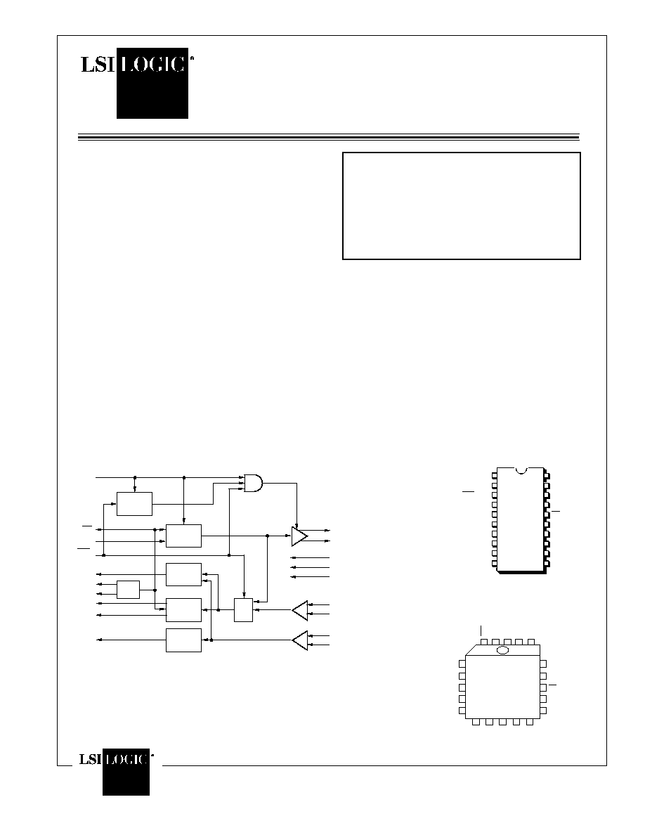
Figure 1. 8020 MCC Manchester Code Converter
Block Diagram.
Functional Block Diagram
RxD
GND
COLL≠
COLL+
X2
9
10
11
12
13
2
GND
1
MODE 1
20
V
CC
19
Tx+
18
Tx≠
17
TxD
15
TxEN
14
X1
Rx+
4
Rx≠
5
CSN
6
COLL
7
RxC
8
3
LPBK/WDTD
16
TxC
8020
1
2
3
4
5
6
7
8
9
10
20
19
18
17
16
15
14
13
12
11
V CC
Tx+
Tx≠
MODE 1
GND
Rx+
Rx≠
CSN
COLL
RxC
RxD
VSS
TxD
TxEN
X1
X2
COLL+
COLL≠
LPBK/WDTD
TxC
TxEN
CSN
X1
X2
RxC
RxD
COLL
TRANSMIT
Tx+
Tx≠
RECEIVE
Rx+
Rx≠
COLL+
COLL≠
COLLISION
TxC
TxD
LPBK/
WDTD
WATCHDOG
TIMER
ENCODER
CARRIER
SENSE
DECODER
10MHz
DETECTOR
XTAL
CLOCK
MUX
VCC
VSS
MODE 1
DUAL-IN LINE
TOP VIEW
Note: Check for latest Data Sheet revision
before starting any designs.
SEEQ Data Sheets are now on the Web, at
www.lsilogic.com.
This document is an LSI Logic document. Any
reference to SEEQ Technology should be
considered LSI Logic.

8020
2
MD400023/D
The SEEQ 8020 MCC is a functionally complete Encoder/
Decoder including ECL level balanced driver and receiv-
ers, on board oscillator, analog phase locked loop for clock
recovery and collision detection circuitry. In addition, the
8020 includes a watchdog timer, a 4.5 microsecond win-
dow generator, and a loopback mode for diagnostic opera-
tion.
Together with the 8003 or 8005 and a transceiver, the 8020
Manchester Code Converter provides a high performance
minimum cost interface for any system to Ethernet.
Functional Description
The 8020 Manchester Code Converter chip has two por-
tions, transmitter and receiver. The transmitter uses
Manchester encoding to combine the clock and data into
a serial stream. It also differentially drives up to 50 meters
of twisted pair transmission line. The receiver detects the
presence of data and collisions. The 8020 MCC recovers
the Manchester encoded data stream and decodes it into
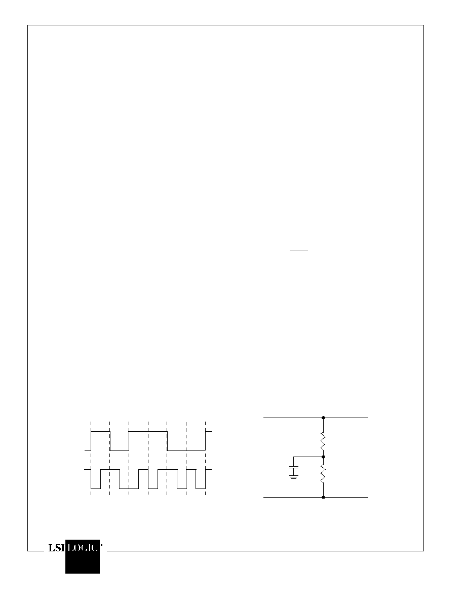
clock and data outputs. Manchester Encoding is the
process of combining the clock and data stream so that
they may be transmitted on a single twisted pair of wires,
and the clock and data may be recovered accurately upon
reception. Manchester encoding has the unique property
of a transition at the center of each bit cell, a positive going
transition for a "1", and a negative going transition for a "0"
(See Figure 2). The encoding is accomplished by exclu-
sive-ORing the clock and data prior to transmission, and
the decoding by deriving the clock from the data with a
phase locked loop.
Clock Generator
The internal oscillator is controlled by a 20 MHz parallel
resonant crystal or by an external clock on X1. The 20 MHz
clock is then divided by 2 to generate a 10 MHz
±
0.01%
transmitter clock. Both 10 MHz and 20 MHz clocks are
used in Manchester data encoding.
Figure 3. Differential Input Terminator
Figure 2. Manchester Coding
Manchester Encoder and Differential Output Driver
The encoder combines clock and data information for the
transceiver. In Manchester encoding, the first half of the bit
cell contains the complement of the data and the second
half contains the true data. Thus a transition is always
guaranteed in the middle of a bit cell.
Data encoding and transmission begin with TxEN going
active; the first transition is always positive for Tx(-) and
negative for Tx(+). In IEEE mode, at the termination of a
transmission, TxEN goes inactive and transmit pair ap-
proach to zero differential. In Ethernet mode, at the end of
the transmission, TxEN goes inactive and the transmit pair
stay differentially high. The transmit termination can occur
at bit cell center if the last bit is a one or at a bit boundary
if the last bit is a zero. To eliminate DC current in the
transformer during idle, Tx
±
is brought to 100 mV differen-
tial in 600 ns after the last transition (IEEE mode). The
back swing voltage is guaranteed to be less than .1 V.
Watchdog Timer
A watchdog timer is built on chip. It can be enabled or
disabled by the LPBK/WDTD signal. The timer starts
counting at the beginning of the transmission. If TxEN
goes inactive before the timer expires, the timer is reset
and ready for the next transmission. If the timer expires
before the transmission ends, transmission is aborted by
disabling the differential transmitter. This is done by idling
the differential output drivers (differential output voltage
becomes zero) and deasserting CSN.
Differential Input Circuit (Rx+ and Rx≠, COLL+ and
COLL≠).
As shown in Figure 3, the differential input for Rx+ and Rx-
and COLL+ and COLL- are externally terminated by a pair
of 39.2
±
1% resistors in series for proper impedance
matching.
SERIAL
DATA
TRANSMITTED
DATA
(MANCHESTER
ENCODED)
1
0
1
1
0
0
COLLISION OR
RECEIVE
INPUT
0.01 µF
39.2 ± 1%
TRANSCEIVER
CABLE
39.2
± 1%
+
≠

8020
3
MD400023/D
The center tap has a 0.01
µ
F capacitor, tied to ground, to
provide the AC common mode impedance termination for
the transceiver cable.
Both collision and receiver input circuits provide a static
noise margin of -140 mV to -300mV (peak value). Noise
rejection filters are provided at both input pairs to prevent
spurious signals. For the receiver pair, the range is 15 ns
to 30 ns. For the collision pair, the range is 10 ns to 18 ns.
The D.C. threshold and noise rejection filter assure that
differential receiver data signals less than -140 mV in
amplitude or narrower than 15 ns (10 ns for collision pair)
are always rejected, signals greater than -300 mV and
wider than 30 ns (18 ns for collision pair) are always
accepted.
Manchester Decoder and Clock Recovery Circuit
The filtered data is processed by the data and clock
recovery circuit using a phase-locked loop technique. The
PLL is designed to lock onto the preamble of the incoming
signal with a transition width asymmetry not greater than
+8.25 ns to -8.25 ns within 12 bit cell times worst case and
can sample the incoming data with a transition width
asymmetry of up to +8.25 ns to -8.25 ns. The RxC high or
low time will always be greater than 40 ns. RxC follows
TxC for the first 1.2
µ
s and then switches to the recovered
clock. In addition, the Encoder/Decoder asserts the CSN
signal while it is receiving data from the cable to indicate
the receiver data and clock are valid and available. At the
end of the frame, after the node has finished receiving,
CSN is deasserted and will not be asserted again for a
period of 4.5
µ
s regardless of the state of the state of the
receiver pair or collision pair. This is called inhibit period.
There is no inhibit period after packet reception. During
clock switching, RxC may stay high for 200ns maximum.
Collision Circuit
A collision on the Ethernet cable is sensed by the trans-
ceiver. It generates a 10 MHz
±
15% differential square
wave to indicate the presence of the collision. During the
collision period, CSN is asserted asynchronously with
RxC. However, if a collision arrives during inhibit period
4.5
µ
s from the time CSN was deasserted, CSN will not be
reasserted.
Loopback
In loopback mode, encoded data is switched to the PLL
instead of Tx+/Tx- signals. The recovered data and clock
are returned to the Ethernet Controller. All the transmit and
receive circuits, including noise rejection filter, are tested
except the differential output driver and the differential
input receiver circuits which are disabled during loopback.
At the end of frame transmission, the 8020 also generates
a 650 ns long COLL signal 550 ns after CSN was deas-
serted to simulate the IEEE 802.3 SQE test. The watchdog
timer remains enabled in this mode.
Pin Description
The MCC chip signals are grouped into four categories:
∑ Power Supply and Clock
∑ Controller Interface
∑ Transceiver Interface
∑ Miscellaneous
Power Supply
V
CC
..........................................................................+5V
V
SS
.....................................................................Ground
X1 and X2 clock (Inputs): Clock Crystal: 20 MHz crystal
oscillator input. Alternately, pin X1 may be used at a TTL
level input for external timing by floating pint X2,
Controller Interface
RxC Receive Clock (Output): This signal is the recov-
ered clock from the phase decoder circuit. It is switched to
TxC when no incoming data is present from which a true
receive clock is derived. 10 MHz nominal and TTL compat-
ible.
RxD Receive Data (Output): The RxD signal is the
recovered data from the phase decoder. During idle
periods, the RxD pin is LOW under normal conditions. TTL
and MOS level compatible. Active HIGH.
CSN Carrier Sense (Output): The Carrier Sense Signal
indicates to the controller that there is activity on the
coaxial cable. It is asserted when receive data is present
or when a collision signal is present. It is deasserted at the
end of frame or at the end of collision, whichever occurs
later. It is asserted or deasserted synchronously with RxC.
TTL compatible.
TxC Transmit Clock (Output): A 10 MHz signal derived
from the internal oscillator. This clock is always active.
TTL and MOS level compatible.
TxD Transmit Data (Input): TxD is the NRZ serial input
data to be transmitted. The data is clocked into the MCC
by TxC. Active HIGH, TTL compatible.

8020
4
MD400023/D
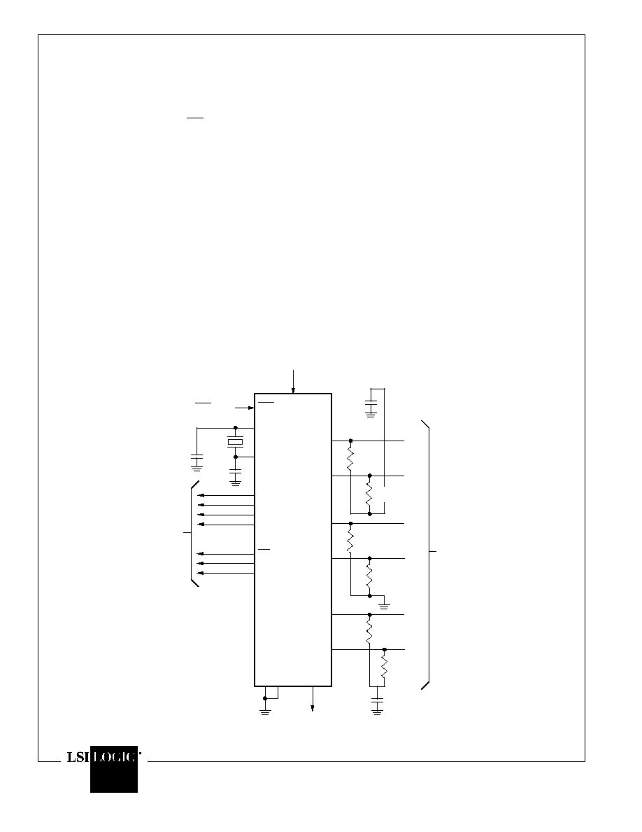
Figure 4. 8020 Interface
TxEN Transmit Enable (Input): Transmit Enable, when
asserted, enables data to be sent to the cable. It is
asserted synchronously with TxC. TxEN goes active with
the first bit of transmission. TTL compatible.
COLL Collision (Output): When asserted, indicates to
the controller the simultaneous transmission of two or
more stations on network cable. TTL Compatible.
Transceiver Interface
Rx+ and Rx≠ Differential Receiver Input Pair (Input):
Differential receiver input pair which brings the encoded
receive data to the 8020. The last transition is always
positive-going to indicate the end of the frame.
COLL+ and COLL≠ Differential Collision Input Pair
(Input): This is a 10 MHz
±
15% differential signal from the
transceiver indicating collision. The duty cycle should not
be worse than 60%/40% -- 40%/60%. The last transition
is positive-going. This signal will respond to signals in the
range of 5 MHz to 11.5 MHz. Collision signal may be
asserted if `MAU not available' signal is present.
Tx+ and Tx- Differential Transmit Output Pair (Output):
Differential transmit pair which sends the encoded data to
the transceiver. The cable driver buffers are source
follower and require external 243
resistors to ground as
loading. These resistors must be rated at 1 watt to
withstand the fault conditions specified by IEEE 802.3. If
MODE 1=1, after 200 ns following the last transition, the
differential voltage is slowly reduced to zero volts in 8
µ
s
to limit the back swing of the coupling transformer to less
than 0.1 V.
Miscellaneous
MODE 1 (Input): This pin is used to select between AC or
DC coupling. When it is tied high or left floating, the output
drivers provide differential zero signal during idle (IEEE
802.3 specification). When pin 1 is tied low, then the
output is differentially high when idle (Ethernet Rev.1
specification).
20 MHz
XTAL
20 pF
8003
OR
8005
3
14
13
8
9
6
7
16
17
15
1
MODE 1
X1
X2
RxC
RxD
CSN
COLL
TxD
TxEN
10
20
Rx+
Rx≠
Tx+
Tx≠
COLL+
COLL≠
0.01 µF
4
5
19
18
12
11
39.2
±1%
243
±1%
0.01 µF
39.2
±1%
39.2
±1%
243
±1%
5
12
3
10
2
9
DI-A
DI-B
DO-A
DO-B
CI-A
CI-B
LPBK/WDTD
20 pF
LPBK/
WDTD
TxC
SEEQ
8020
39.2
±1%
+5
2
AUI
CABLE
1W

8020
5
MD400023/D
LPBK/WDTD Loopback /Wat
chdog Timer
Disable (Input):
Normal Operation: For normal operation this pin should
be HIGH or tied to V
CC
. In normal operation the watchdog
timer is enabled.
Loopback: When this pin is brought low, the Manchester
encoded transmit data from TxD and TxC is routed through
the receiver circuit and sent back onto the RxD and RxC
Pins. During loopback, Collision and Receive data inputs
are ignored. The transmit pair is idled. At the end of
transmission, the signal quality error test (SQET) will be
simulated by asserting collision during the inhibit window.
During loopback, the watchdog timer is enabled.
Watchdog Timer Disable: When this pin is between 10 V
(Min.) and 16 V (Max.), the on chip 25 ms Watchdog Timer
will be disabled. The watchdog timer is used to monitor the
transmit enable pin. If TxEN is asserted for too long, then
the watchdog timer (if enabled) will automatically deassert
CSN and inhibit any further transmissions on the Tx+ and
Tx- lines. The watchdog timer is automatically reset each
time TxEN is deasserted.
Interconnection to a Data Link
Controller
Figure 5 shows the interconnections between the 8020
MCC and SEEQ's 8003 or 8005. There are three connec-
tions for each of the two transmission channels, transmit
and receive, plus the Collision Signal line (COLL).
Transmitter connections are:
Transmit Data, TxD
Transmit Clock, TxC
Transmit Enable, TxEN
Collision, COLL
Receiver connections are:
Receive Data, RxD
Receive Clock, RxC
Carrier Sense, CSN
D.C. and A.C. Characteristics and
Timing
Crystal Specification
Resonant Frequency (C
L
= 20 pF) ..................... 20 MHz
±
0.005% 0-70
∞
C
and
±
0.003% at 25
∞
C
Type ................................................. Fundamental Mode
Circuit .............................................. Parallel Resonance
Load Capacitance (C
L
) ........................................... 20pF
Shunt Capacitance (C
O
) ................................... 7pF Max.
Equivalent Series Resistance (R1) ................. 25
Max.
Motional Capacitance (C1) ........................ 0.02 pF Max.
Drive Level ............................................................. 2mW
TxD
TxEN
COLL
RxD
RxC
CSN
LOOPBACK
[1]
TxD
TxEN
LOOPBACK
COLL
RxD
RxC
CSN
8003
OR
8005
8020
MCC
TxC
TxC
Figure 5. Interconnection of 8020 and 8003/8005
NOTE
1. Loopback output on 8005 only.
R1
C1
0
C
L1
EQUIVALENT CIRCUIT OF CRYSTAL
Figure 6.
