DIGITAL LOCK FOR AUTOMOTIVE IGNITIONS
FEATURES:
∑ 5040 Four-Digit Combinations (for a 10 digit Keypad)
∑ Combinations are Hard-Wire Programmed
∑ Sense Input Enables Operation
∑ Save Memory Feature for Valet Parking
∑ Convenience Delay Controlled by External Capacitor
∑ Static or Momentary Lock Control Output
∑ Save Memory and Lock Status Outputs
∑ +5V to +18V Operation (Vss - V
DD
)
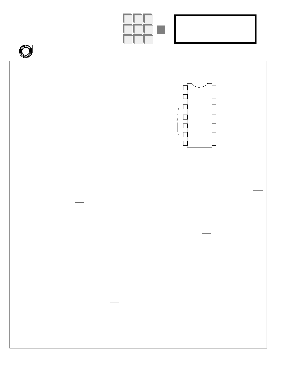
∑ LS7220 (DIP), LS7220-S (SOIC) - See Figure 1
DESCRIPTION:
The LS7220 is a MOS digital lock circuit. When wired to a ten-digit
keypad, the circuit will recognize one four-digit combination out of a
possible 5040 combinations.
The LS7220 is configured with the features required for an Auto-
motive Ignition Anti-Theft Digital Lock (See Figure 5). These
features include Sense input which enables the IC, Save Memory
for Valet Parking, Convenience Delay to maintain Unlock condition
for short term interruptions of the Sense input and Save Status and
Lock Status outputs which can be used for direct drive of LED
indicators.
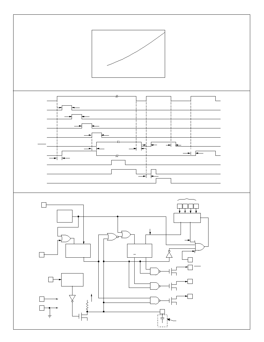
OPERATING DESCRIPTION: (Refer to Figures 2, 3, 4 and 5.)
When the Sense input goes high, the LS7220 is enabled. The Lock
Status output turns on and Save Status and LOCK outputs remain
off. When the programmed four-digit combination is entered from
the keypad, in proper sequence, LOCK turns on and Lock Status
turns off. If the Sense input is interrupted for a period of time great-
er than the Convenience Delay, the operating sequence must start
over. If the Sense input is interrupted for a period of time less than
the Convenience Delay, the operation of the LS7220 is unaffected.
A momentary high at the Save input sets the Save Memory and
causes the LS7220 to save an Unlock condition (Sequential Mem-
ory is set) for any time duration interruption of the Sense input (i.e.,
valet parking). The Save Status output turns on when Save Mem-
ory is set. The Lock input is used to reset the Save Memory and re-
turn the LS7220 to normal operation.
NOTE: Using a 3 x 4 keypad, the
F
key can be connected to the
Lock input and the # key to the Save input. Lock Status and Save
Status outputs can be used to drive red and green LED indicators,
respectively.
INPUT/OUTPUT DESCRIPTION: (Refer to Figure 4)
SENSE INPUT (Pin 1)
A high at this input causes CONVENIENCE DELAY to transition
high and enables recognition of the SELECTED KEYS when they
are inputted in proper sequence. Control logic for LOCK, LOCK
STATUS and SAVE STATUS outputs is also enabled. A low at
this input keeps all outputs off and resets the Sequential Memory if
Save Memory is not set.
V
DD
(Pin 9) Supply voltage negative terminal.
Vss (Pin 14) Supply voltage positive terminal.
1
2
3
4
5
6
7
LSI
14
13
12
11
8
9
10
PIN ASSIGNMENT - TOP VIEW
S E N S E I N
U N S E L E C T E D K E Y S
(RESET)
SELECTED KEYS
(IN SEQUENCE)
LOCK IN
V
SS
(+V)
LOCK OUT
CONVENIENCE
DELAY
SAVE IN
SAVE STATUS OUT
V
DD
(-V)
LOCK STATUS OUT
FIGURE 1.
LS 7220
I
1
I
2
I
3
I
4
7220-012703-1
January 2003
UNSELECTED KEYS (RESET) INPUT (Pin 2)
A high at this input resets the Sequential Detector for the
SELECTED KEYS inputs. This input must be wired to all digit keys
which are not part of the Four-Digit Combination.
SELECTED KEYS INPUTS (Pins 3, 4, 5, 6)
When these inputs are brought high in correct sequence, (i.e.,I1, I2,
I3, I4) the Sequential Memory is set if SENSE input is high. LOCK
output turns on and LOCK STATUS output turns off when the
Sequential Memory is set.
LOCK INPUT (Pin 7)
A high at this input resets the Save Memory. The SAVE STATUS
output turns off when this occurs.
LOCK STATUS OUTPUT (Pin 8)
This output is the complement of LOCK output when the SENSE
input is high. See NOTE.
SAVE STATUS OUTPUT (Pin 10)
This output turns on when Save Memory is set and SENSE input is
high. See NOTE.
SAVE INPUT (Pin 11)
A high at this input sets the Save Memory. If Save Memory is set
and Sequential Memory is set, the Save Memory will prevent the
Sequential Memory from being reset as a result of a change at the
SENSE Input. (See SAVE STATUS OUTPUT.)
CONVENIENCE DELAY I/O (Pin 12)
An external capacitor placed on this pin will delay the effect of
changes at the SENSE Input from affecting the outputs and the
condition of the Sequential Detector and Sequential Memory.
(See Figure 2)
LOCK OUTPUT (Pin 13)
This output turns on when the Sequential Memory is set and
SENSE input is high. See NOTE.
NOTE: Outputs are off when SENSE input is low.
LSI/CSI
LSI Computer Systems, Inc. 1235 Walt Whitman Road, Melville, NY 11747 (631) 271-0400 FAX (631) 271-0405
LS7220
UL
Æ
A3800

ABSOLUTE MAXIMUM RATINGS:
PARAMETER
SYMBOL
VALUE
UNIT
DC Supply Voltage V
SS
- V
DD
+20
V
Any Input Voltage
V
IN
V
SS
- 20 to V
SS
+ 0.5
V
Operating Temperature T
A
-25 to +85
∞C
Storage Temperature
T
STG
-65 to +150
∞C
TRANSIENT CHARACTERISTICS: (See Figure 3)
(T
A
= -25∞C to +85∞C, V
SS
= +5V to +18V)
PARAMETER
SYMBOL
MIN
MAX
UNIT
CONDITION
SENSE High Delay to
T
SE
-
1
µs
No external
Outputs Enabled
capacitor, Pin 12
SENSE Low Delay to
T
SD
-
10
µs
No external
Outputs Disabled
capacitor, Pin 12
Input Pulse Widths
T
PW
25
-
µs
-
(except SENSE)
Valid Combination Entry to
T
CE
-
10
µs
SENSE High
LOCK Output Enabled
7220-012703-2
DC ELECTRICAL CHARACTERISTICS:
(All voltages referenced to V
DD
; T
A
= -25∞C to +85∞C unless otherwise specified.) Vss voltages = 5V, 9V, 12V, 15V, 18V
PARAMETER SYMBOL MIN MAX UNIT CONDITION
Supply Voltage
V
SS
+5
+18
V
-
Supply Current
I
SS
-
20, 30, 40, 50, 70
µA
V
SS
voltages
*INPUT VOLTAGES:
SENSE Low
V
IL
0
2, 3, 4, 6, 8.5
V
V
SS
voltages
SENSE High
V
IH
3.5, 5.5, 6.5, 9, 11.5
V
SS
V
V
SS
voltages
CONVENIENCE DELAY Low
V
IL
-
0.3Vss
-
Typical
CONVENIENCE DELAY High
V
IL
0.7Vss
-
-
Typical
All Other Inputs:
Low
V
IL
0
Vss - 3
V
-
High
V
IH
Vss - 1
Vss
V
-
*NOTE 1: All inputs have pull down resistors to V
DD
. Typical input sink current is 12µA with input at Vss (Vss - V
DD
= +12V)
OUTPUT CURRENT:
***LOCK STATUS
I
O
0.4, 2.5, 5, 9, 14
1.3, 6, 12, 20, **30
mA
Vss voltages
Source Current
Vo = +1.7V
***SAVE STATUS
I
O
0.8, 5, 10, 18, 28
2.6, 12, 24, **30, **30
mA
Vss voltages
Source Current
Vo = +1.7V
CONVENIENCE DELAY
I
O
0.1, 0.5, 0.7, 1, 1.2
0.5, 1.1, 1.6, 2.1, 2.4
mA
Vss voltages
LOCK
I
O
1.3, 6.5, 9.1, 13, 15.6
6.5, 14.7, 21, 27.3, **30
mA
Vss voltages
Inupt Capacitance
C
IN
-
10
pF
-
**NOTE 2: Limit current to 30mA maximum
***NOTE 3: LOCK STATUS and SAVE STATUS output currents are balanced to achieve equal brightness for red and green LEDs

S E N S E I n p u t
I
1
I
2
LOCK
L O C K S T A T U S
S A V E I n p u t
S A V E S T A T U S
LOCK Input
FIGURE 3. LS7220 TIMING DIAGRAM
T
PW
T
PW
T
PW
T
PW
T
CE
T
SE
T
SE
T
SE
T
SE
T
SD
T
SD
I
3
I
4
6
5
4
3
2
13
12
U N S E L E C T E D
KEYS (RESET)
S E Q U E N T I A L
D E T E C T O R
INCORRECT
S E Q U E N C E
C O R R E C T
S E Q U E N C E
S E Q U E N T I A L
MEMORY
P O W E R
ON
R E S E T
S A V E
MEMORY
LOGIC "1"
L E V E L
R E S T O R E
LOCK
LOCK STATUS
8
10
S A V E S T A T U S
CONVENIENCE DELAY
-
+
V
SS
C
SELECTED KEYS (IN SEQUENCE)
I
1
I
2
I
3
I
4
1
14
9
V
SS
V
DD
(+V)
(-V)
V
SS
V
SS
V
SS
V
SS
V
DD
11
7
R
S
Q
R
S
Q
Q
S A V E
INPUT
LOCK
INPUT
Capacitor
Discharge
Current
FIGURE 4. LS7220 BLOCK DIAGRAM
S E N S E
INPUT
(ENABLE)
R
External Capacitor
FIGURE 2. CONVENIENCE DELAY TIME vs POWER SUPPLY
(with External Capacitor C, Pin 12)
T
SD
, seconds
Typical Curve for C = 5µF
T
A
= 25
∞
C
(V
SS-
V
DD
), Volts
5
10
15
18
8
4
6
2
14
0
12
10
7220-012703-3

SEE NOTE 2
(CONVENIENCE DELAY)
FROM
IGNITION
SWITCH
C (See Note 1)
+12V
SENSE IN
VSS
UNSELECTED
KEYS (RESET)
I
1
I
2
I
3
I
4
LOCK IN
LOCK
CONVENIENCE
DELAY
SAVE IN
SAVE
STATUS
V
DD
LOCK
STATUS
GREEN LED (SAVE INDICATIOR)
RED LED (LOCK INDICATOR)
C1 (See Note 2)
RELAY
COIL
(UNLOCK RELAY)
+12V
.05
µ
F,25V
+12V
FIGURE 5. TYPICAL ANTI-THEFT DIGITAL LOCK
LS7220
.05
µ
F
250V
KEYPAD
1
2
3
4
5
6
7
8
9
10
11
12
13
14
Note 1: C is optional. It may be required to prevent ignition noise from
generating a false reset. (Typical values range from 0.1µF to 0.47µF)
Note 2: See Figure 2 to select C1 value for desired Convenience Delay Time.
If Convenience Delay is not desired, wire Keypad to +12V instead of
CONVENIENCE DELAY and eliminate C1.
To
Starter
Solenoid
or
Starter
Motor
or
Hood Lock
NC
NO
+12V
-
+
A typical automotive anti-theft digital lock circuit is shown in Figure 5.
When the Ignition Switch is turned on the SENSE input (Pin 1) goes high
and the circuit is ready to accept the unlocking input sequence at I1, I2, I3
and I4 (Pins 3, 4, 5 and 6, respectively). If the keys associated with these
inputs are depressed exactly in sequence, the LOCK output (Pin 13) turns
ON and the Unlock Relay is energized. This state is indicated by the OFF
condition of the LOCK STATUS output (Pin 8) which turns the red LED
OFF (indicates unlock condition). If the keys are depressed in any se-
quence other than as described above, the internal sequential detector re-
sets and the entire sequence must be repeated (See Figure 4).
V
SS
UNSELECTED
KEYS
I
1
I
2
I
3
I
4
CONVENIENCE
DELAY
V
DD
+12V
-
+
C1 (See Note 1)
L S 7 2 2 0
1
2
3
4
5
6
7
8
9
10
11
12
13
14
TO
LOCK CONTROL
CIRCUIT
NOTE 1:
C1 value determines the
Combination Entry Time and
duration of Momentary LOCK
Output (See Figure 4). Select
C1 value from Figure 2. Code
shown is 4179.
See Note 1
S e e
Note 1
0
1
2
3
4
5
6
7
8
9
.
0 5 µ F
FIGURE 6. DIGITAL LOCK WITH MOMENTARY OUTPUT
LOCK
KEYPAD
+12V
In order to save the ON condition of the LOCK output before the ignition switch
is turned Off (i.e., when the SENSE input becomes low) the key associated with
the SAVE input (Pin 11) has to be depressed. The "SAVE" status is indicated
by a high at the SAVE STATUS output (Pin 10), which turns the green LED On.
If the ignition switch is turned Off when the green LED is On, all the output stat-
us are preserved in the internal memory, so that when the ignition switch is
turned on again there is no need to go through the input sequence again. This
feature could be used for valet parking and garage service.
Status saving may be cancelled by depressing the LOCK input key followed by
turning the ignition switch Off for a time greater than the CONVENIENCE
DELAY (See Figure 2). This also turns OFF the LOCK output.
7220-012703-4


