DEVICES INCORPORATED
LF3311
Horizontal / Vertical Digital Image Filter
Improved Performance
LOGIC Devices Incorporated
1
Dec 18, 2001 LDS.3311-A
Video Imaging Products
111 MHz Data Rate
12-bit Data and Coefficients
On-board Memory for 256 Horizontal and 256 Verti-
cal Coefficient Sets
LF InterfaceTM Allows All 512 Coefficient Sets to be
Updated Within Vertical Blanking
Selectable 12-bit Data Output with User-Defined
Rounding and Limiting
Seven 3K x 12-bit, Programmable Two-Mode Line
Buffers
16 Horizontal Filter Taps
8 Vertical Filter Taps
Two Operating Modes: Dimensionally Sepa-
rate and Orthogonal
Supports Interleaved Data Streams
Horizontal Filter Supports Decimation up to
16:1 for Increasing Number of Filter Taps
3.3 Volt Power Supply
5 Volt Tolerant I/O
144 Lead PQFP
The LF3311 is an improved version of the LF3310 Horizontal/Vertical Digital Image Filter capable of
operating at speeds of up to 111MHz. This improved speed will increase flexibility and performance. The
added performance will enable you to use this device in more applications. For example, four interleaved
data streams of 27MHz can now be processed within one device. The part is functionally identical to the
LF3320 with the exception that the filter data path is specified to operate faster than the LF Control Interface.
When operating the filter at speeds in excess of 90MHz, loading of coefficients via the LF Interface must
be throttled to a maximum of 90MHz by asserting the PAUSE pin as required to allow sufficient setup time
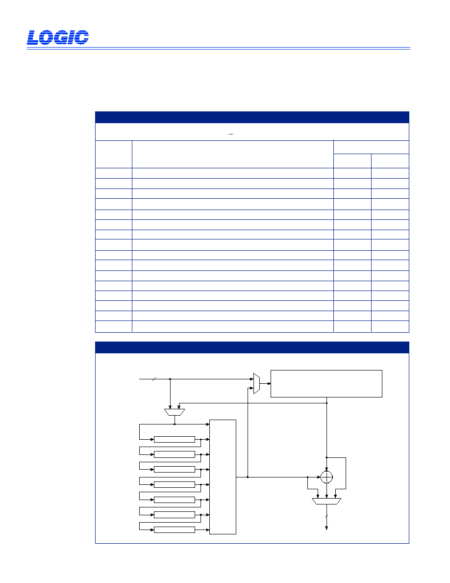
for the configuration data provided to the Figure 1 below demonstrates the switching waveforms of case 2,
while the switching characteristics are shown in Table 1.
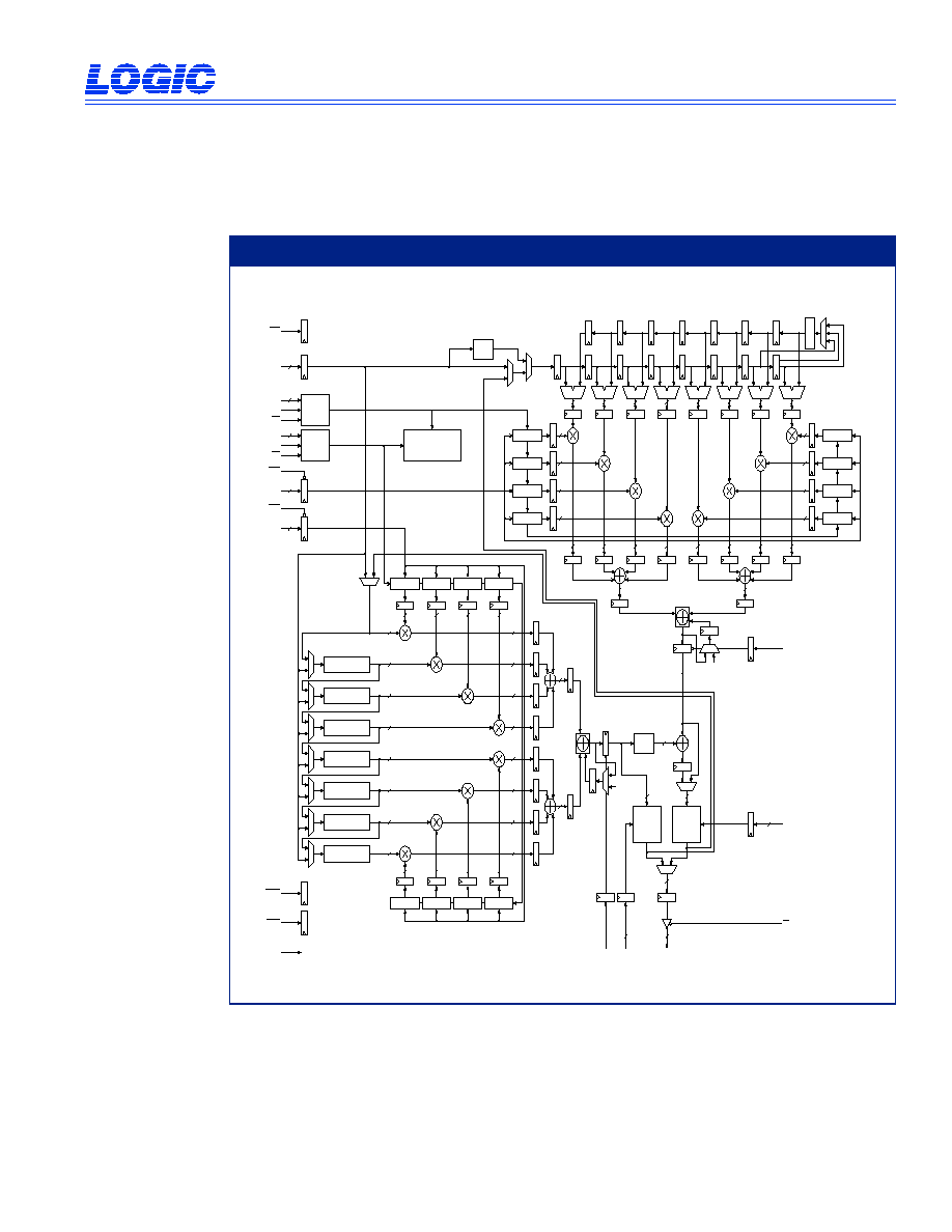
The LF3311 remains a two-dimensional digital image filter capable of filtering data at real-time video rates.
The device contains both a horizontal and a vertical filter which may be cascaded or used concurrently for
two-dimensional filtering. The input, coefficient, and output data are all 12-bits and in two's complement
format. The horizontal filter is designed to take advantage of symmetric coefficient sets. When symmetric
coefficient sets are used, the horizontal filter can be configured as a 16-tap FIR filter. When asymmetric
coefficient sets are used, it can be configured as an 8-tap FIR filter. The vertical filter is an 8-tap FIR
filter with all required line buffers contained on-chip. The line buffers can store video lines with lengths
from 4 to 3076 pixels. Horizontal filter Interleave/Decimation Registers (I/D Registers) and the vertical filter
line buffers allow interleaved data to be fed directly into the device and filtered without separating the data
into individual data streams. The horizontal filter can handle a maximum of sixteen data sets interleaved
together. The vertical filter can handle interleaved video lines which contain 3076 or less data values. The
I/D Registers and horizontal accumulator facilitate using decimation to increase the number of filter taps
in the horizontal filter. It will support a decimation factor of up to 16:1. The device has on-chip storage
for 256 horizontal coefficient sets and 256 vertical coefficient sets. Each filter's coefficients are loaded
independently of each other allowing one filter's coefficients to be updated without affecting the other filter's
coefficients. In addition, a horizontal or vertical coefficient set can be updated independently from the other
coefficient sets in the same filter.
FEATURES
DESCRIPTION
Figure 1. Switching Waveforms: LF Interface
TM
tS0
tCFS
tPWH
tCYC
tPWL
ADDRESS
tPH
PAUSEA
PAUSEB
CFA 11-0
CFB 11-0
tLH
CLK
LDA
LDB
tCFH
tPS
CF0
CF1

DEVICES INCORPORATED
LF3311
Horizontal / Vertical Digital Image Filter
Improved Performance
LOGIC Devices Incorporated
2
Dec 18, 2001 LDS.3311-A
Video Imaging Products
DIN
11-0
3K LINE BUFFER
12
DOUT
11-0
12
256 COEFFICIENT SET STORAGE
256 COEFFICIENT SET STORAGE
16-TAP HORIZONTAL FILTER
8-TAP VERTICAL FILTE
R
3K LINE BUFFER
3K LINE BUFFER
3K LINE BUFFER
3K LINE BUFFER
3K LINE BUFFER
3K LINE BUFFER
Figure 2. LF3311 Block Diagram
Symbol
Parameter
MIN
MAX
t
CYC
Cycle Time
9
t
PWL
Clock Pulse Width Low
4
t
PWH
Clock Pulse Width High
4
t
S0
Input Setup Time
4
t
S1
Input Setup Time (xCEN, xRSL)
4
t
H0
Input Hold Time
1
t
H1
Input Hold Time (xCEN, xRSL)
1.5
t
D
Output Delay
8
t
DIS
Three-State Output Disable Delay
10
t
ENA
Three-State Output Enable Delay
10
t
CFS
Coefficient Input Setup Time
5
t
CFH
Coefficient input Hold Time
1.5
t
LS
Load Setup Time
4
t
LH
Load Hold Time
1.5
t
PS
PAUSE Setup Time
4
t
PH
PAUSE Hold time
1.5
Table 1. Switching Characteristics
Commercial Operating Range (0�C to + 70�C)
9 (ns) speed grade

DEVICES INCORPORATED
LF3311
Horizontal / Vertical Digital Image Filter
Improved Performance
LOGIC Devices Incorporated
3
Dec 18, 2001 LDS.3311-A
Video Imaging Products
DIN
11-0
3K Line Buffer
DOUT
11-0
12
32
12
12
12
12
V Coef Bank 7
V Coef Bank 6
V Coef Bank 5
V Coef Bank 4
12
V Coef Bank 0
12
V Coef Bank 1
12
V Coef Bank 2
12
V Coef Bank 3
3K Line Buffer
3K Line Buffer
3K Line Buffer
3K Line Buffer
3K Line Buffer
3K Line Buffer
24
24
24
24
24
24
24
24
26
26
12
VCA
7-0
VCEN
8
12
12
12
12
12
12
12
12
VSHEN
"0"
VACC
OE
ALU
A
B
ALU
A
B
ALU
A
B
ALU
A
B
ALU
A
B
ALU
A
B
ALU
A
B
ALU
A
B
13
H Coef Bank 0
12
H Coef Bank 1
12
H Coef Bank 2
12
H Coef Bank 3
12
13
13
13
13
13
13
13
H Coef Bank 7
12
H Coef Bank 6
12
H Coef Bank 5
12
H Coef Bank 4
12
25
25
25
25
25
25
25
25
27
27
HCA
7-0
HCEN
8
"0"
HACC
DATA
DELAY
HSHEN
CLK
DATA
DELAY
1-16
1-16
1-16
1-16
1-16
1-16
1-16
1-16
1-16
1-16
1-16
1-16
1-16
1-16
I
E
O
DAT
A
REVERSAL
1-16
HORIZONTAL
LF
INTERFACE
HCF
11-0
HLD
12
VERTICAL
LF
INTERFACE
VCF
11-0
VLD
12
TXFR
ROUND
SELECT
LIMIT
12
32
VRSL
3-0
4
HRSL
3-0
4
32
32
CONFIGURATION AND
CONTROL REGISTERS
VERTICAL
ROUND
SELECT
LIMIT
HORIZONTAL
I/D REGISTERS
HPAUSE
VPAUSE
Figure 3. LF3311 Functional Block Diagram

DEVICES INCORPORATED
LF3311
Horizontal / Vertical Digital Image Filter
Improved Performance
LOGIC Devices Incorporated
4
Dec 18, 2001 LDS.3311-A
Video Imaging Products
The horizontal filter is designed to filter a digital image in the horizontal dimension. This FIR filter can
be configured to have as many as 16-taps when symmetric coefficient sets are used and 8-taps when
asymmetric coefficient sets are used.
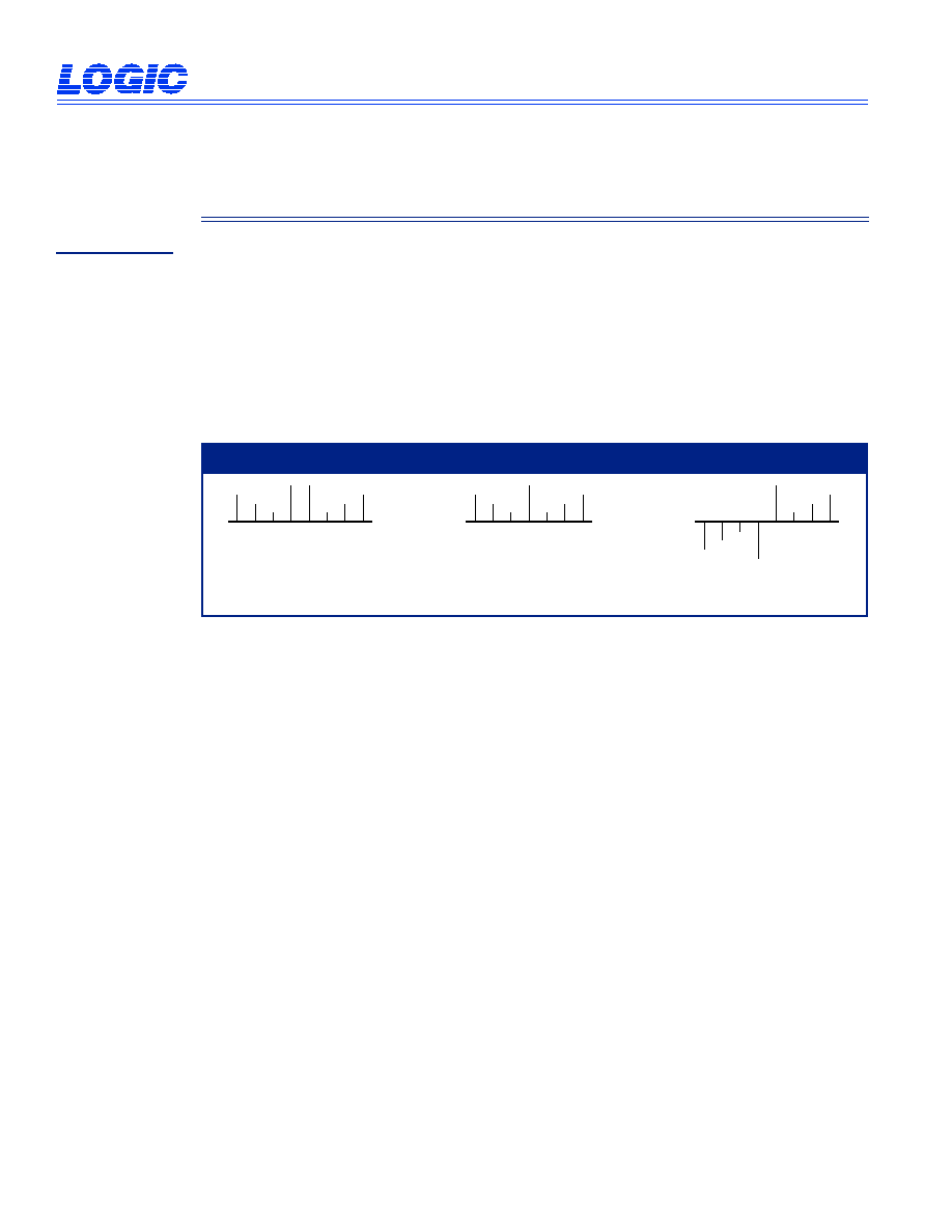
The ALUs double the number of filter taps available, when symmetric coefficient sets are used, by pre-
adding data values which are then multiplied by a common coefficient (see Figure 4). The ALUs can
perform two operations: A+B and B�A. Bit 0 of Configuration Register 0 determines the ALU operation.
A+B is used with even-symmetric coefficient sets. B�A is used with odd-symmetric coefficient sets. Also,
either the A or B operand may be set to 0. Bits 1 and 2 of Configuration Register 0 control the ALU inputs.
A+0 or B+0 are used with asymmetric coefficient sets.
The Interleave/Decimation Registers (I/D Registers) feed the ALU inputs. They allow the device to filter up
to sixteen data sets interleaved into the same data stream without having to separate the data sets. The I/D
Registers should be set to a length equal to the number of data sets interleaved together. For example, if
two data sets are interleaved together, the I/D Registers should be set to a length of two. Bits 1 through 4 of
Configuration Register 1 determine the I/D Register length.
The I/D Registers also facilitate using decimation to increase the number of filter taps. Decimation by N
is accomplished by reading the horizontal filter's output once every N clock cycles. The device supports
decimation up to 16:1. With no decimation, the maximum number of filter taps is sixteen. When decimating
by N, the number of filter taps becomes 16N because there are N�1 clock cycles when the horizontal filter's
output is not being read. The extra clock cycles are used to calculate more filter taps.
When decimating, the I/D Registers should be set to a length equal to the decimation factor. For example,
when performing a 4:1 decimation, the I/D Registers should be set to a length of four. When not decimating
or when only one data set (non-interleaved data) is fed into the device, the I/D Registers should be set
to a length of one.
HSHEN enables or disables the loading of data into the forward and reverse I/D Registers when the device
is in Dimensionally Separate Mode (see the HSHEN section for a full discussion). When in Orthogonal
Mode, HSHEN also enables or disables the loading of data into the input register (DIN11-0) and the line
buffers.
It is important to note that in Orthogonal Mode, either HSHEN or VSHEN can disable the loading of data
into the input register (DIN11-0), I/D Registers, and line buffers. Both must be active to enable data loading
in Orthogonal Mode.
Functional Description
Horizontal Filter
ALU
I/D Registers
1
2
3
4
5
6
7
8
Even-Tap, Even-Symmetric
Coefficient Set
Odd-Tap, Even-Symmetric
Coefficient Set
1
2
3
4
5
6
7
8
Even-Tap, Odd-Symmetric
Coefficient Set
1
2
3
4
5
6
7
Figure 4. Symmetric Coefficient Set Examples

DEVICES INCORPORATED
LF3311
Horizontal / Vertical Digital Image Filter
Improved Performance
LOGIC Devices Incorporated
5
Dec 18, 2001 LDS.3311-A
Video Imaging Products
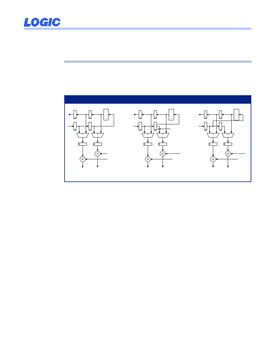
The multiplexer in the middle of the I/D Register data path controls how data is fed to the reverse data path.
The forward data path contains the I/D Registers in which data flows from left to right in the block diagram in
Figure 1. The reverse data path contains the I/D Registers in which data flows from right to left. When the
filter is configured for an even number of taps, data from the last I/D Register in the forward data path is fed
into the first I/D Register in the reverse data path (see Figure 5).
When the filter is configured for an odd number of taps, the data which will appear at the output of the last
I/D Register in the forward data path on the next clock cycle is fed into the first I/D Register in the reverse
data path. Bit 5 in Configuration Register 1 configures the filter for an even or odd number of taps.
When interleaved data is fed through the device and an even tap filter is desired, the filter should be
configured for an even number of taps (Bit 5 of CR1 set to "0") and the I/D Register length should match
the number of data sets interleaved together. When interleaved data is to be fed through the device and
an odd tap filter is desired, the filter should be set to Odd-Tap Interleave Mode. Bit 0 of Configuration
Register 1 configures the filter for Odd-Tap Interleave Mode. When the filter is configured for Odd-Tap
Interleave Mode, data from the next to last I/D Register in the forward data path is fed into the first I/D
Register in the reverse data path.
When the filter is configured for an odd number of taps (interleaved or non-interleaved modes), the filter is
structured such that the center data value is aligned simultaneously at the A and B inputs of the last ALU in
the forward data path. In order to achieve the correct result, the user must divide the coefficient by two.
Data reversal circuitry is placed after the multiplexer which routes data from the forward data path to the
reverse data path (see Figure 6). When decimating, the data stream must be reversed in order for data to be
properly aligned at the inputs of the ALUs. When data reversal is enabled, the circuitry uses a pair of LIFOs
to reverse the order of the data sent to the reverse data path. When TXFR goes LOW, the LIFO sending
data to the reverse data path becomes the LIFO receiving data from the forward data path, and the LIFO
receiving data from the forward data path becomes the LIFO sending data to the reverse data path. The
device must see a HIGH to LOW transition of TXFR in order to switch LIFOs. If decimating by N, TXFR
should go low once every N clock cycles. When data reversal is disabled, the circuitry functions like an
I/D Register. When feeding interleaved data through the filter, data reversal should be disabled. Bit 6 of
Configuration Register 1 enables or disables data reversal.
Functional Description
ALU
A
B
ALU
A
B
COEF 7
COEF 6
1-16
1-16
1-16
1-16
DAT
A
REVERSAL
ALU
A
B
ALU
A
B
COEF 7
COEF 6
1-16
1-16
1-16
1-16
DAT
A
REVERSAL
Delay Stage N 1
ALU
A
B
ALU
A
B
COEF 6
1-16
1-16
1-16
1-16
DAT
A
REVERSAL
EVEN-TAP MODE
ODD-TAP MODE
ODD-TAP INTERLEAVE MODE
2
COEF 7
2
Delay Stage N
Figure 5. I/D Register Data Paths
I/D Register Data
Path Control
Data Reversal

