 | –≠–ª–µ–∫—Ç—Ä–æ–Ω–Ω—ã–π –∫–æ–º–ø–æ–Ω–µ–Ω—Ç: ACR300SE | –°–∫–∞—á–∞—Ç—å:  PDF PDF  ZIP ZIP |

www.dynexsemi.com
ACR300SG33
ACR300SG33
ACR300SG33
ACR300SG33
ACR300SG33
1/6
APPLICATIONS
s
Capacitor Discharge
s
Pulse Power Applications
FEATURES
s
The ACR300SG33 is a high voltage asymmetric
thyristor which has exceptionally fast turn-on
characteristics.
VOLTAGE RATINGS
KEY PARAMETERS
V
DRM
3300V
I
T(AV)
660A
I
TSM
6500A
dVdt 3000V/
µ
s
dI/dt 2000A/
µ
s
t
on
700ns
3300
ACR300SG33
Repetitive Peak
Reverse Voltage
V
RRM
V
20
Lower voltage grades available.
Type Number
Repetitive Peak
Off-state Voltage
V
DRM
V
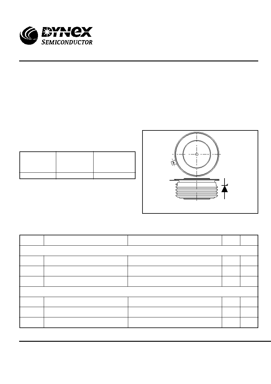
Fig. 1 See Package Details for further information
CURRENT RATINGS
Symbol
Parameter
Conditions
Double Side Cooled
I
T(AV)
Mean on-state current
I
T(RMS)
RMS value
I
T
Continuous (direct) on-state current
Single Side Cooled (Anode side)
I
T(AV)
Mean on-state current
I
T(RMS)
RMS value
I
T
Continuous (direct) on-state current
Units
Max.
Half wave resistive load, T
case
= 80
o
C
660
A
T
case
= 80
o
C
1040
A
T
case
= 80
o
C
890
A
Half wave resistive load, T
case
= 80
o
C
470
A
T
case
= 80
o
C
745
A
T
case
= 80
o
C
570
A
ACR300SG33
Fast Turn-on Asymmetric Thyristor
Replaces April 2000 version, DS5081-2.2
DS5081-2.4 August 2000
Outline type code: G.

www.dynexsemi.com
ACR300SG33
ACR300SG33
ACR300SG33
ACR300SG33
ACR300SG33
2/6
SURGE RATINGS
Conditions
Max.
Units
Symbol
Parameter
I
TSM
Surge (non-repetitive) on-state current
I
2
t
I
2
t for fusing
180
kA
2
s
6
kA
THERMAL AND MECHANICAL DATA
dc
Conditions
Min.
Max.
Units
o
C/W
-
0.070
Anode dc
Clamping force 7.0kN
with mounting compound
Thermal resistance - case to heatsink
R
th(c-h)
0.018
Double side
-
125
o
C
T
vj
Virtual junction temperature
T
stg
Storage temperature range
Reverse (blocking)
Single side
-
Thermal resistance - junction to case
R
th(j-c)
Single side cooled
Symbol
Parameter
Clamping force
6.0
8.0
kN
-55
125
o
C
-
On-state (conducting)
-
150
o
C
-
0.036
o
C/W
o
C/W
Cathode dc
-
0.092
o
C/W
Double side cooled
-
0.042
o
C/W
10ms half sine; T
case
= 125
o
C
V
R
= 0
Fig.1 Turn-on time measurement
V
D
I
G
0.9 x 1600V
0.37 x 1600V
t
t
d
t
r
I
G pk
10% I
G pk
t

www.dynexsemi.com
ACR300SG33
ACR300SG33
ACR300SG33
ACR300SG33
ACR300SG33
3/6
GATE TRIGGER CHARACTERISTICS AND RATINGS
V
DWM
= 12V, R
L
= 6
, T
case
= 25
o
C
Typ.
Max.
Units
Conditions
Parameter
Symbol
V
GT
Gate trigger voltage
V
DWM
= 12V, R
L
= 6
, T
case
= 25
o
C
I
GT
Gate trigger current
-
5
V
-
500
mA
V
FGM
Peak forward gate voltage
-
-
40
V
V
RGM
Peak reverse gate voltage
I
FGM
Peak forward gate current
-
P
GM
Peak gate power
-
-
10
V
-
20
A
-
40
W
-
10
W
-
Forward
Average time 10ms max
P
G(AV)
Average gate power
DYNAMIC CHARACTERISTICS
V
TM
Parameter
Symbol
Conditions
Maximum on-state voltage
At 1000A peak, T
case
= 25
o
C
I
RRM
/I
DRM
Peak reverse and off-state current
At V
RRM
/V
DRM
, T
case
= 125
o
C
From V
DRM
to 125A
Gate source 30V, 10
Gate rise time = 100ns, T
j
= 125∞C
dV/dt
Linear rate of rise of off-state voltage
To V
D
= 2000V, Gate open circuit, T
j
= 125
o
C
Min.
Max.
Units
-
2.0
V
-
60
mA
3000
-
V/
µ
s
-
2000
A/
µ
s
Rate of rise of on-state current
dI/dt
V
T(TO)
Threshold voltage
At T
vj
= 125
o
C
r
T
On-state slope resistance
At T
vj
= 125
o
C
Latching current
1.19
-
V
-
0.81
m
V
D
= 5V, T
j
= 25∞C
I
L
-
600
mA
I
H
Holding current
I
TM
= 500A, I
T
= 5A, T
j
= 25∞C
t
d
Delay time
V
D
= 3000V
Gate source = 30V, 10
Gate rise time = 100ns
-
300
mA
-
350
ns
See Fig.1. T
j
= 25 - 70∞C.
ns
50
-
Rise time
t
r
-
-
ns
T
j
= 25∞C
T
j
= 70∞C
CURRENT CARRYING CAPABILITY AFTER CHIP SHORT CIRCUIT
In the event of a chip short-circuit due to excess anode-cathode
voltage, the device will handle a high continuous RMS fault
current without significant damage. Rating details are as follows:
Continuous current capability: 300A RMS, ac or dc in either
direction.
Conditions:
1. Device single or double side cooled.
2. Case temperature to be held at 200∞C or less.
3. A suitable high temperature clamp to be used.
4. Chip fault site resistance assumed to be 3m
±
10%.

www.dynexsemi.com
ACR300SG33
ACR300SG33
ACR300SG33
ACR300SG33
ACR300SG33
4/6
CURVES
0
500
1000
1500
2000
2500
3000
3500
0
0.5
1
1.5
2
2.5
3
3.5
4
Instantaneous voltage, V
T
- (V)
Instantaneous current, I
T
- (A)
T
j
= 125∞C
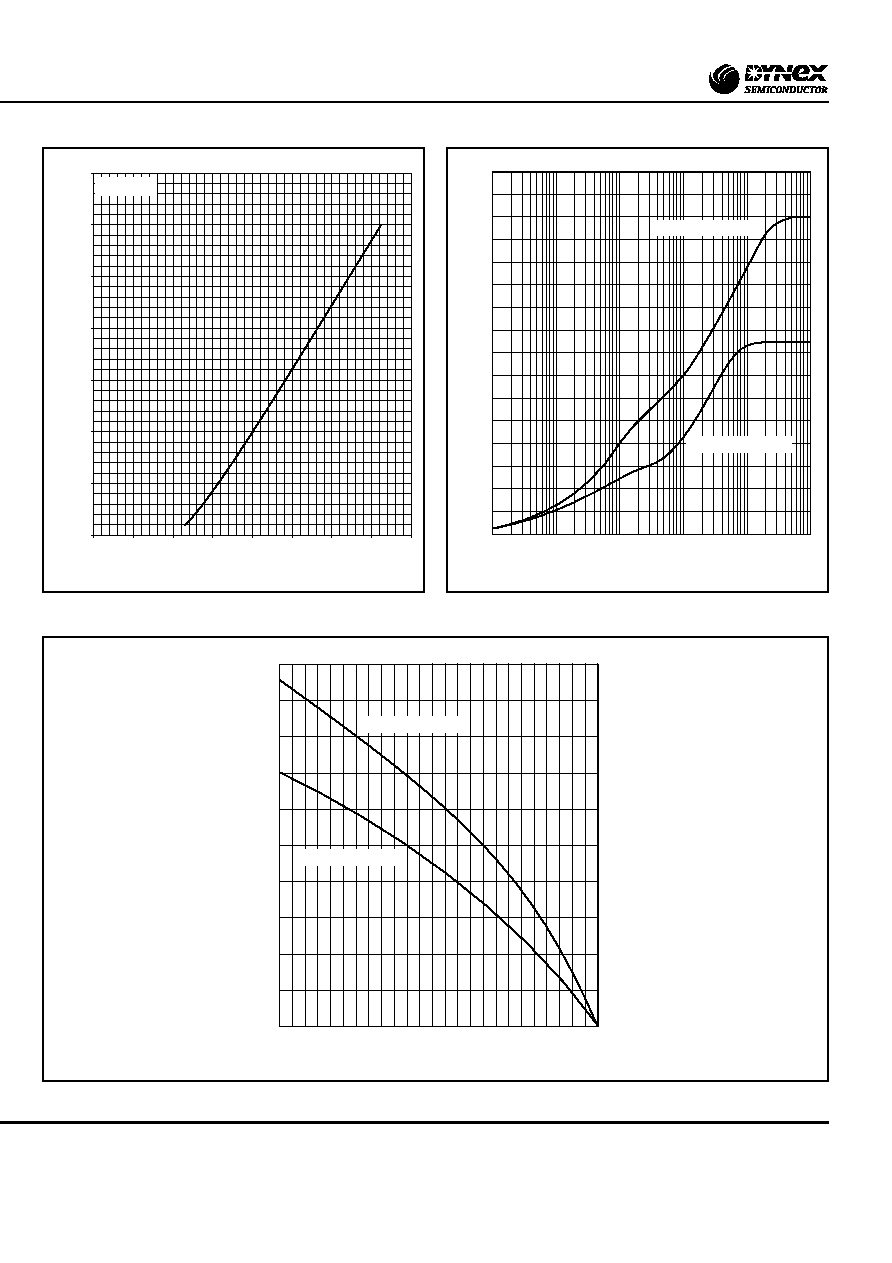
Fig.2 On-state characteristics
Fig.3 Transient thermal impedance - junction to case
0
20
40
60
80
Ther
mal impedance - junction to case
, R
th(j-c)
-
∞
C/kW
0.001
0.01
0.1
1
10
100
Time - (s)
Anode side cooled
Double side cooled
Fig.4 Average current rating vs temperature
25
50
75
100
125
150
Case temperature, T
c
- (∞C)
1000
900
800
700
600
500
400
300
200
100
A
v
er
age current, I
T(A
V
)
- (A)
0
Double side cooled
Anode side cooled

www.dynexsemi.com
ACR300SG33
ACR300SG33
ACR300SG33
ACR300SG33
ACR300SG33
5/6
PACKAGE DETAILS
For further package information, please contact Customer Services. All dimensions in mm, unless stated otherwise.
DO NOT SCALE.
2 holes ÿ3.6x2.0 deep (in both electrodes)
ÿ34 nom
27.0
25.4
ÿ1.5
Cathode
Gate
Anode
ÿ34 nom
ÿ58.5 max
Nominal weight: 310g
Clamping force: 12kN
±
10%
Lead length: 420mm
Lead terminal connector: M4 ring
Package outine type code: G
Cathode tab


