LEM reserves the right to carry out modifications on its transducers without prior notice.
LEM U.S.A., INC.
Page 1 of 2
030516/01
6643 WEST MILL ROAD
TEL: 414/ 353-0711
lus@lem.com
MILWAUKEE, WI 53218
FAX: 414/ 353-0733
http://www.lem.com
C:\aaa\Projects\HTS10P\Rev 01\HTS10P(01).doc 03.05.16 18:11
HTS 10-P Current Transducer
The HTS 10-P provides electronic measurement of AC,
DC, pulsed, and complex currents with galvanic
isolation between the primary (power) circuit and the
secondary (measurement) circuit.
Electrical Data
Nominal Current
10 A
RMS
Measurement Range
± 15 A
Sensitivity
@
25∞C (note 1)
V
DD
∑ 20 = 100 mV/A ± 30%
Overload Capacity
± 25 A for 15 seconds
Supply Voltage (note 1)
5.0 V
DC
± 10%
Primary to Secondary Isolation
2500 V
RMS
for 1 minute
Maximum Output (note 2)
within 500 mV of each supply rail = 0.5 to 4.5 V
Accuracy-Dynamic Performances
Zero Offset
@
25∞C (note 1)
V
DD
/ 2 = 2.5 V
DC
± 12%
Linearity
@
25∞C
< 0.8% typical, 1.2% maximum
Zero Offset Drift
± 2.0 mV/K maximum
Magnetic Offset
± 0.5 % after 45A peak overload
Gain Drift
± 0.20 %/K maximum
Bandwidth, typical
DC - 16 kHz (-3dB; 10 kHz @ -1dB)
Response Time, typical
25 µs (with 2 - 10 A/µs rising or falling edge)
General Data
Operating Temperature
-40 to 85 ∞C
Storage Temperature
-55 to 95 ∞C
Current Consumption
12 mA max
@
5.5V
DC
Output Current (note 3)
1 mA source and sink
Enclosure and Potting
UL Recognized materials meeting UL94-V0
Weight
5 grams nominal
Fastening
PCB Footprint (as shown on page 2)
Output Reference
A positive going output signal is obtained when
the primary current flows from the I+ to I- pin.
Notes:
1) This device is ratiometric: sensitivity and offset vary in direct proportion to supply voltage.
2) Output linearity is not guaranteed within 500mV of the supply rails.
3) Output loading to V
DD
or V
SS
must be = 5.1k
. Tested with 10k
from O
UT
to V
SS
.

LEM reserves the right to carry out modifications on its transducers without prior notice.
LEM U.S.A., INC.
Page 2 of 2
030516/01
6643 WEST MILL ROAD
TEL: 414/ 353-0711
lus@lem.com
MILWAUKEE, WI 53218
FAX: 414/ 353-0733
http://www.lem.com
C:\aaa\Projects\HTS10P\Rev 01\HTS10P(01).doc 03.05.16 18:11
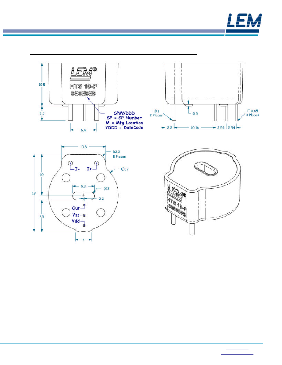
Dimensions for the HTS 10-P in millimeters
(1mm = 0.0394")
:
Notes:
A positive going output signal is obtained when the primary current flows from I+ to I-.
Primary wires may also be used through the aperture. Sensitivity is reduced by a factor of 3.
A positive going output signal is obtained when the primary current flows from bottom to top.
Optimum performance is attained with a 0.1µF capacitor between V
DD
and V
SS
and a 100pF
capacitor between O
UT
to V
SS
, placed as close to the HTS 10-P pins as possible.
Recommended PWB hole diameters: 2 x 1.3 for primary, 3 x 0.8 for secondary.
This device is sensitive to electrostatic discharge (ESD) and must be handled appropriately.

