/home/web/doc/html/kingbright/175887

PHOTOCOUPLER
KB837-B
SPEC NO:DSAD1555
REV NO: V.1 DATE:MAY/05/2003 PAGE: 1 OF 7
APPROVED: J.LU
CHECKED: Tracy Deng DRAWN:Y.H.LI
GENERAL PURPOSE
HIGH ISOLATION VOLTAGE
SINGLE TRANSISTOR TYPE
PHOTOCOUPLER SERIES
APPLICATIONS
1.Computer terminals.
2.Registers,copiers,automatic vending machines.
3.System appliances,measuring instruments.
4.Programmable logic controller.
5.Signal transmission between circuits of different potentials and impedances.
FEATURES
1.Lead forming (gull wing) type, for surface mounting.
2.High isolation voltage between input and output (Viso=5000 Vrms).
3.Compact dual-in-line package
KB837-B: 3-channel type.
4.Recognized by UL and CUL,file NO.E225308.
DESCRIPTION
1.The KB837-B (3-channel) is optically coupled isolators containing a GaAS light emitting
diode and an NPN silicon phototransistor.
2.The lead pitch is 2.54mm.
3.Solid insulation thickness between emitting diode and output phototransistor:>=0.6mm.
PHOTOCOUPLER
KB837-B
SPEC NO:DSAD1555
REV NO: V.1 DATE:MAY/05/2003 PAGE: 2 OF 7
APPROVED: J.LU
CHECKED: Tracy Deng DRAWN:Y.H.LI
*
Absolute Maximum Ratings (T
=
=25
��
��
�
C)
*1
40 to 60% RH,AC for 1 minute.
*2
For 10 seconds.
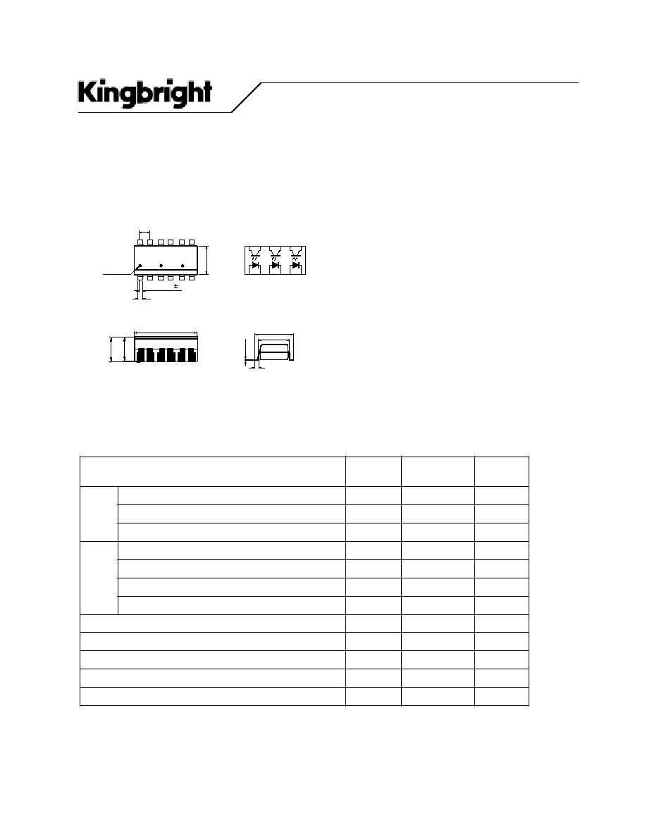
*PACKAGE DIMENSIONS (UNIT:mm)
Lead Bending Type
TOLERANCE
: �
: �
: �
: �
: �
0.5[
�
�
�
�
�
0.02] UNLESS OTHERWISE NOTED.
�
�
.
.
.
.
.
.
.
.
.
.
.
r
e
t
e
m
a
r
a
P
r
e
t
e
m
a
r
a
P
r
e
t
e
m
a
r
a
P
r
e
t
e
m
a
r
a
P
r
e
t
e
m
a
r
a
P
l
o
b
m
y
S
l
o
b
m
y
S
l
o
b
m
y
S
l
o
b
m
y
S
l
o
b
m
y
S
g
n
it
a
R
g
n
it
a
R
g
n
it
a
R
g
n
it
a
R
g
n
it
a
R
ti
n
U ti
n
U ti
n
U ti
n
U ti
n
U
t
u
p
n
I
t
n
e
r
r
u
c
d
r
a
w
r
o
F
I
F
0
5
A
m
e
g
a
tl
o
v
e
s
r
e
v
e
R
V
R
6
V
n
o
it
a
p
i
s
s
i
d
r
e
w
o
P
P
0
7
W
m
t
u
p
t
u
O
e
g
a
tl
o
v
r
e
tt
i
m
e
-
r
o
t
c
e
ll
o
C
V
O
E
C
5
3
V
e
g
a
tl
o
v
r
o
t
c
e
ll
o
c
-
r
e
tt
i
m
E
V
O
C
E
6
V
t
n
e
r
r
u
c
r
o
t
c
e
ll
o
C
I
C
0
5
A
m
n
o
it
a
p
i
s
s
i
d
r
e
w
o
p
r
o
t
c
e
ll
o
C
P
C
0
5
1
W
m
n
o
it
a
p
i
s
s
i
d
r
e
w
o
p
l
a
t
o
T
t
o
t
P
0
0
2
W
m
1
*
e
g
a
tl
o
v
n
o
it
a
l
o
s
I
o
s
i
V
0
0
0
5
s
m
r
V
e
r
u
t
a
r
e
p
m
e
t
g
n
it
a
r
e
p
O
r
p
o
T
0
0
1
+
~
0
3
-
�
C
e
r
u
t
a
r
e
p
m
e
t
e
g
a
r
o
t
S
g
t
s
T
5
2
1
+
~
5
5
-
�
C
2
*
e
r
u
t
a
r
e
p
m
e
t
g
n
ir
e
d
l
o
S
l
o
s
T
0
6
2
�
C
10.0[0.3935]
7.20[0.2835]
0.96[0.038]
7, 9, 11. Emitter
1, 3, 5. Anode
14.74 [0.580]
0.
25[
0.
0
1
]
-0.5
+0.0
KB8
1
7
-
B
0.9 [0.035] 0.2
mark
Anode
1
12
12
10
11
6
.
5[
0
.
25
6]
KB8
1
7
-
B
KB8
1
7
-
B
6
3
2
1
7
8
9
7
6
5
4
8, 10, 12. Collector
2, 4, 6. Cathode
Internal connection
diagram
Top View
KB837-B
2.54 [0.1]�0.25
1.2 [0.047]�0.3
3
.
50[
0.
1
38]
3
.
7[0
.
14
6]
1.25[.0495]
PHOTOCOUPLER
KB837-B
SPEC NO:DSAD1555
REV NO: V.1 DATE:MAY/05/2003 PAGE: 3 OF 7
APPROVED: J.LU
CHECKED: Tracy Deng DRAWN:Y.H.LI
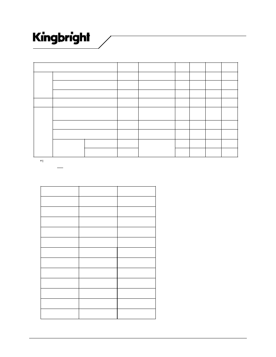
X 100%
Classification table of current transfer ratio is shown below.
CTR=
F
I
Ic
*Electro-optical Characteristics
.
o
N
l
e
d
o
M
.
o
N
l
e
d
o
M
.
o
N
l
e
d
o
M
.
o
N
l
e
d
o
M
.
o
N
l
e
d
o
M
k
r
a
m
k
n
a
R
k
r
a
m
k
n
a
R
k
r
a
m
k
n
a
R
k
r
a
m
k
n
a
R
k
r
a
m
k
n
a
R
)
%
(
R
T
C
)
%
(
R
T
C
)
%
(
R
T
C
)
%
(
R
T
C
)
%
(
R
T
C
B
-
L
7
3
8
B
K
L
0
0
1
o
t
0
5
B
-
A
7
3
8
B
K
A
0
6
1
o
t
0
8
B
-
B
7
3
8
B
K
B
0
6
2
o
t
0
3
1
B
-
C
7
3
8
B
K
C
0
0
4
o
t
0
0
2
B
-
D
7
3
8
B
K
D
0
0
6
o
t
0
0
3
B
-
B
A
7
3
8
B
K
B
r
o
A
0
6
2
o
t
0
8
B
-
C
B
7
3
8
B
K
C
r
o
B
0
0
4
o
t
0
3
1
B
-
D
C
7
3
8
B
K
D
r
o
C
0
0
6
o
t
0
0
2
B
-
C
A
7
3
8
B
K
C
r
o
B
,
A
0
0
4
o
t
0
8
B
-
D
B
7
3
8
B
K
D
r
o
C
,
B
0
0
6
o
t
0
3
1
B
-
D
A
7
3
8
B
K
D
r
o
C
,
B
,
A
0
0
6
o
t
0
8
B
-
7
3
8
B
K
k
r
a
m
o
N
r
o
D
,
C
,
B
,
A
,
L
0
0
6
o
t
0
5
r
e
t
e
m
a
r
a
P
r
e
t
e
m
a
r
a
P
r
e
t
e
m
a
r
a
P
r
e
t
e
m
a
r
a
P
r
e
t
e
m
a
r
a
P
l
o
b
m
y
S
l
o
b
m
y
S
l
o
b
m
y
S
l
o
b
m
y
S
l
o
b
m
y
S
s
n
o
it
i
d
n
o
C
s
n
o
it
i
d
n
o
C
s
n
o
it
i
d
n
o
C
s
n
o
it
i
d
n
o
C
s
n
o
it
i
d
n
o
C
.
n
i
M .
n
i
M .
n
i
M .
n
i
M .
n
i
M
.
p
y
T .
p
y
T .
p
y
T .
p
y
T .
p
y
T
.
x
a
M .
x
a
M .
x
a
M .
x
a
M .
x
a
M
ti
n
U ti
n
U ti
n
U ti
n
U ti
n
U
t
u
p
n
I
e
g
a
tl
o
v
d
r
a
w
r
o
F
V
F
I
F
A
m
0
2
=
_
_
_
2
.
1
4
.
1
V
e
g
a
tl
o
v
d
r
a
w
r
o
f
k
a
e
P
V
M
F
I
M
F
A
5
.
0
=
_
_
_
_
_
_
0
.
3
V
t
n
e
r
r
u
c
e
s
r
e
v
e
R
I
R
V
R
V
4
=
_
_
_
_
_
_
0
1
�
A
t
u
p
t
u
O
t
n
e
r
r
u
c
k
r
a
d
r
o
t
c
e
ll
o
C
I
O
E
C
V
E
C
,
V
0
2
=
I
F
A
m
0
=
_
_
_
_
_
_
0
1
7
-
A
n
r
e
f
s
n
a
r
T
-t
c
a
r
a
h
c
s
c
it
s
ir
e
1
*
o
it
a
r
r
e
f
s
n
a
rt
t
n
e
r
r
u
C
R
T
C
I
F
V
,
A
m
5
=
E
C
V
5
=
0
5
_
_
_
0
0
6
%
e
g
a
tl
o
v
n
o
it
a
r
u
t
a
s
r
e
tt
i
m
e
-
r
o
t
c
e
ll
o
C
V
(
E
C
t
a
s
)
I
F
,
A
m
0
2
=
I
C
A
m
1
=
_
_
_
1
.
0
2
.
0
8
y
c
n
e
u
q
e
r
f
ff
o
-
t
u
C
f
c
V
E
C
,
V
5
=
I
C
A
m
2
=
R
L
0
0
1
=
,
B
d
3
-
_
_
_
0
8
_
_
_
z
H
K
e
m
it
e
s
n
o
p
s
e
R
e
m
it
e
s
i
R
t
r
V
E
C
I
,
V
2
=
C
A
m
2
=
R
L
0
0
1
=
_
_
_
4
8
1
�
s
e
m
it
ll
a
F
t
f
_
_
_
3
8
1
�
s
PHOTOCOUPLER
KB837-B
SPEC NO:DSAD1555
REV NO: V.1 DATE:MAY/05/2003 PAGE: 4 OF 7
APPROVED: J.LU
CHECKED: Tracy Deng DRAWN:Y.H.LI
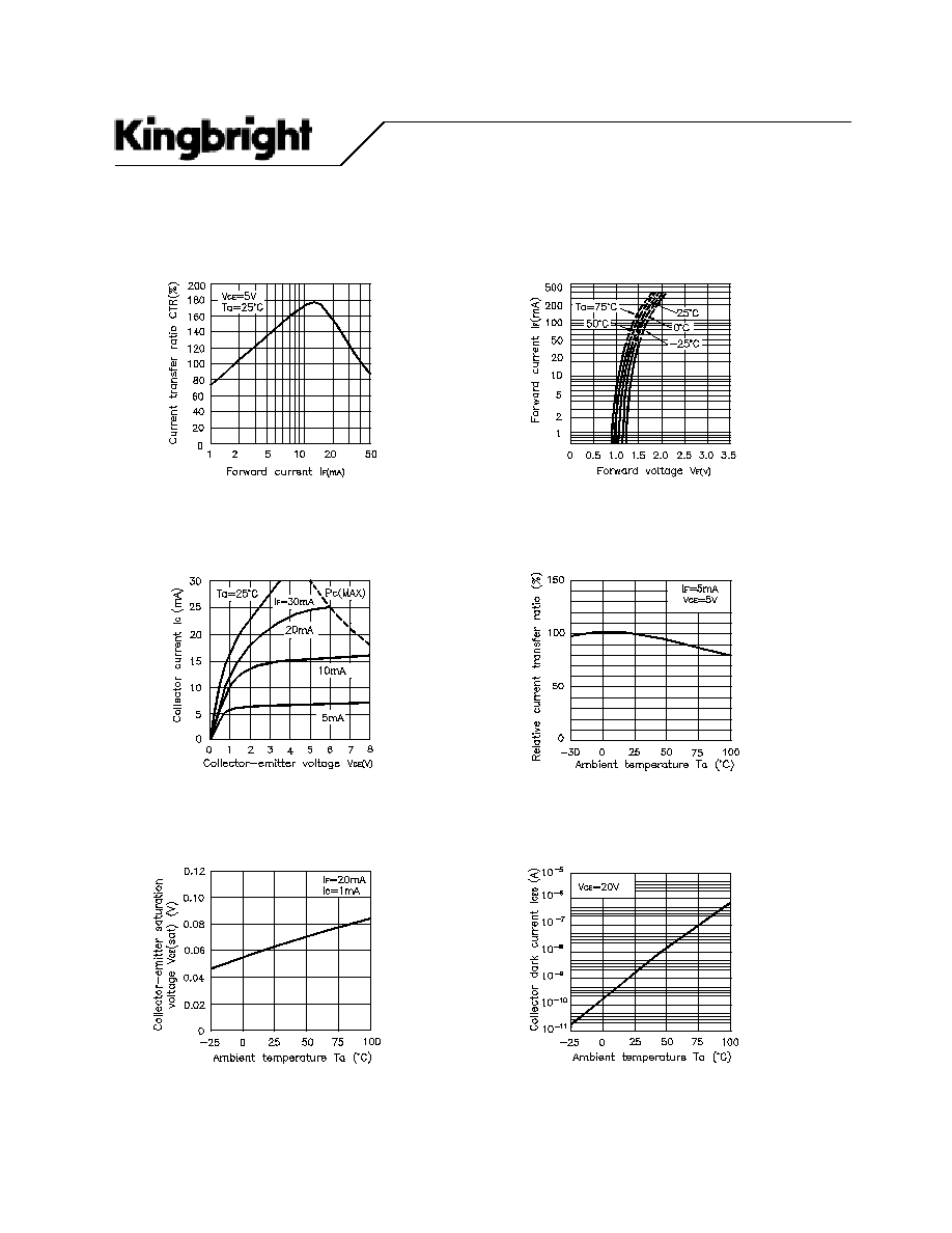
Fig. 3 Collector Current vs.
Collector-emitter Voltage
Fig. 4 Relative Current Transfer Ratio
vs. Ambient Temperature
Fig. 1 Current Transfer Ratio vs.
Forward Current
Fig. 2 Forward Current vs.
Forward voltage
Fig. 5 Collector-emitter Saturation
Voltage vs. Ambient Temperature
Fig. 6 Collector Dark Current vs.
Ambient Temperature
PHOTOCOUPLER
KB837-B
SPEC NO:DSAD1555
REV NO: V.1 DATE:MAY/05/2003 PAGE: 5 OF 7
APPROVED: J.LU
CHECKED: Tracy Deng DRAWN:Y.H.LI
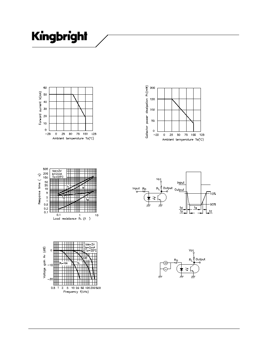
g
[
Fig. 10 Frequency Response
Test Circuit for Frequency Response
[
[
[
Fig. 9 Response Time vs.
Load Resistance
Fig. 7 Forward Current vs.
Ambient Temperature
Fig. 8 Collector Power Dissipation vs.
Ambient Temperature
Test Circuit for Response Time