 | ÐлекÑÑоннÑй компоненÑ: KB827-B | СкаÑаÑÑ:  PDF PDF  ZIP ZIP |
Äîêóìåíòàöèÿ è îïèñàíèÿ www.docs.chipfind.ru

SPEC NO: DS AD1554
REV NO: V.5 DATE: APR/05/2005 PAGE: 1 OF 8
APPROVED: J. Lu
CHECKED: Tracy Deng DRAWN: Y.W.WANG ERP:1205000015
PHOTOCOUPLER
KB827-B
GENERAL PURPOSE
HIGH ISOLATION VOLTAGE
SINGLE TRANSISTOR TYPE
PHOTOCOUPLER SERIES
FEATURES
1.Lead forming (gull wing) type, for surface mounting.
2.High isolation voltage between input and output (Viso=5000 Vrms).
3.Compact dual-in-line package
KB827-B: 2-channel type.
4.Recognized by UL and CUL, file NO.E225308.
5.Approved by VDE 0884 Teil2(NO:40006364)
(Creepage distance between input and output:7mm or more).
6.RoHS Compliant.
DESCRIPTION
1.The KB827-B (2-channel) is optically coupled isolators containing a GaAS light emitting diode
and an NPN silicon phototransistor.
2.The lead pitch is 2.54mm.
3.Solid insulation thickness between emitting diode and output phototransistor:>=0.6mm.
APPLICATIONS
1.Computer terminals.
2.Registers,copiers,automatic vending machines.
3.System appliances, measuring instruments.
4.Programmable logic controller.
5.Signal transmission between circuits of different potentials and impedances.
SPEC NO: DS AD1554
REV NO: V.5 DATE: APR/05/2005 PAGE: 2 OF 8
APPROVED: J. Lu
CHECKED: Tracy Deng DRAWN: Y.W.WANG ERP:1205000015
PHOTOCOUPLER
KB827-B
*
*
*
*
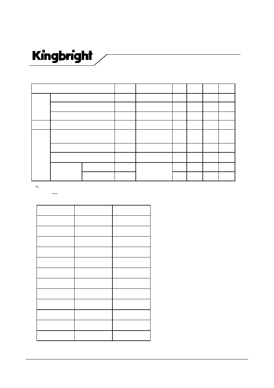
Absolute Maximum Ratings (Ta=25
°
°
°
°
C
C
C
C))))
Parameter
Symbol
Rating
Unit
Input
Forward current
I
F
50
mA
Reverse voltage
V
R
6
V
Power dissipation
P
70
mW
Output
Collector-emitter voltage
V
C E O
35
V
Emitter-collector voltage
V
E C O
6
V
Collector current
I
C
50
mA
Collector power dissipation
P
C
150
mW
Total power dissipation
Ptot
200
mW
*1
Isolation voltage
Viso
5000
Vrms
Operating temperature
Topr
-30~+100
°
C
Storage temperature
Tstg
-55~+125
°
C
*2
Soldering temperature
Tsol
260
°
C
* 1
40 t o 60% RH,A C f or 1 minut e.
* 2
For 10 s ec onds.
*
*
*
*
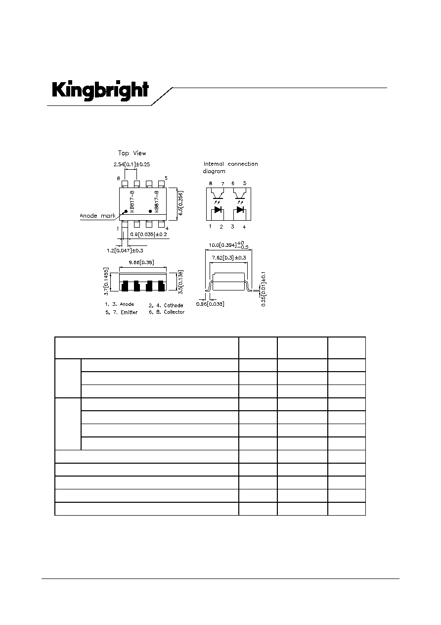
PACKAGE DIMENSIONS (UNIT:mm)
Lead Bending Type
TOLERANCE :
±
±
±
±
0.5[
±0
±0
±0
±0
.02] UNLESS OTHERWISE NOTED.
SPEC NO: DS AD1554
REV NO: V.5 DATE: APR/05/2005 PAGE: 3 OF 8
APPROVED: J. Lu
CHECKED: Tracy Deng DRAWN: Y.W.WANG ERP:1205000015
PHOTOCOUPLER
KB827-B
*
*
*
*
Electro-optical Characteristics
Parameter
Symbol
Conditions
Min.
Typ.
Max.
Unit
Input
Forward voltage
V
F
I
F
=20mA
___
1.2
1.4
V
Peak forward voltage
V
FM
I
FM
=0.5A
___
___
3.0
V
Reverse current
I
R
V
R
=4V
___
___
10
µ
A
Output
Collector dark current
I
CEO
V
CE
=20V,I
F
=0mA
___
___
10
-7
nA
Transfer
charact-
eristics
*1
Current transfer ratio
CTR
I
F
=5mA,V
CE
=5V
50
___
600
%
Collector-emitter saturation voltage
V
CE(
sat
)
I
F
=20mA, I
C
=1mA
___
0.1
0.2
C ut-o ff fre q ue nc y
f
c
V
CE
=5V, I
C
=2mA
R
L
=100
,
-3dB
___
80
___
KHz
Response time
Rise time
t
r
V
CE
=2V, I
C
=2mA
R
L
=100
___
4
18
µ
s
Fall time
t
f
___
3
18
µ
s
X 100%
Classification table of current transfer ratio is shown below.
CTR=
F
I
Ic
Model No.
Rank mark
CTR(% )
KB827L-B
L
50 to 100
KB827A-B
A
80 to 160
KB827B-B
B
130 to 260
KB827C-B
C
200 to 400
KB827D-B
D
300 to 600
KB827AB-B
A or B
80 to 260
KB827BC-B
B or C
130 to 400
KB827CD-B
C or D
200 to 600
KB827AC-B
A,B or C
80 to 400
KB827BD-B
B,C or D
130 to 600
KB827AD-B
A,B,C or D
80 to 600
KB827-B
L,A,B,C,D or No mark
50 to 600
A
SPEC NO: DS AD1554
REV NO: V.5 DATE: APR/05/2005 PAGE: 4 OF 8
APPROVED: J. Lu
CHECKED: Tracy Deng DRAWN: Y.W.WANG ERP:1205000015
PHOTOCOUPLER
KB827-B
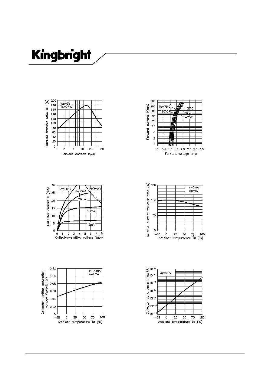
Fig. 3 Collector Current vs.
Collector-emitter Voltage
Fig. 4 Relative Current Transfer Ratio
vs. Ambient Temperature
Fig. 1 Current Transfer Ratio vs.
Forward Current
Fig. 2 Forward Current vs.
Forward voltage
Fig. 5 Collector-emitter Saturation
Voltage vs. Ambient Temperature
Fig. 6 Collector Dark Current vs.
Ambient Temperature
SPEC NO: DS AD1554
REV NO: V.5 DATE: APR/05/2005 PAGE: 5 OF 8
APPROVED: J. Lu
CHECKED: Tracy Deng DRAWN: Y.W.WANG ERP:1205000015
PHOTOCOUPLER
KB827-B
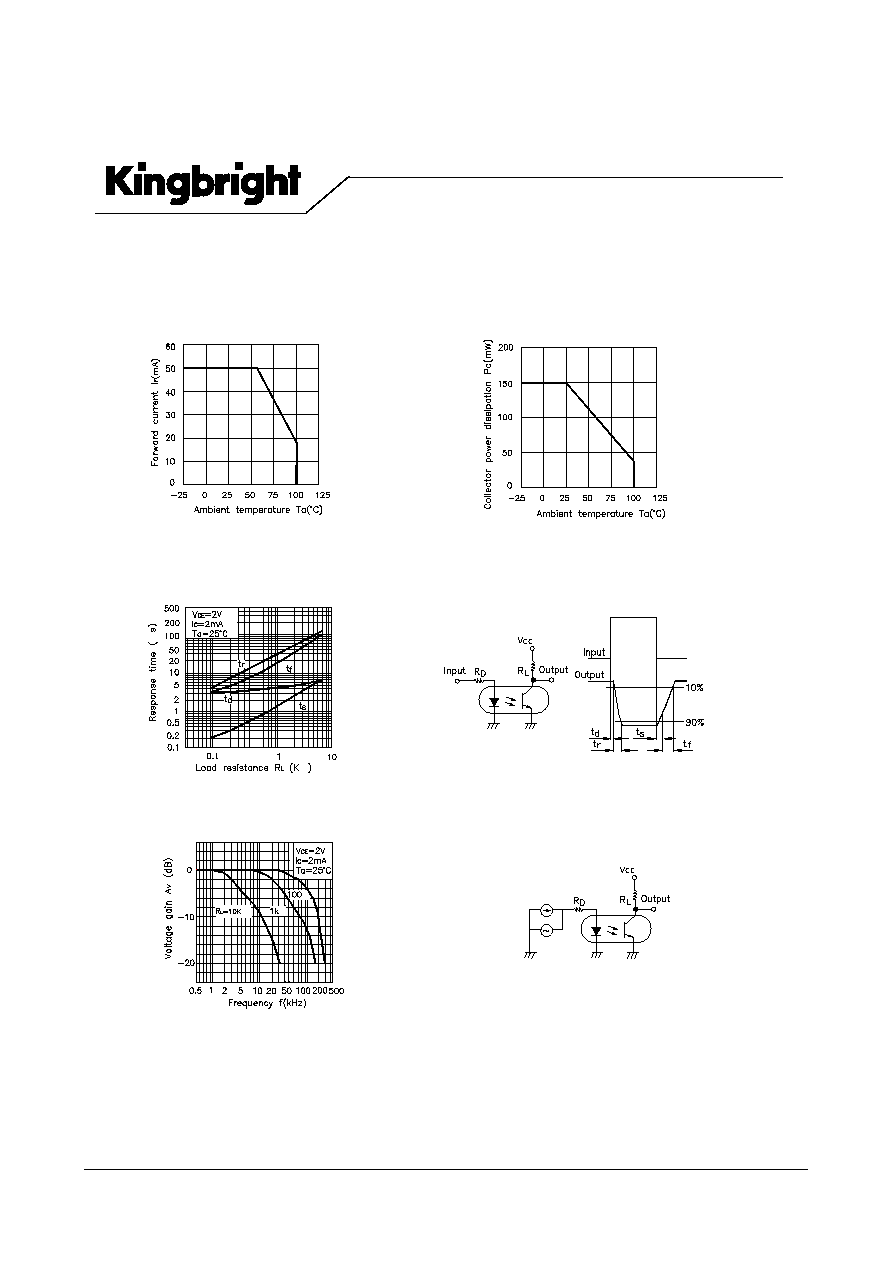
Fig. 10 Frequency Response
Test Circuit for Frequency Response
Fig. 9 Response Time vs.
Load Resistance
Fig. 7 Forward Current vs.
Ambient Temperature
Fig. 8 Collector Power Dissipation vs.
Ambient Temperature
Test Circuit for Response Time