 | ÐлекÑÑоннÑй компоненÑ: IRF7420TR | СкаÑаÑÑ:  PDF PDF  ZIP ZIP |
/home/web/doc/html/irf/174552
Parameter
Max.
Units
V
DS
Drain- Source Voltage
-20
V
I
D
@ T
A
= 25°C
Continuous Drain Current, V
GS
@ -4.5V
-11.5
I
D
@ T
A
= 70°C
Continuous Drain Current, V
GS
@ -4.5V
-9.2
A
I
DM
Pulsed Drain Current
-46
P
D
@T
A
= 25°C
Power Dissipation
2.5
P
D
@T
A
= 70°C
Power Dissipation
1.6
Linear Derating Factor
20
mW/°C
V
GS
Gate-to-Source Voltage
±8
V
T
J,
T
STG
Junction and Storage Temperature Range
-55 to +150
°C
07/11/01
www.irf.com
1
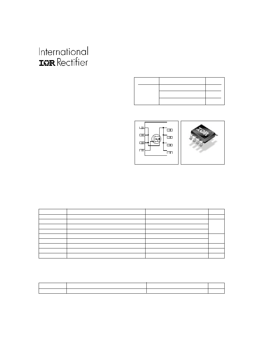
IRF7420
HEXFET
®
Power MOSFET
These P-Channel HEXFET
®
Power MOSFETs from
International Rectifier utilize advanced processing
techniques to achieve the extremely low on-resistance
per silicon area. This benefit provides the designer
with an extremely efficient device for use in battery
and load management applications..
The SO-8 has been modified through a customized
leadframe for enhanced thermal characteristics and
multiple-die capability making it ideal in a variety of
power applications. With these improvements, multiple
devices can be used in an application with dramatically
reduced board space. The package is designed for
vapor phase, infrared, or wave soldering techniques.
Description
l
Ultra Low On-Resistance
l
P-Channel MOSFET
l
Surface Mount
l
Available in Tape & Reel
PD - 94278
Parameter
Max.
Units
R
JA
Maximum Junction-to-Ambient
50
°C/W
Thermal Resistance
Absolute Maximum Ratings
W
T o p V ie w
8
1
2
3
4
5
6
7
D
D
D
G
S
A
D
S
S
SO-8
V
DSS
R
DS(on)
max
I
D
-12V
14m
@V
GS
= -4.5V
-
11.5A
17.5m
@V
GS
= -2.5V
-
9.8A
26m
@V
GS
= -1.8V
-
8.1A
IRF7420
2
www.irf.com
Parameter
Min. Typ. Max. Units
Conditions
I
S
Continuous Source Current
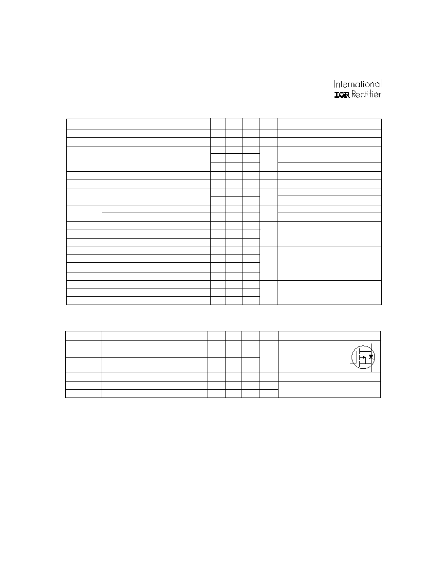
MOSFET symbol
(Body Diode)
showing the
I
SM
Pulsed Source Current
integral reverse
(Body Diode)
p-n junction diode.
V
SD
Diode Forward Voltage
-1.2
V
T
J
= 25°C, I
S
= -2.5A, V
GS
= 0V
t
rr
Reverse Recovery Time
62
93
ns
T
J
= 25°C, I
F
= -2.5A
Q
rr
Reverse Recovery Charge
61
92
µC
di/dt = -100A/µs
Source-Drain Ratings and Characteristics
A
-46
-2.5
S
D
G
Repetitive rating; pulse width limited by
max. junction temperature.
Notes:
Pulse width
400µs; duty cycle
2%.
Electrical Characteristics @ T
J
= 25°C (unless otherwise specified)
Surface mounted on 1 in square Cu board, t
10sec.
Parameter
Min. Typ. Max. Units
Conditions
V
(BR)DSS
Drain-to-Source Breakdown Voltage
-12
V
V
GS
= 0V, I
D
= -250µA
V
(BR)DSS
/
T
J
Breakdown Voltage Temp. Coefficient
0.007
V/°C
Reference to 25°C, I
D
= -1mA
14
V
GS
= -4.5V, I
D
= -11.5A
17.5
V
GS
= -2.5V, I
D
= -9.8A
26
V
GS
= -1.8V, I
D
= -8.1A
V
GS(th)
Gate Threshold Voltage
-0.4
-0.9
V
V
DS
= V
GS
, I
D
= -250µA
g
fs
Forward Transconductance
32
S
V
DS
= -10V, I
D
= -11.5A
-1.0
V
DS
= -9.6V, V
GS
= 0V
-25
V
DS
= -9.6V, V
GS
= 0V, T
J
= 70°C
Gate-to-Source Forward Leakage
-100
V
GS
= -8V
Gate-to-Source Reverse Leakage
100
V
GS
= 8V
Q
g
Total Gate Charge
38
I
D
= -11.5A
Q
gs
Gate-to-Source Charge
8.1
nC
V
DS
= -6V
Q
gd
Gate-to-Drain ("Miller") Charge
8.7
V
GS
= -4.5V
t
d(on)
Turn-On Delay Time
8.8
13
V
DD
= -6V, V
GS
= -4.5V
t
r
Rise Time
8.8
13
I
D
= -1.0A
t
d(off)
Turn-Off Delay Time
291
437
R
D
= 6
t
f
Fall Time
225
338
R
G
= 6
C
iss
Input Capacitance
3529
V
GS
= 0V
C
oss
Output Capacitance
1013
pF
V
DS
= -10V
C
rss
Reverse Transfer Capacitance
656
= 1.0MHz
I
GSS
µA
m
R
DS(on)
Static Drain-to-Source On-Resistance
I
DSS
Drain-to-Source Leakage Current
nA
ns
IRF7420
www.irf.com
3
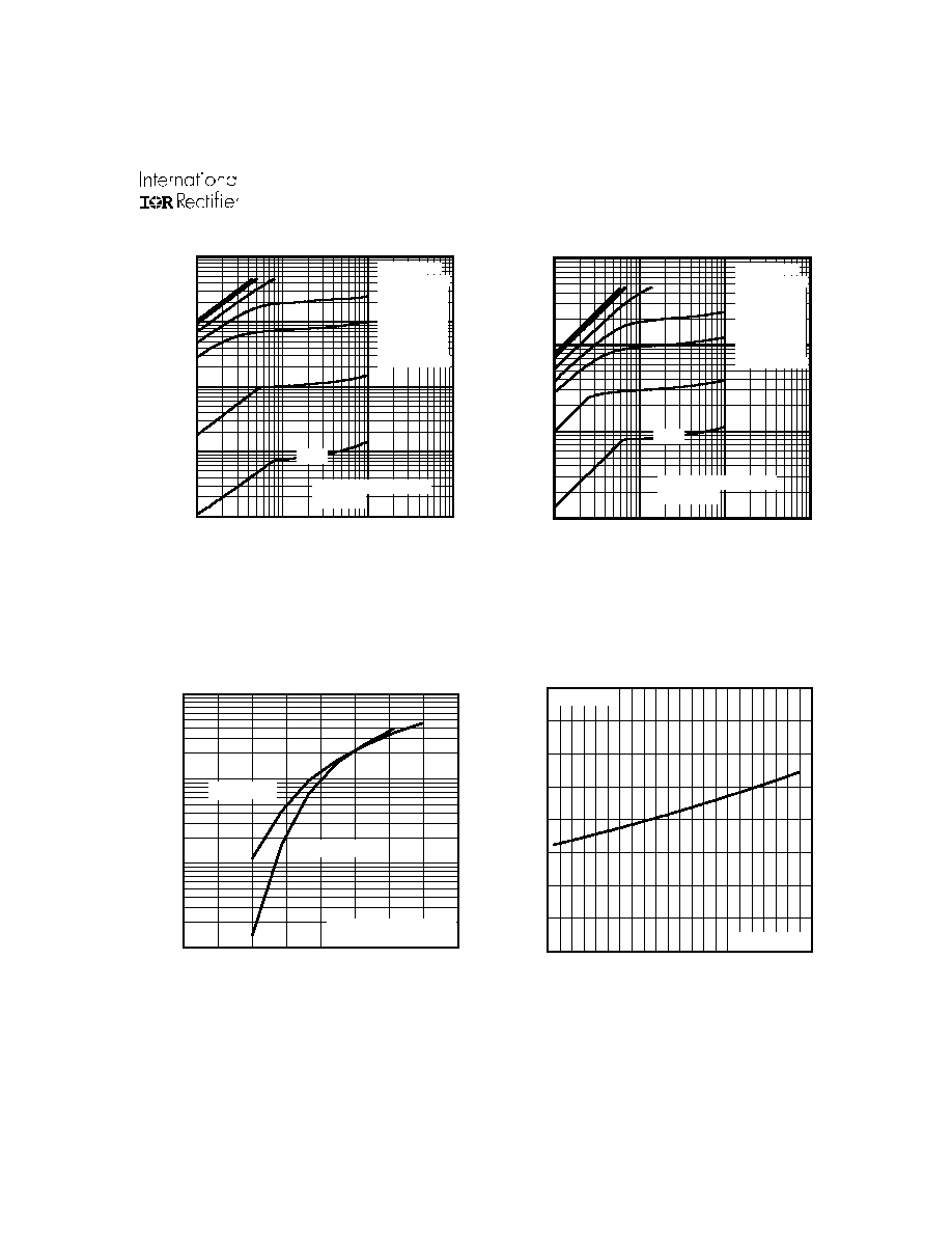
Fig 4. Normalized On-Resistance
Vs. Temperature
Fig 2. Typical Output Characteristics
Fig 1. Typical Output Characteristics
Fig 3. Typical Transfer Characteristics
0.1
1
10
100
-VDS, Drain-to-Source Voltage (V)
0.01
0.1
1
10
100
-I
D
, Drain-to-Source Current (A)
-1.0V
20µs PULSE WIDTH
Tj = 25°C
VGS
TOP -7.0V
-5.0V
-4.5V
-2.5V
-1.8V
-1.5V
-1.2V
BOTTOM -1.0V
0.1
1
10
100
-VDS, Drain-to-Source Voltage (V)
0.1
1
10
100
-I
D
, Drain-to-Source Current (A)
-1.0V
20µs PULSE WIDTH
Tj = 150°C
VGS
TOP -7.0V
-5.0V
-4.5V
-2.5V
-1.8V
-1.5V
-1.2V
BOTTOM -1.0V
-60 -40 -20
0
20
40
60
80 100 120 140 160
0.0
0.5
1.0
1.5
2.0
T , Junction Temperature ( C)
R , Drain-to-Source On Resistance
(Normalized)
J
DS(on)
°
V
=
I =
GS
D
-4.5V
-11.5A
0.1
1
10
100
0.5
1.0
1.5
2.0
2.5
V = -10V
20µs PULSE WIDTH
DS
-V , Gate-to-Source Voltage (V)
-I , Drain-to-Source Current (A)
GS
D
T = 25 C
J
°
T = 150 C
J
°
IRF7420
4
www.irf.com
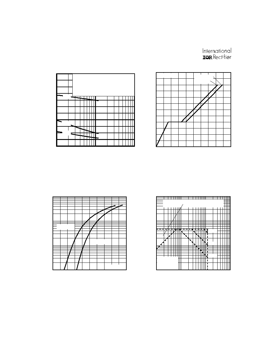
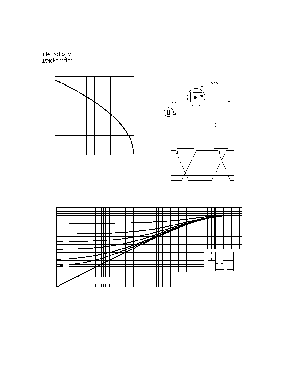
Fig 8. Maximum Safe Operating Area
Fig 6. Typical Gate Charge Vs.
Gate-to-Source Voltage
Fig 5. Typical Capacitance Vs.
Drain-to-Source Voltage
Fig 7. Typical Source-Drain Diode
Forward Voltage
0
10
20
30
40
50
0
1
2
3
4
5
6
Q , Total Gate Charge (nC)
-V , Gate-to-Source Voltage (V)
G
GS
I =
D
-11.5A
V
=-6V
DS
V
=-9.6V
DS
0.1
1
10
100
0.2
0.4
0.6
0.8
1.0
1.2
-V ,Source-to-Drain Voltage (V)
-I , Reverse Drain Current (A)
SD
SD
V = 0 V
GS
T = 25 C
J
°
T = 150 C
J
°
1
10
100
1000
0.1
1
10
100
OPERATION IN THIS AREA LIMITED
BY R
DS(on)
Single Pulse
T
T
= 150 C
= 25 C
°
°
J
C
-V , Drain-to-Source Voltage (V)
-I , Drain Current (A)
I , Drain Current (A)
DS
D
100us
1ms
10ms
1
10
100
-VDS, Drain-to-Source Voltage (V)
0
500
1000
1500
2000
2500
3000
3500
4000
4500
5000
5500
C, Capacitance(pF)
Coss
Crss
Ciss
VGS = 0V, f = 1 MHZ
Ciss = Cgs + Cgd, Cds SHORTED
Crss = Cgd
Coss = Cds + Cgd
IRF7420
www.irf.com
5
Fig 11. Maximum Effective Transient Thermal Impedance, Junction-to-Ambient
Fig 9. Maximum Drain Current Vs.
Case Temperature
0.1
1
10
100
0.00001
0.0001
0.001
0.01
0.1
1
10
100
Notes:
1. Duty factor D = t / t
2. Peak T = P
x Z
+ T
1
2
J
DM
thJA
A
P
t
t
DM
1
2
t , Rectangular Pulse Duration (sec)
Thermal Response
(Z )
1
thJA
0.01
0.02
0.05
0.10
0.20
D = 0.50
SINGLE PULSE
(THERMAL RESPONSE)
25
50
75
100
125
150
0
3
6
9
12
T , Case Temperature ( C)
-I , Drain Current (A)
°
C
D
V
DS
V
GS
Pulse Width
1
µs
Duty Factor
0.1 %
R
D
V
GS
V
DD
R
G
D.U.T.
+
-
V
DS
90%
10%
V
GS
t
d(on)
t
r
t
d(off)
t
f
Fig 10a. Switching Time Test Circuit
Fig 10b. Switching Time Waveforms