 | ÐлекÑÑоннÑй компоненÑ: 175BGQ045 | СкаÑаÑÑ:  PDF PDF  ZIP ZIP |
Äîêóìåíòàöèÿ è îïèñàíèÿ www.docs.chipfind.ru
I
F(AV)
Rectangular waveform
175
A
@ T
C
107
°C
I
DC
Maximum
248
A
V
RRM
45
V
I
FSM
@ tp = 5 µs sine
8700
A
V
F
@
175 Apk typical
0.61
V
@ T
J
150
°C
T
J
range
- 55 to 150
°C
SCHOTTKY RECTIFIER
175 Amp
1 7 5 B G Q 0 4 5
175BGQ045J
PD-20710 rev. C 11/99
www.irf.com
Characteristics
175BGQ045
Units
The NEW 175BGQ045 Schottky rectifier has been optimized for
ultra low forward voltage drop specifically for low voltage output in
high current AC/DC power supplies.
The proprietary barrier technology allows for reliable operation up
to 150°C junction temperature. Typical applications are in
switching power supplies, converters, reverse battery protection,
and redundant power subsystems.
150°C T
J
operation
High Frequency Operation
Ultra low forward voltage drop
Continuous High Current operation
Guard ring for enhanced ruggedness and long term
reliability
PowIRtab
TM
package
Major Ratings and Characteristics
Description/Features
1
Case Styles
175BGQ045
175BGQ045J
175BGQ045, 175BGQ045J
PD-20710 rev. C 11/99
www.irf.com
2
Voltage Ratings
V
FM
Forward Voltage Drop (1) (2)
0.53 0.56
V
@ 100A
0.64 0.69
V
@ 175A
0.48 0.52
V
@ 100A
0.61 0.64
V
@ 175A
I
RM
Reverse Leakage Current (1)
0.6
2
mA
T
J
= 25 °C
360
640
mA
T
J
= 125°C
1200 2000
mA
T
J
= 150 °C
V
R
= 45V
V
F(TO)
Threshold Voltage
0.352
V
T
J
=
T
J
max.
r
t
Forward Slope Resistance
1.5
m
C
T
Max. Junction Capacitance
5600
pF
V
R
= 5V
DC
, (test signal range 100Khz to 1Mhz) 25 °C
L
S
Typical Series Inductance
3.5
nH
Measured from tab to mounting plane
dv/dt Max. Voltage Rate of Change
10,000
V/ µs
(Rated V
R
)
T
J
Max. Junction Temperature Range
-55 to 150
°C
T
stg
Max. Storage Temperature Range
-55 to 150
°C
R
thJC
Max. Thermal Resistance Junction
0.25
°C/W
DC operation
to Case
R
thCS
Typical Thermal Resistance, Case to
0.20
°C/W
Mounting surface , smooth and greased
Heatsink
wt
Approximate Weight
5 (0.18)
g (oz.)
T
Mounting Torque
Min.
1.2 (10)
Max.
2.4 (20)
Case Style
PowIRtab
TM
N*m
(Ibf-in)
Thermal-Mechanical Specifications
Parameters
175BGQ
Units
Conditions
I
F(AV)
Max. Average Forward Current
175
A
50% duty cycle @ T
C
= 107°C, rectangular wave form
I
F(RMS)
RMS Forward Current
248
A
T
C
= 104°C
I
FSM
Max. Peak One Cycle Non-Repetitive
8700
5µs Sine or 3µs Rect. pulse
Surge Current
1550
10ms Sine or 6ms Rect. pulse
E
AS
Non-Repetitive Avalanche Energy
40
mJ
T
J
= 25 °C, I
AS
= 6 Amps, L = 2.0 mH
I
AR
Repetitive Avalanche Current
6
A
Current decaying linearly to zero in 1 µsec
Frequency limited by T
J
max. V
A
= 1.5 x V
R
typical
Parameters
175BGQ
Units
Conditions
Absolute Maximum Ratings
A
Following any rated
load condition and
with rated V
RRM
applied
T
J
= 25 °C
V
R
= rated V
R
Electrical Specifications
Parameters
175BGQ
Units
Conditions
Typ.
Max.
(1) Pulse Width < 300µs, Duty Cycle < 2%
(2) V
FM
= V
F(TO)
+ r
t
x I
F
Part number
175BGQ045
V
R
Max. DC Reverse Voltage (V)
V
RWM
Max. Working Peak Reverse Voltage (V)
45
T
J
= 150 °C
175BGQ045, 175BGQ045J
3
PD-20710 rev. C 11/99
www.irf.com
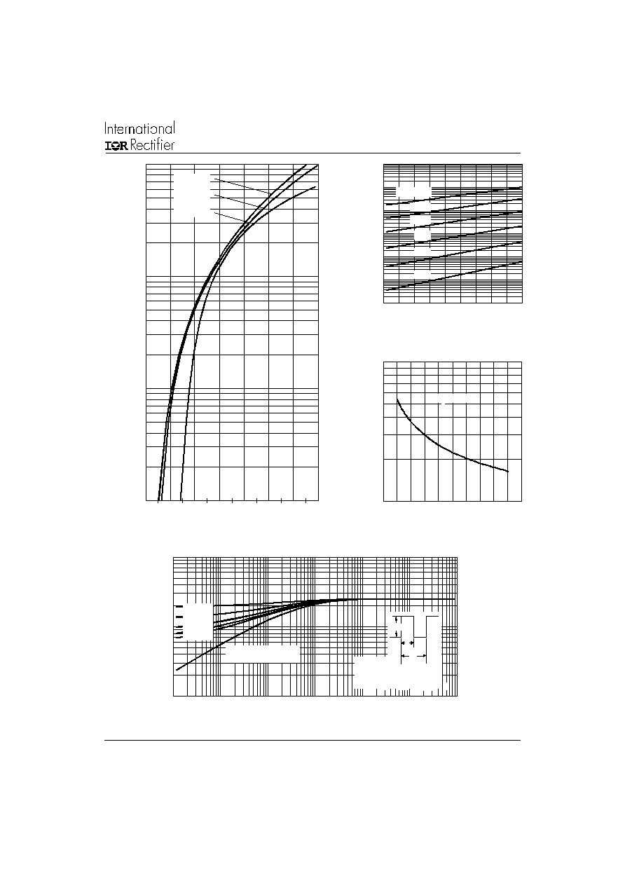
Fig. 2 - Typical Values of Reverse Current
Vs. Reverse Voltage
Fig. 3 - Typical Junction Capacitance
Vs. Reverse Voltage
Fig. 4 - Maximum Thermal Impedance Z
thJC
Characteristics
Fig. 1 - Maximum Forward Voltage Drop Characteristics
1
1 0
10 0
1 00 0
0
0 .2
0 .4
0. 6
0. 8
1
1 .2
1 .4
F
FM
T = 15 0°C
T = 12 5°C
T = 2 5°C
J
J
J
Forw ard Voltage Drop - V (V)
I
n
s
t
an
t
a
n
e
o
u
s
F
o
r
w
ar
d
C
u
r
r
e
n
t
-
I
(
A
)
0 .0 1
0 .1
1
1 0
1 0 0
1 0 0 0
1 0 0 0 0
0
5
1 0
1 5
2 0
2 5
3 0
3 5
4 0
4 5
R
R
1 2 5 °C
1 0 0 °C
7 5 °C
5 0 °C
2 5 °C
R
e
v
e
rs
e
C
u
rre
n
t
-
I
(
m
A
)
R e v e rse V o lt a g e - V ( V )
T = 1 5 0 °C
J
1 0 0 0
1 0 0 0 0
0
1 0
2 0
3 0
4 0
5 0
R
T
J
u
n
c
ti
o
n
C
a
p
a
c
i
ta
n
c
e
-
C
(
p
F
)
R e v e rse V o lt a g e - V ( V )
T = 2 5 °C
J
0 .0 1
0 .1
1
0. 00 0 01
0. 00 0 1
0 .0 01
0 .0 1
0.1
1
1 0
th
J
C
t , R ec ta n gu lar Pu lse D u ra tio n (S ec on d s)
Sin gle P u ls e
(Ther m a l R esista n c e)
1
T
h
e
r
m
a
l
I
m
p
e
d
a
n
c
e
Z
(
°
C
/
W
)
Notes:
1 . Duty fac tor D = t / t
2 . Peak T = P x Z + T
1
2
J
th J C
C
D M
D = 0 .7 5
D = 0 .5 0
D = 0 .3 3
D = 0 .2 5
D = 0 .2 0
2
t
1
t
P
DM
175BGQ045, 175BGQ045J
PD-20710 rev. C 11/99
www.irf.com
4
Fig. 8 - Unclamped Inductive Test Circuit
Fig. 5 - Maximum Allowable Case Temperature
Vs. Average Forward Current
Fig. 6 - Forward Power Loss Characteristics
Fig. 7 - Maximum Non-Repetitive Surge Current
(3) Formula used: T
C
= T
J
- (Pd + Pd
REV
) x R
thJC
;
Pd = Forward Power Loss = I
F(AV)
x V
FM
@ (I
F(AV)
/
D) (see Fig. 6);
Pd
REV
= Inverse Power Loss = V
R1
x I
R
(1 - D); I
R
@ V
R1
= 80% rated V
R
FR E E - W H E E L
D IO D E
40 HFL4 0 S02
C U R R E N T
M O N IT O R
H IG H - SP E E D
SW IT C H
IRFP4 60
L
D U T
Rg = 25 ohm
V d = 2 5 V o lt
+
5 0
6 0
7 0
8 0
9 0
1 0 0
1 1 0
1 2 0
1 3 0
1 4 0
1 5 0
0
5 0
1 0 0
1 5 0
2 0 0
2 5 0
3 0 0
D C
A
l
l
o
w
a
b
l
e
C
a
s
e
T
e
m
p
er
a
t
u
r
e
-
(
°
C
)
F (A V)
A v e ra g e Fo rw a rd C u rr e n t - I ( A )
s e e no te ( 3 )
Sq u a re wa v e (D = 0.5 0 )
80 % Ra ted V a p p lie d
R
0
2 5
5 0
7 5
1 0 0
1 2 5
1 5 0
1 7 5
2 0 0
0
5 0
1 0 0
1 5 0
2 0 0
2 5 0
D C
A
v
e
r
a
g
e
P
o
w
e
r
L
o
ss -
(
W
a
t
t
s
)
F (A V)
R M S L im it
D = 0 .2 0
D = 0 .2 5
D = 0 .3 3
D = 0 .5 0
D = 0 .7 5
A v e ra g e Fo rw a rd C u rre n t - I ( A )
1 0 00
1 0 0 00
10
10 0
1 00 0
10 0 00
FS
M
N
o
n
-
R
e
p
e
t
i
t
i
v
e
S
u
r
g
e
C
u
r
r
e
n
t
-
I
(
A
)
p
A t A n y R a t e d L o a d C o n d it io n
A n d W it h R a te d V A p p lie d
F o llo w in g S u rg e
RRM
Sq u a r e W a v e Pu lse D u ra t io n - t ( m ic ro se c )
175BGQ045, 175BGQ045J
5
PD-20710 rev. C 11/99
www.irf.com
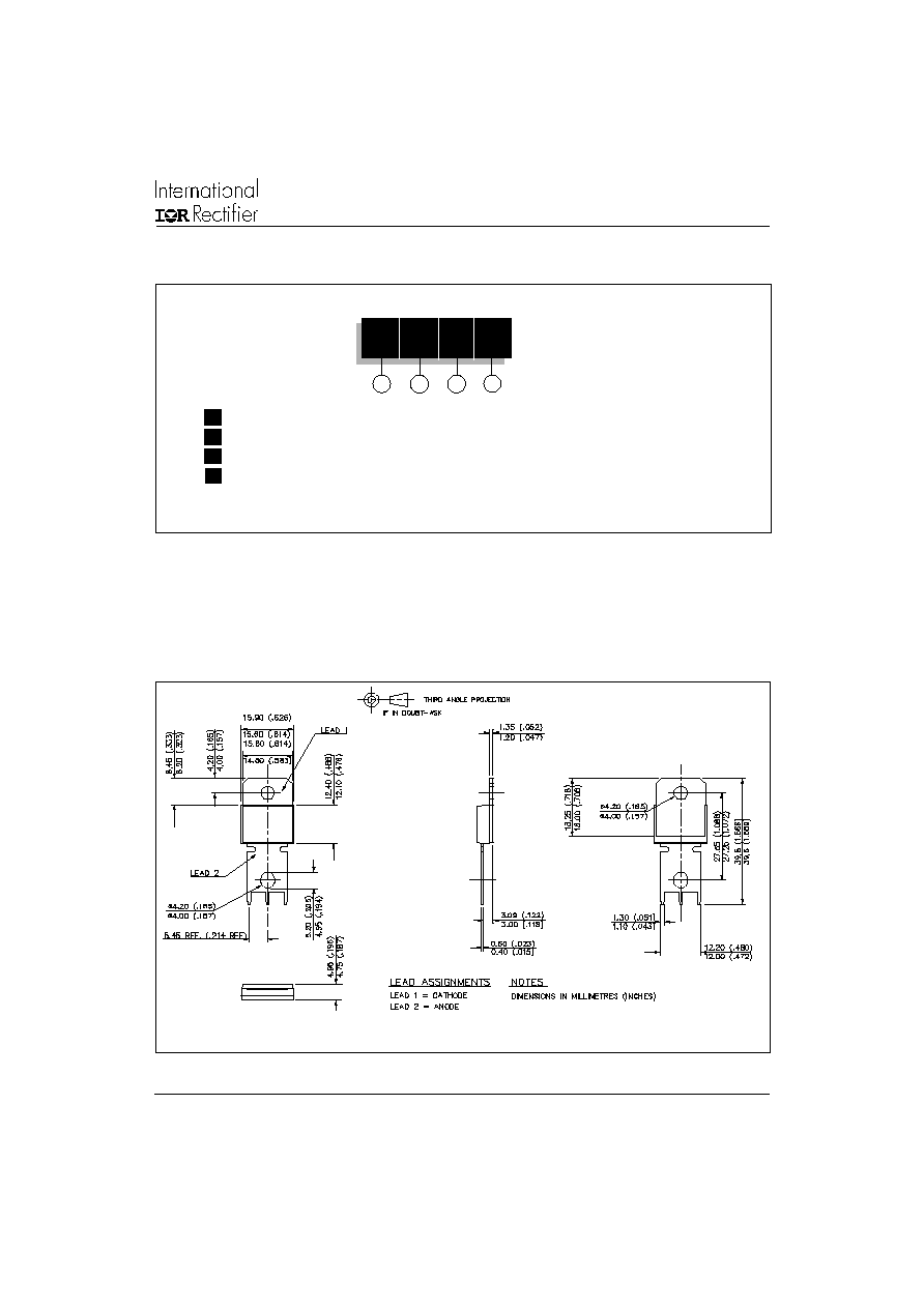
Outline Table
Case Style
PowIRtab
TM
Dimensions in millimeters and (inches)
Ordering Information Table
Device Code
1
2
4
3
1
-
Current Rating
2
-
Essential Part Number
3
-
Voltage code: Code = V
RRM
4
-
none = PowIRtab
TM
standard
6
J
= Short Lead Version
175 BGQ 045
J