ICS9161A
Integrated
Circuit
Systems, Inc.
General Description
Features
ICS9161A
9161
0210H--06/05/03
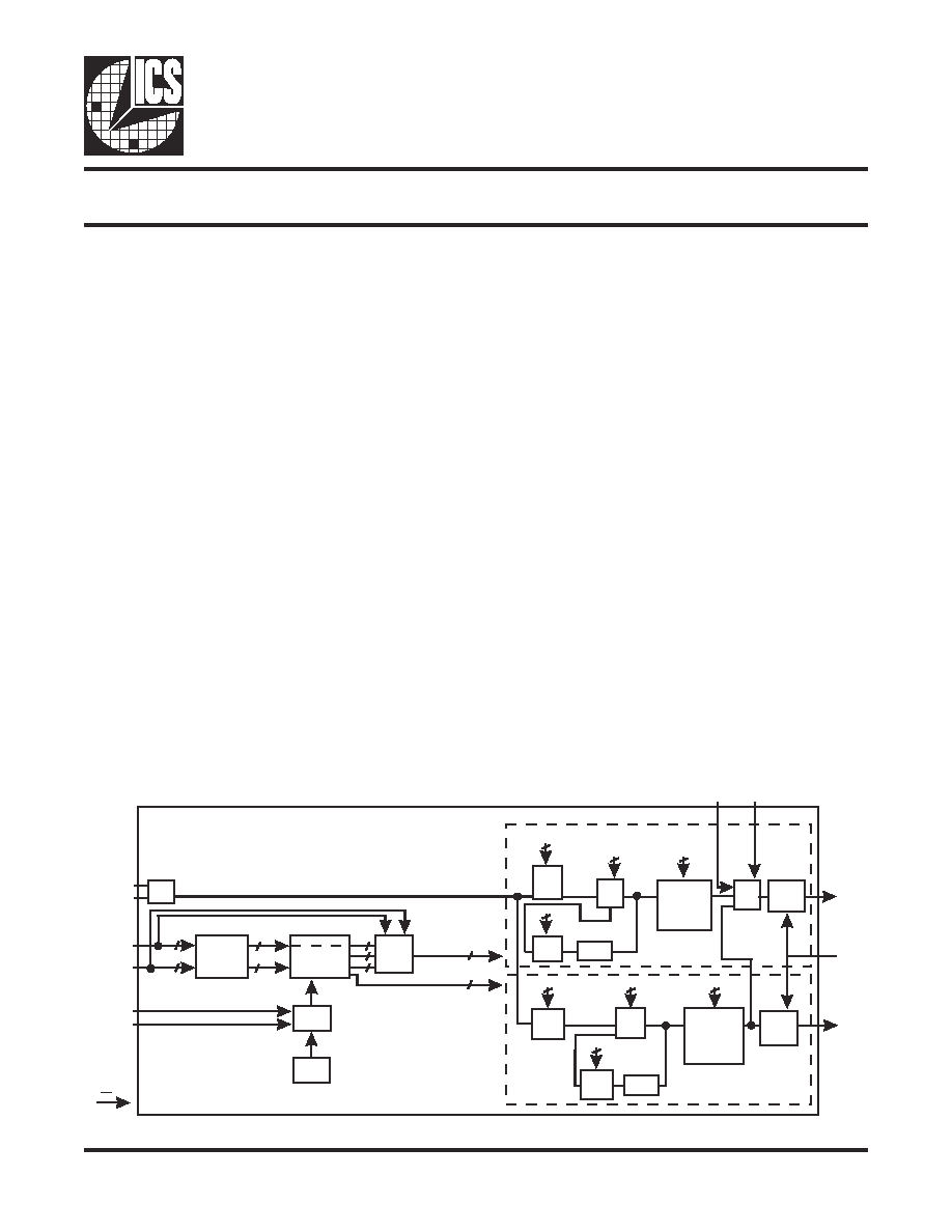
Block Diagram
Dual Programmable Graphics Frequency Generator
The ICS9161A is a fully programmable graphics clock
generator. It can generate user-specified clock
frequencies using an externally generated input
reference or a single crystal. The output frequency is
programmed by entering a 24-bit digital word through
the serial port. Two fully user-programmable phase-
locked loops are offered in a single package. One PLL
is designed to drive the memory clock, while the
second drives the video clock. The outputs may be
changed on-the-fly to any desired frequency between
390 kHz and 120 MHz. The ICS9161A is ideally suited
for any design where multiple or varying frequencies
are required.
This part is ideal for graphics applications. It generates
low jitter, high speed pixel clocks. It can be used to replace
multiple, expensive high speed crystal oscillators. The
flexibility of the device allows it to generate non-standard
graphics clocks.
The ICS9161A is also ideal in disk drives. It can generate
zone clocks for constant density recording schemes. The low
profile, 16-pin SOIC or PDIP package and low jitter outputs
are especially attractive in board space critical disk drives.
The leader in the area of multiple output clocks on a single
chip, ICS has been shipping graphics frequency generators
since October, 1990, and is constantly improving the
phase-locked loop. The ICS9161A incorporates a patented
fourth generation PLL that offers the best jitter performance
available.
�
Pin-for-pin and function compatible with ICD2061A
�
Dual programmable graphics clock generator
�
Memory and video clocks are individually
programmable on-the-fly
�
Ideal for designs where multiple or varying
frequencies are required
�
Increased frequency resolution from optional pre-
divide by 2 on the M counter
�
Output enable feature available for tristating outputs
�
Independent clock outputs range from 390 kHz to
120 MHz for VDD >4.75V
�
Power-down capabilities
�
Low power, high speed 0.8� CMOS technology
�
Glitch-free transitions
�
Available in 16-pin, 300-mil SOIC or PDIP package
EXTCLK
EXTSEL
VCO OUTPUT
DIVIDER
R=1,2,4,8,16
32,64,128
VCO
CMOS
OUTPUT
DRIVER
MCLK
OE
VCO
DIVIDE
(N�)
VCO OUTPUT
DIVIDER
R=1,2,4,8,16
32,64,128
VCO
REF
DIVIDE
(M�)
MUX
CMOS
OUTPUT
DRIVER
VCLK
D14-D20
7
D0-D3
4
D11-D13
3
REF
f
D14-D20
7
D4-D10
7
D0-D3
4
D11-D13
3
24
24
MCLK
(D0-D20)
21
21
VCLK
(D0-D20)
21
21
21
REGISTERS
3
ADDRESS
INIT
ROM
POR
INIT1
INIT2
SEL0-CLK
SEL1-DATA
DECODE
LOGIC
21
DATA
CONTROL REG
XTAL
OSC
X1
X2
PD
3-TO-1
MUX
Pscale
P= 2 or 4
REF
DIVIDE
(M�)
D4-D10
7
VCO
DIVIDE
(N�)
Pscale
P= 2
2
ICS9161A
0210H--06/05/03
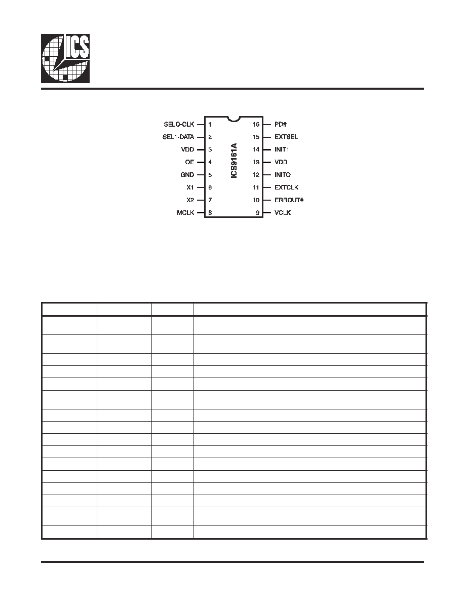
Pin Descriptions
Pin Configuration
R
E
B
M
U
N
N
I
P
E
M
A
N
N
I
P
E
P
Y
T
N
O
I
T
P
I
R
C
S
E
D
1
K
L
C
-
0
L
E
S
N
I
g
n
i
t
a
r
e
p
o
n
i
n
i
p
t
c
e
l
e
s
k
c
o
l
C
.
e
d
o
m
g
n
i
m
m
a
r
g
o
r
p
l
a
i
r
e
s
n
i
t
u
p
n
i
k
c
o
l
C
.
D
N
G
o
t
n
w
o
d
-
ll
u
p
l
a
n
r
e
t
n
i
s
a
H
.
e
d
o
m
2
A
T
A
D
-
1
L
E
S
N
I
g
n
i
t
a
r
e
p
o
n
i
n
i
p
t
c
e
l
e
s
k
c
o
l
C
.
e
d
o
m
g
n
i
m
m
a
r
g
o
r
p
l
a
i
r
e
s
n
i
t
u
p
n
i
a
t
a
D
.
D
N
G
o
t
n
w
o
d
-
ll
u
p
l
a
n
r
e
t
n
i
s
a
H
.
e
d
o
m
3
D
D
V
A
R
W
P
.
r
e
w
o
P
4
E
O
N
I
.
D
D
V
o
t
p
u
-
ll
u
p
l
a
n
r
e
t
n
i
s
a
H
.
w
o
l
n
e
h
w
s
t
u
p
t
u
o
s
e
t
a
t
s
i
r
T
5
D
N
G
R
W
P
.
d
n
u
o
r
G
6
1
X
N
I
k
c
a
b
d
e
e
f
d
n
a
e
c
n
a
t
i
c
a
p
a
c
d
a
o
l
L
A
T
X
s
e
d
u
l
c
n
i
t
u
p
n
i
s
i
h
T
.
t
u
p
n
i
l
a
t
s
y
r
C
.
l
a
t
s
y
r
c
e
h
t
r
o
f
s
a
i
b
7
2
X
T
U
O
.
e
c
n
a
t
i
c
a
p
a
c
d
a
o
l
L
A
T
X
l
a
n
r
e
t
n
i
s
e
d
u
l
c
n
i
h
c
i
h
w
t
u
p
t
u
o
l
a
t
s
y
r
C
8
K
L
C
M
T
U
O
.
t
u
p
t
u
o
k
c
o
l
c
y
r
o
m
e
M
9
K
L
C
V
T
U
O
.
t
u
p
t
u
o
k
c
o
l
c
o
e
d
i
V
0
1
#
T
U
O
R
R
E
T
U
O
.
d
r
o
w
d
e
m
m
a
r
g
o
r
p
y
ll
a
i
r
e
s
e
h
t
n
i
r
o
r
r
e
n
a
s
l
a
n
g
i
s
w
o
l
t
u
p
t
u
O
1
1
K
L
C
T
X
E
N
I
.
D
D
V
o
t
p
u
-
ll
u
p
l
a
n
r
e
t
n
i
s
a
H
.
t
u
p
n
i
k
c
o
l
c
l
a
n
r
e
t
x
E
2
1
0
T
I
N
I
N
I
.
D
N
G
o
t
n
w
o
d
-
ll
u
p
l
a
n
r
e
t
n
i
s
a
H
.
B
S
L
,
s
n
o
i
t
i
d
n
o
c
p
u
-
r
e
w
o
p
l
a
i
t
i
n
i
s
t
c
e
l
e
S
3
1
D
D
V
R
W
P
.
r
e
w
o
P
4
1
1
T
I
N
I
N
I
.
D
N
G
o
t
n
w
o
d
-
ll
u
p
l
a
n
r
e
t
n
i
s
a
H
.
B
S
M
,
s
n
o
i
t
i
d
n
o
c
p
u
-
r
e
w
o
p
l
a
i
t
i
n
i
s
t
c
e
l
e
S
5
1
L
E
S
T
X
E
N
I
-
ll
u
p
l
a
n
r
e
t
n
i
s
a
H
.
t
u
p
t
u
o
K
L
C
V
s
a
)
K
L
C
T
X
E
(
t
u
p
n
i
k
c
o
l
c
l
a
n
r
e
t
x
e
s
t
c
e
l
e
S
.
D
D
V
o
t
p
u
6
1
#
D
P
N
I
.
D
D
V
o
t
p
u
-
ll
u
p
l
a
n
r
e
t
n
i
s
a
H
.
w
o
l
e
v
i
t
c
a
,
n
i
p
n
w
o
d
-
r
e
w
o
P
16-Pin 300- mil SOIC or PDIP
3
ICS9161A
0210H--06/05/03
Register Definitions
The register file consists of the following six registers:
Register Addressing
As seen in the VCLK Selection table, OE acts to tristate
the output. The PD# pin forces the VCLK signal high while
powering down the part. The EXTCLK pin will only be
multiplexed in when EXTSEL and SEL0 are logic 0 and
SEL1 is a logic 1.
The memory clock outputs are controlled by PD# and
OE as follows:
The Clock Select pins SEL0 and SEL1 have two purposes.
In serial programming mode, these pins act as the clock
and data pins. New data bits come in on SEL1 and these
bits are clocked in by a signal on SEL0. While these pins
are acquiring new information, the VCLK signal remains
unchanged. When SEL0 and SEL1 are acting as register
selects, a time-out interval is required to determine whether
the user is selecting a new register or wants to program the
part. During this initial time-out, the VCLK signal remains
at its previous frequency. At the end of this time-out
interval, a new register is selected. A second time-out
interval is required to allow the VCO to settle to its new
value. During this period of time, typically 5ms, the input
reference signal is multiplexed to the VCLK signal.
When MCLK or the active VCLK register is being re-
programmed, then the reference signal is multiplexed
glitch-free to the output during the first time-out interval. A
second time-Register out interval is also required to allow
the VCO to settle. During this period, the reference signal
is multiplexed to the appropriate output signal.
The ICS9161A places the three video clock registers and
the memory clock register in a known state upon power-
up. The registers are initialized based on the state of the
INIT1 and INIT0 pins at application of power to the device.
The INIT pins must ramp up with VDD if a logical 1 on either
pin is required. These input pins are internally pulled down
and will default to a logical 0 if left unconnected.
The registers are initialized as follows:
Register Initialization
Register Selection
When the ICS9161A is operating, the video clock output
is controlled with a combination of the SEL0, SEL1, PD#
and OE pins. The video clock is also multiplexed to an
external clock (EXTCLK) which can be selected with the
EXTSEL pin. The VCLK Selection Table shows how VCLK
is selected.
VCLK Selection
1
T
I
N
I
0
T
I
N
I
G
E
R
M
0
G
E
R
1
G
E
R
2
G
E
R
0
0
1
1
0
1
0
1
0
0
5
.
2
3
0
0
0
.
0
4
0
5
3
.
0
5
4
4
6
.
6
5
5
7
1
.
5
2
5
7
1
.
5
2
0
0
0
.
0
4
0
0
0
.
0
4
2
2
3
.
8
2
2
2
3
.
8
2
2
2
3
.
8
2
0
5
3
.
0
5
2
2
3
.
8
2
2
2
3
.
8
2
2
2
3
.
8
2
0
5
3
.
0
5
E
O
#
D
P
L
E
S
T
X
E
1
L
E
S
0
L
E
S
K
L
C
V
0
1
1
1
1
1
1
x
0
1
1
1
1
1
x
x
x
x
0
1
x
x
x
0
0
1
1
1
x
x
0
1
0
x
1
e
t
a
t
s
i
r
T
h
g
i
H
d
e
c
r
o
F
0
G
E
R
1
G
E
R
K
L
C
T
X
E
2
G
E
R
2
G
E
R
E
O
#
D
P
K
L
C
M
0
1
1
x
1
0
e
t
a
t
s
i
r
T
G
E
R
M
N
W
D
R
W
P
MCLK Selection
s
s
e
r
d
d
A
)
0
A
-
2
A
(
r
e
t
s
i
g
e
R
n
o
i
t
i
n
i
f
e
D
0
0
0
1
0
0
0
1
0
1
1
0
0
0
1
0
1
1
0
G
E
R
1
G
E
R
2
G
E
R
G
E
R
M
N
W
D
R
W
P
G
E
R
L
T
N
C
1
r
e
t
s
i
g
e
R
k
c
o
l
C
o
e
d
i
V
2
r
e
t
s
i
g
e
R
k
c
o
l
C
o
e
d
i
V
3
r
e
t
s
i
g
e
R
k
c
o
l
C
o
e
d
i
V
r
e
t
s
i
g
e
R
y
r
o
m
e
M
e
d
o
m
n
w
o
d
-
r
e
w
o
P
r
o
f
r
o
s
i
v
i
D
r
e
t
s
i
g
e
R
l
o
r
t
n
o
C
4
ICS9161A
0210H--06/05/03
Control Register Definitions
The control register allows the user to adjust various internal options. The register is defined as follows:
t
i
B
e
m
a
N
t
i
B
e
u
l
a
V
t
l
u
a
f
e
D
n
o
i
t
p
i
r
c
s
e
D
1
2
5
C
0
.
t
n
e
m
e
l
p
m
i
ll
i
w
n
i
p
#
D
P
e
h
t
e
d
o
m
n
w
o
d
-
r
e
w
o
p
h
c
i
h
w
s
e
n
i
m
r
e
t
e
d
t
i
b
s
i
h
T
f
o
n
o
i
t
c
n
u
f
a
e
b
o
t
s
l
a
n
g
i
s
K
L
C
M
e
h
t
s
e
c
r
o
f
,
0
=
5
C
,
1
e
d
o
m
n
w
o
d
-
r
e
w
o
P
l
a
t
s
y
r
c
e
h
t
f
f
o
s
n
r
u
t
,
1
=
5
C
,
2
e
d
o
m
n
w
o
d
-
r
e
w
o
P
.
r
e
t
s
i
g
e
r
n
w
o
d
-
r
e
w
o
p
e
h
t
.
s
t
u
p
t
u
o
ll
a
s
e
l
b
a
s
i
d
d
n
a
0
2
4
C
0
y
c
n
e
u
q
e
r
f
g
n
i
r
u
d
K
L
C
V
o
t
d
e
x
e
l
p
i
t
l
u
m
s
i
k
c
o
l
c
h
c
i
h
w
s
e
n
i
m
r
e
t
e
d
t
i
b
s
i
h
T
.
t
u
p
t
u
o
K
L
C
V
e
h
t
o
t
y
c
n
e
u
q
e
r
f
e
c
n
e
r
e
f
e
r
e
h
t
s
e
x
e
l
p
i
t
l
u
m
0
=
4
C
.
s
e
g
n
a
h
c
e
h
t
e
r
e
h
w
s
n
o
i
t
a
c
il
p
p
a
r
o
f
t
u
p
t
u
o
K
L
C
V
e
h
t
o
t
K
L
C
M
s
e
x
e
l
p
i
t
l
u
m
1
=
4
C
f
s
a
w
o
l
s
s
a
n
u
r
t
o
n
n
a
c
r
e
ll
o
r
t
n
o
c
s
c
i
h
p
a
r
g
.
F
E
R
9
1
3
C
0
l
a
v
r
e
t
n
i
t
u
o
-
e
m
i
t
e
h
T
.
l
a
v
r
e
t
n
i
t
u
o
-
e
m
i
t
e
h
t
f
o
h
t
g
n
e
l
e
h
t
s
e
n
i
m
r
e
t
e
d
t
i
b
s
i
h
T
n
i
a
t
r
e
c
o
t
d
e
m
m
a
r
g
o
r
p
s
i
O
C
V
s
i
h
t
f
I
.
O
C
V
K
L
C
M
e
h
t
m
o
r
f
d
e
v
i
r
e
d
s
i
.
t
u
o
-
e
m
i
t
l
a
m
r
o
n
,
0
=
3
C
.
t
r
o
h
s
o
o
t
e
b
y
a
m
l
a
v
r
e
t
n
i
t
u
o
-
e
m
i
t
e
h
t
,
s
e
m
e
r
t
x
e
.
l
a
v
r
e
t
n
i
t
u
o
-
e
m
i
t
d
e
l
b
u
o
d
,
1
=
3
C
8
1
2
C
0
.
0
o
t
t
e
s
e
b
t
s
u
m
,
d
e
v
r
e
s
e
R
7
1
1
C
1
h
g
i
h
t
u
p
t
u
o
n
i
e
s
a
e
r
c
e
d
s
n
1
a
s
e
s
u
a
c
0
=
1
C
.
e
l
c
y
c
y
t
u
d
e
h
t
s
t
s
u
j
d
a
t
i
b
s
i
h
T
e
h
t
,
h
g
i
h
s
i
e
c
n
a
t
i
c
a
p
a
c
d
a
o
l
e
h
t
f
I
.
t
n
e
m
t
s
u
j
d
a
o
n
s
e
s
u
a
c
1
=
1
C
.
e
m
i
t
.
%
0
5
o
t
r
e
s
o
l
c
e
l
c
y
c
y
t
u
d
e
h
t
g
n
i
r
b
n
a
c
t
n
e
m
t
s
u
j
d
a
6
1
0
C
0
.
0
o
t
t
e
s
e
b
t
s
u
m
,
d
e
v
r
e
s
e
R
5
1
2
S
N
0
s
e
l
a
c
s
e
r
p
1
=
2
S
N
.
2
y
b
r
e
t
n
u
o
c
N
e
h
t
s
e
l
a
c
s
e
r
p
0
=
2
S
N
.
2
r
e
t
s
i
g
e
r
n
o
s
t
c
A
.
4
o
t
e
u
l
a
v
r
e
t
n
u
o
c
P
e
h
t
4
1
1
S
N
0
s
e
l
a
c
s
e
r
p
1
=
1
S
N
.
2
y
b
r
e
t
n
u
o
c
N
e
h
t
s
e
l
a
c
s
e
r
p
0
=
1
S
N
.
1
r
e
t
s
i
g
e
r
n
o
s
t
c
A
.
4
o
t
e
u
l
a
v
r
e
t
n
u
o
c
P
e
h
t
3
1
0
S
N
0
s
e
l
a
c
s
e
r
p
1
=
0
S
N
.
2
y
b
r
e
t
n
u
o
c
N
e
h
t
s
e
l
a
c
s
e
r
p
0
=
1
S
N
.
0
r
e
t
s
i
g
e
r
n
o
s
t
c
A
.
4
o
t
e
u
l
a
v
r
e
t
n
u
o
c
P
e
h
t
5
ICS9161A
0210H--06/05/03
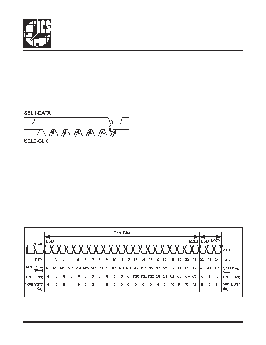
Serial Programming Architecture
The pins SEL0 and SEL1 perform the dual functions of
select-ing registers and serial programming. In serial
programming mode, SEL0 acts as a clock pin while SEL1
acts as the data pin. The ICS9161A-01 may not be serially
programmed when in power-down mode.
In order to program a particular register, an unlocking
sequence must occur. The unlocking sequence is detailed
in the following timing diagram:
Serial Data Register
The serial data is clocked into the serial data register in the
order described in Figure 1 below (Serial Data Timing).
The serial data is sent as follows: An individual data bit is
sampled on the rising edge of CLK. The complement of the
data bit must be sampled on the previous falling edge of
CLK. The setup and hold time requirements must be met
on both CLK edges. For specifics on timing, see the timing
diagrams on pages 10, 11 and 12.
The bits are shifted in this order: a start bit, 21 data bits,
3 address bits (which designate the desired register), and
a stop bit. A total of 24 bits must always be loaded into the
serial data register or an error is issued. Following the entry
of the last data bit, a stop bit or load command is issued
by bringing DATA high and toggling CLK high-to-low and
low-to-high. The unlocking mechanism then resets itself
following the load. Only after a time-out period are the
SEL0 and SEL1 pins allowed to return to a register
selection function.
Since the VCLK registers are selected by the SEL0 and
SEL1 pins, and since any change in their state may affect
the output frequency, new data input on the selection bits
is only permitted to pass through the decode logic after the
watchdog timer has timed out. This delay of SEL0 or SEL1
data permits a serial program cycle to occur without
affecting the current register selection.
The unlock sequence consists of at least five low-to-high
transitions of CLK while data is high, followed immediately
by a single low-to-high transition while data is low. Following
this unlock sequence, data can be loaded into the serial
data register. This programming must include the start bit,
shown in Figure 1.
Following any transition of CLK or DATA, the watchdog
timer is reset and begins counting. The watchdog timer
ensures that successive rising edges of CLK and DATA do
not violate the time-out specification of 2ms. If a time-out
occurs, the lock mechanism is reset and the data in the
serial data register is ignored.
Figure 1: Serial Data Timing