Integrated
Circuit
Systems, Inc.
General Description
Features
ICS9147- 01
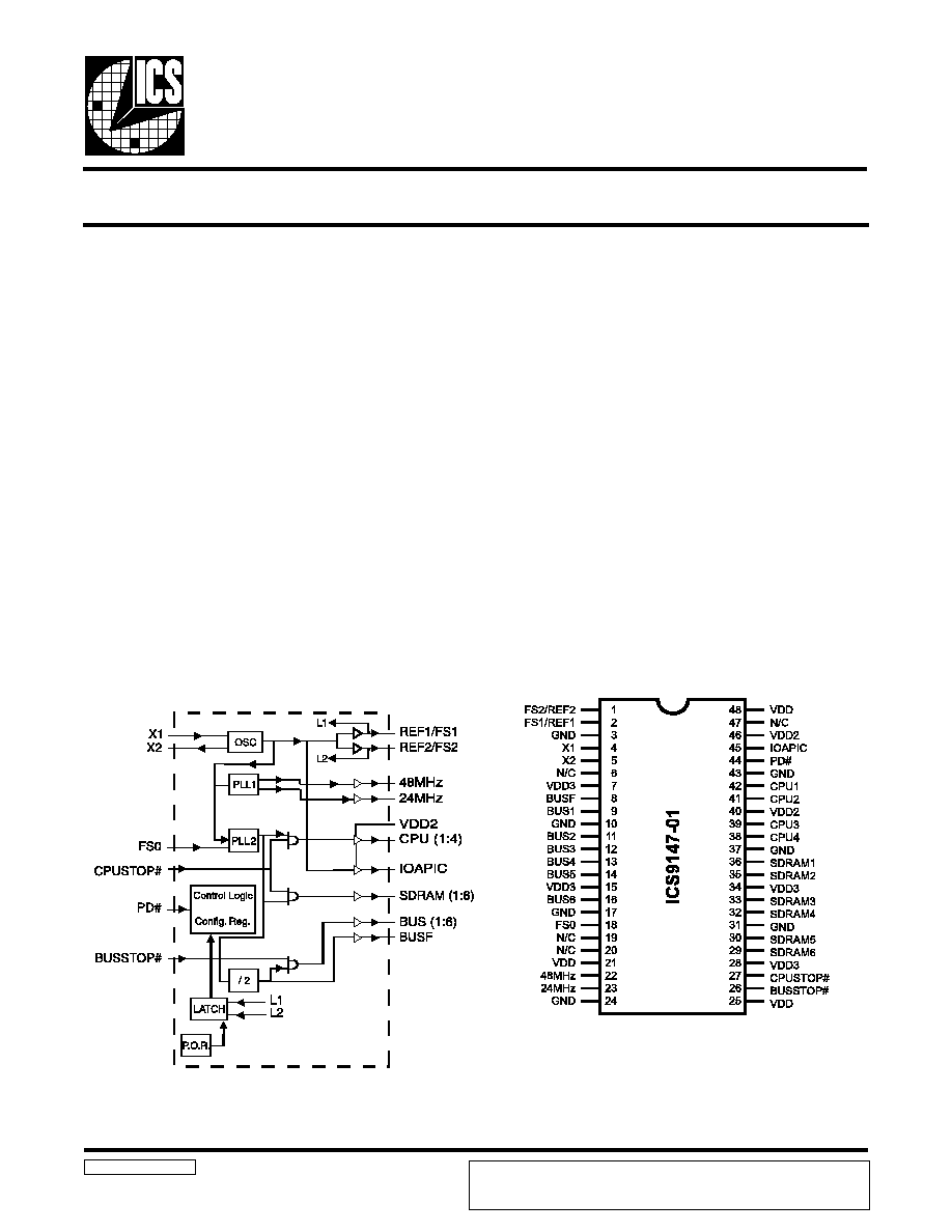
Block Diagram
Pentium is a trademark of Intel Corporation
Frequency Generator & Integrated Buffers for PENTIUM
TM
9147-01Rev B 04/25/01
Pin Configuration
The ICS9147-01 generates all clocks required for high
speed RISC or CISC microprocessor systems such as Intel
PentiumPro. Two bidirectional I/O pins (FS1,FS2) are latched
at power-on to the functionality table, with FS0 selectable
in real-time to toggle between conditions. The inputs
provide for tristate and test mode conditions to aid in
system level testing. These multiplying factors can be
customized for specific applications. Glitch-free stop
clockcontrols are provided for CPU clocks and BUS clocks.
High drive BUS and SDRAM outputs typically provide
greater than 1 V/ns slew rate into 30 pF loads. CPU outputs
typically provide better than 1V/ns slew rate into 20 pF
loads while maintaining
50 ±
5% duty cycle. The REF clock
outputs typically provide better than 0.5V/ns slew rates.
Seperate buffers supply pins VDD2 allow for 3.3V or
reduced voltage swing (from 2.9 to 2.5V) for CPU (1:4) and
IOAPIC outputs.
·
Four copies of CPU clock
·
Six SDRAM (3.3 V TTL), usable as AGP clocks
·
Seven copies of BUS clock (synchronous with CPU
clock/2 or CPU/2.5 for 75 and 83.3 MHz CPU)
·
CPU clocks to BUS clocks skew 1-4ns (CPU early)
·
One IOAPIC clock @14.31818 MHz
·
Two copies of Ref. clock @14.31818 MHz
·
One each 48/ 24 MHz (3.3 V TTL)
·
This device is configured into the Mobile mode for
power management of Intel 430 TX
·
Ref. 14.31818 M Hz Xtal oscillator input
·
Separate 66/60 MHz select pin (LSB of select pins)
·
Separate V
DD2
for four CPU and single IOAPIC output
buffers to allow 2.5V output (or Std. Vdd)
·
Power Management Control Input pins
·
3.0V 3.7V supply range w/2.5V compatible outputs
·
48-pin SSOP package
48-Pin SSOP
ICS reserves the right to make changes in the device data identified in this publication
without further notice. ICS advises its customers to obtain the latest version of all
device data to verify that any information being relied upon by the customer is current
and accurate.
4
ICS9147-01
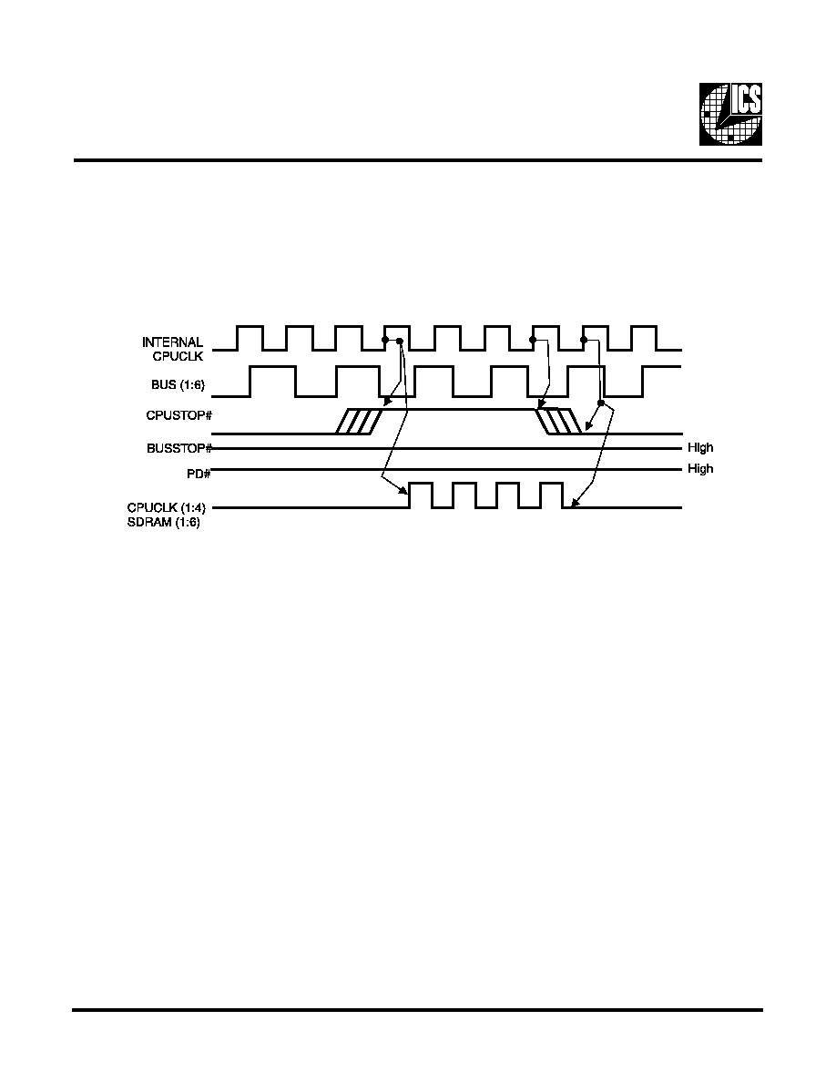
BUSSTOP# is an asynchronous input to the ICS9147-01. It is used to turn off the BUS (1:6) clocks for low power operation.
BUSSTOP# is synchronized by the ICS9147-01 internally. BUS (1:6) clocks are stopped in a low state and started with
a full high pulse width guaranteed. BUS (1:6) clock on latency cycles are less than 4 CPU clocks and BUS (1:6) clock off
latency is less than 4 clocks.
(Drawing shown on next page.)
Notes:
1. All timing is referenced to the internal CPU clock.
2. CPUSTOP# is an asynchronous input and metastable conditions
may exist. This signal is synchronized to the CPU and SDRAM
clocks inside the ICS9147-01.
3. All other clocks continue to run undisturbed.
4. PD# and BUSSTOP# are shown in a high (true) state.
CPUSTOP# Timing Diagram
CPUSTOP# is an asychronous input to the clock synthesizer. It is used to turn off the CPU clocks for low power operation.
CPUSTOP# is synchronized by the ICS9147-01. All other clocks will continue to run while the CPU and SDRAM clocks
are disabled. The CPU and SDRAM clocks will always be stopped in a low state and start in such a manner that guarantees
the high pulse width is a full pulse. CPU clock on latency is 0 to 1 CPU clocks and CPU clock off latency is 0 to 1 CPU
clocks.
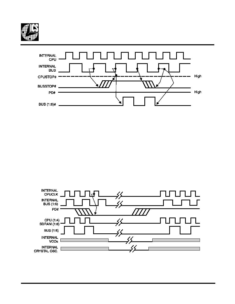
BUSSTOP # Timing Diagram
5
ICS9147- 01
Notes:
1. All timing is referenced to the Internal CPU clock (defined as inside the ICS9147 device).
2. PD# is an asynchronous input and metastable conditions may exist. This signal is synchronized inside the ICS9147.
3. The shaded sections on the VCO and the Crystal signals indicate an active clock is being generated.
The power down selection is used to put the part into a very low power state without turning off the power to the part.
PD# is an asynchronous active low input. This signal is synchronized internal by the ICS9147-01 prior to its control
action of powering down the clock synthesizer. PD# is an asynchronous function for powering up the system. Internal
clocks will not be running after the device is put in power down state. When PD# is active (low) all clocks are driven to
a low state and held prior to turning off the VCOs and the Crystal oscillator. The power on latency is guaranteed to be
less than 3mS. The power down latency is less than three CPU clock cycles. BUSSTOP# and CPUSTOP# are don't care
signals during the power down operations.
PD# Timing Diagram
Notes:
1. All timing is referenced to the Internal BUS clock (defined as inside the ICS9147 device.)
2. BUSSTOP# is an asynchronous input, and metastable conditions may exist. This signal is required to be
synchronized inside the ICS9147.
3. All other clocks continue to run undisturbed.
4. PD# and CPUSTOP# are shown in a high (true) state.