 | ÐлекÑÑоннÑй компоненÑ: HT48R50A | СкаÑаÑÑ:  PDF PDF  ZIP ZIP |
Äîêóìåíòàöèÿ è îïèñàíèÿ www.docs.chipfind.ru

HT48R50A-1
8-Bit Microcontroller
Rev. 1.10
1
July 2, 2001
General Description
This device is an 8-bit high performance
RISC-like microcontroller designed for multi-
ple I/O product applications. It is particularly
suitable for use in products such as remote con-
trollers, fan/light controllers, washing machine
controllers, scales, toys and various subsystem
controllers. A HALT feature is included to re-
duce power consumption.
Features
·
Operating voltage:
f
SYS
=4MHz: 3.3V~5.5V
f
SYS
=8MHz: 4.5V~5.5V
·
Low voltage reset function
·
35 bidirectional I/O lines (max.)
·
1 interrupt input shared with an I/O line
·
8-bit programmable timer/event counter with
overflow interrupt and 8-stage prescaler
·
16-bit programmable timer/event counter
and overflow interrupts
·
On-chip RC oscillator, external crystal and
RC oscillator
·
32768Hz crystal oscillator for timing
purposes only
·
Watchdog Timer
·
4096´15 program memory ROM
·
160´8 data memory RAM
·
Buzzer driving pair and PFD supported
·
HALT function and wake-up feature reduce
power consumption
·
6-level subroutine nesting
·
Up to 0.5ms instruction cycle with 8MHz
system clock at V
DD
=5V
·
Bit manipulation instruction
·
15-bit table read instruction
·
63 powerful instructions
·
All instructions in one or two machine
cycles
·
28-pin SKDIP/SOP, 48-pin SSOP package
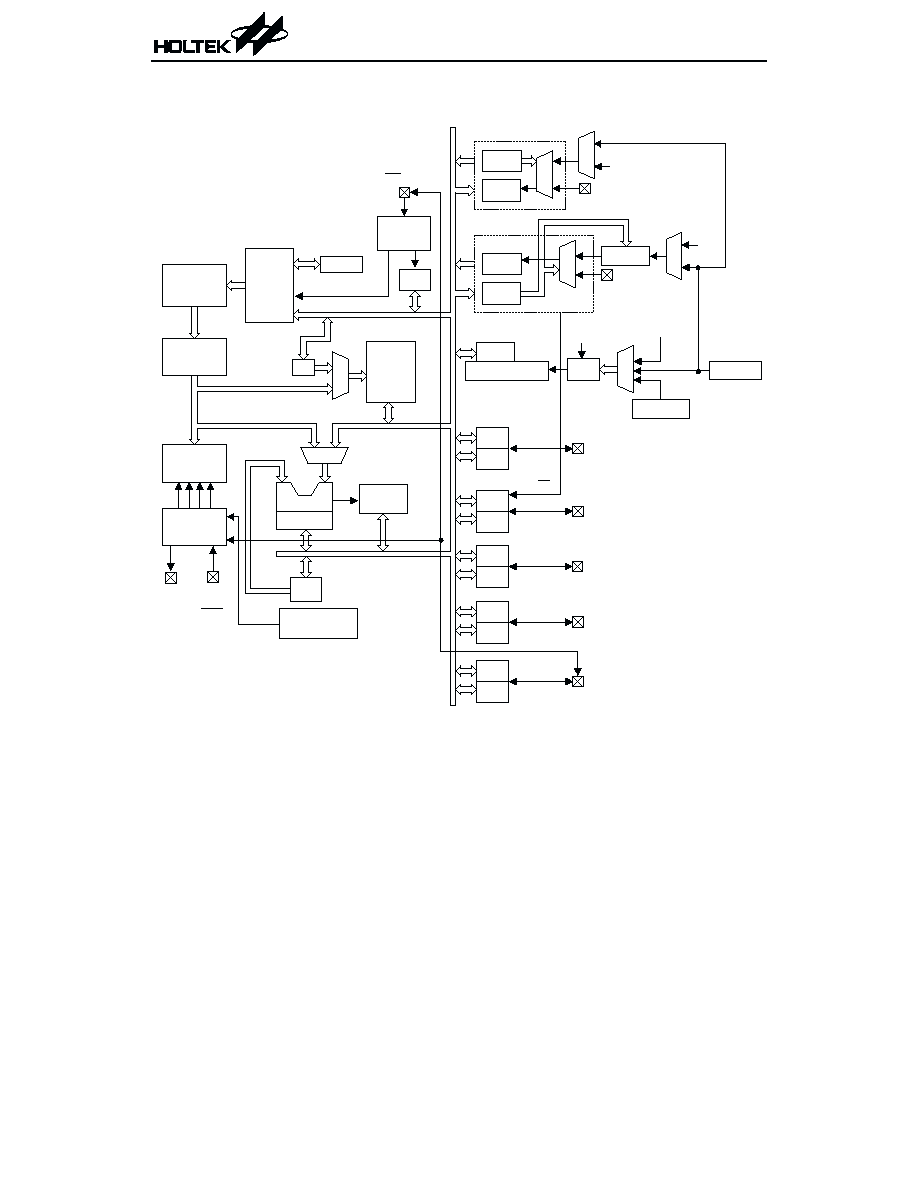
Block Diagram
HT48R50A-1
Rev. 1.10
2
July 2, 2001
I N T / P G 0
O S C 2 /
P G 2
O S C 1 /
P G 1
R E S
V D D
M U X
T M R 0
T M R 0 C
T M R 0
V S S
P r e s c a l e r
f
S Y S
P G 0
P r o g r a m
R O M
P r o g r a m
C o u n t e r
I n t e r r u p t
C i r c u i t
S T A C K
I N T C
D A T A
M e m o r y
I n s t r u c t i o n
R e g i s t e r
M
U
X
I n s t r u c t i o n
D e c o d e r
S T A T U S
A L U
S h i f t e r
T i m i n g
G e n e r a t o r
A C C
M
U
X
M P
S Y S C L K / 4
W D T S
W D T
W D T O S C
W D T P r e s c a l e r
M
U
X
R T C O S C
E N / D I S
P G 1
P G 2
I n t e r n a l
R C O S C
P D C
P O R T D
P D 0 ~ P D 7
P G C
P G
P O R T G
P G 0 ~ P G 2
P B C
P O R T B
P B 0 ~ P B 7
B Z / B Z
P B
P A C
P O R T A
P A 0 ~ P A 7
P A
P D
P C
P O R T C
P C 0 ~ P C 7
P C C
T M R 1 C
T M R 1
M
U
X
M
U
X
T M R 1
f
S Y S
/ 4
M
U
X
Pin Assignment
HT48R50A-1
Rev. 1.10
3
July 2, 2001
2 8
2 7
2 6
2 5
2 4
2 3
2 2
2 1
2 0
1 9
1 8
1 7
1 6
1 5
1
2
3
4
5
6
7
8
9
1 0
1 1
1 2
1 3
1 4
P B 6
P B 7
P A 4
P A 5
P A 6
P A 7
O S C 2 / P G 2
O S C 1 / P G 1
V D D
R E S
P C 5 / T M R 1
P C 4
P C 3
P C 2
P B 5
P B 4
P A 3
P A 2
P A 1
P A 0
P B 3
P B 2
P B 1 / B Z
P B 0 / B Z
V S S
P G 0 / I N T
P C 0 / T M R 0
P C 1
H T 4 8 R 5 0 A - 1
2 8 S K D I P - A / S O P - A
4 8
4 7
4 6
4 5
4 4
4 3
4 2
4 1
4 0
3 9
3 8
3 7
3 6
3 5
3 4
3 3
3 2
3 1
3 0
2 9
2 8
2 7
2 6
2 5
1
2
3
4
5
6
7
8
9
1 0
1 1
1 2
1 3
1 4
1 5
1 6
1 7
1 8
1 9
2 0
2 1
2 2
2 3
2 4
H T 4 8 R 5 0 A - 1
4 8 S S O P - A
P B 6
P B 7
P A 4
P A 5
P A 6
P A 7
N C
N C
N C
N C
O S C 2 / P G 2
O S C 1 / P G 1
V D D
R E S
T M R 1
P D 3
P D 2
P D 1
P D 0
P C 7
P C 6
P C 5
P C 4
P C 3
P B 5
P B 4
P A 3
P A 2
P A 1
P A 0
P B 3
P B 2
P B 1 / B Z
P B 0 / B Z
N C
N C
N C
N C
P D 7
P D 6
P D 5
P D 4
V S S
P G 0 / I N T
T M R 0
P C 0
P C 1
P C 2
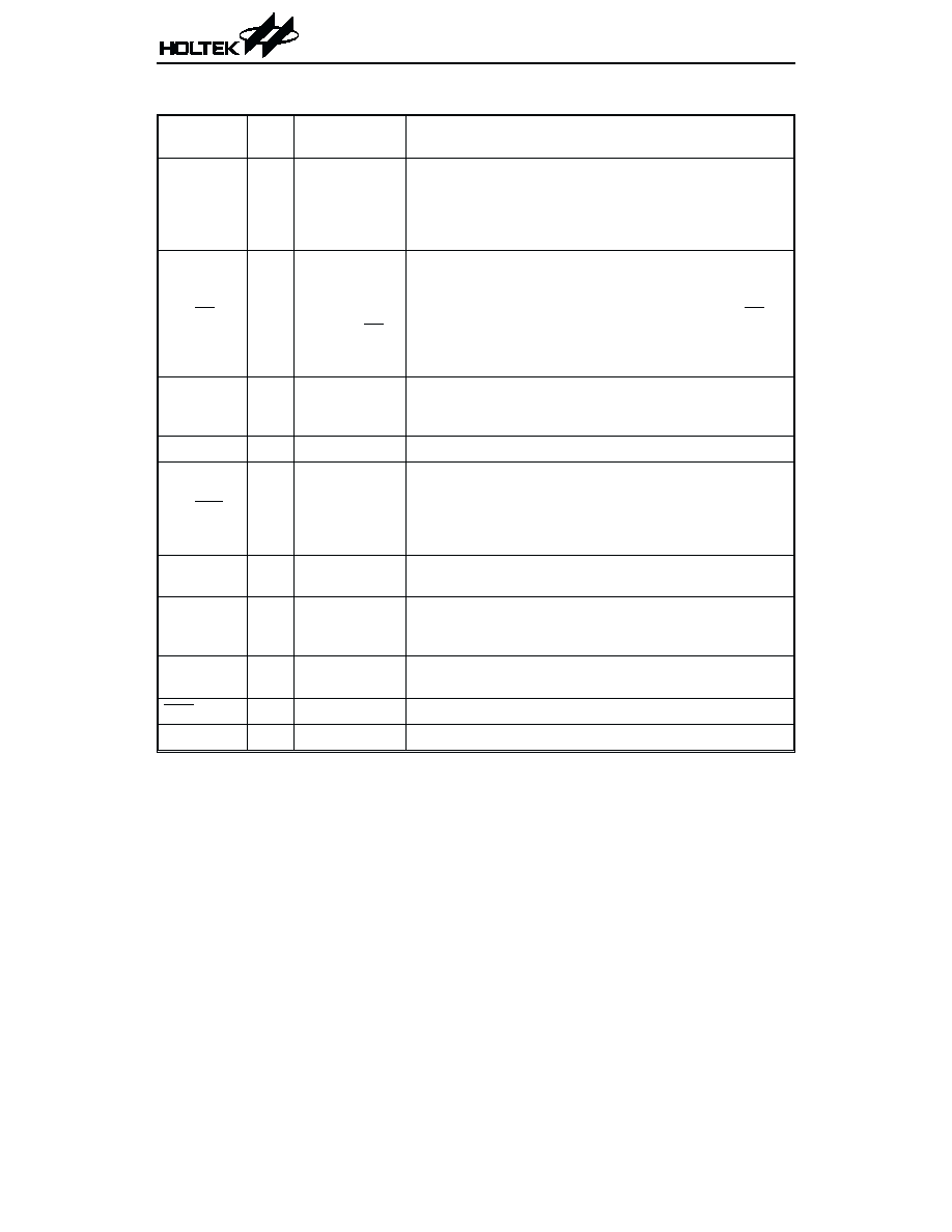
Pin Description
Pin Name
I/O
ROM Code
Option
Description
PA0~PA7
I/O
Pull-high*
Wake-up
CMOS/Schmitt
trigger input
Bidirectional 8-bit input/output port. Each bit can be con-
figured as a wake-up input by ROM code option. Software
instructions determine the CMOS output or Schmitt trigger
or CMOS input (depends on options) with pull-high resistor
(determined by 1-bit pull-high option).
PB0/BZ
PB1/BZ
PB2~PB7
I/O
Pull-high*
PB0 or BZ
PB1 or BZ
Bidirectional 8-bit input/output port. Software instructions
determine the CMOS output or Schmitt trigger input with
pull-high resistor (determined by 1-bit pull-high option).
The PB0 and PB1 are pin-shared with the BZ and BZ, re-
spectively. Once the PB0 or PB1 is selected as buzzer out-
put, the output signals come from an internal PFD
generator (shared with Timer/Event Counter 0).
PD0~PD7
I/O
Pull-high*
Bidirectional I/O lines. Software instructions determine the
CMOS output or Schmitt trigger input with pull-high resis-
tor (determined by 1-bit pull-high option).
VSS
¾
¾
Negative power supply, ground
PG0/INT
I/O
Pull-high*
Bidirectional I/O lines. Software instructions determine the
CMOS output or Schmitt trigger input with pull-high resis-
tor (determined by 1-bit pull-high option). This external in-
terrupt input is pin-shared with PG0. The external
interrupt input is activated on a high to low transition.
TMR0
I
¾
Timer/Event Counter 0 Schmitt trigger input (without
pull-high resistor)
PC0~PC7
I/O
Pull-high*
Bidirectional I/O lines. Software instructions determine the
CMOS output or Schmitt trigger input with pull-high resis-
tor (determined by 1-bit pull-high option).
TMR1
I
¾
Timer/Event Counter 1 Schmitt trigger input (without
pull-high resistor)
RES
I
¾
Schmitt trigger reset input. Active low
VDD
¾
¾
Positive power supply
HT48R50A-1
Rev. 1.10
4
July 2, 2001
Pin Name
I/O
ROM Code
Option
Description
OSC1/PG1
OSC2/PG2
I
O
Pull-high*
Crystal or RC
or Int. RC+I/O
or Int. RC+RTC
OSC1, OSC2 are connected to an RC network or Crystal
(determined by ROM code option) for the internal system
clock. In the case of RC operation, OSC2 is the output termi-
nal for 1/4 system clock. These two pins can also be optioned
as an RTC oscillator (32768Hz) or I/O lines. In these two
cases, the system clock comes from an internal RC oscillator
whose frequency has 4 options (3.2MHz, 1.6MHz, 800kHz,
400kHz). If the I/O option is selected, the pull-high options
can also be enabled or disabled. Otherwise the PG1 and
PG2 are used as internal registers (pull-high resistors are
always disabled).
Note: * The pull-high resistors of each I/O port (PA, PB, PC, PD, PG) are controlled by a ROM code
options.
or Schmitt trigger option of port A is controlled by a ROM code option.
Absolute Maximum Ratings
Supply Voltage ...............V
SS
-0.3V to V
SS
+5.5V
Storage Temperature ................-50°C to 125°C
Input Voltage.................V
SS
-0.3V to V
DD
+0.3V
Operating Temperature ..............-40°C to 85°C
Note: These are stress ratings only. Stresses exceeding the range specified under "Absolute Maxi-
mum Ratings" may cause substantial damage to the device. Functional operation of this device
at other conditions beyond those listed in the specification is not implied and prolonged expo-
sure to extreme conditions may affect device reliability.
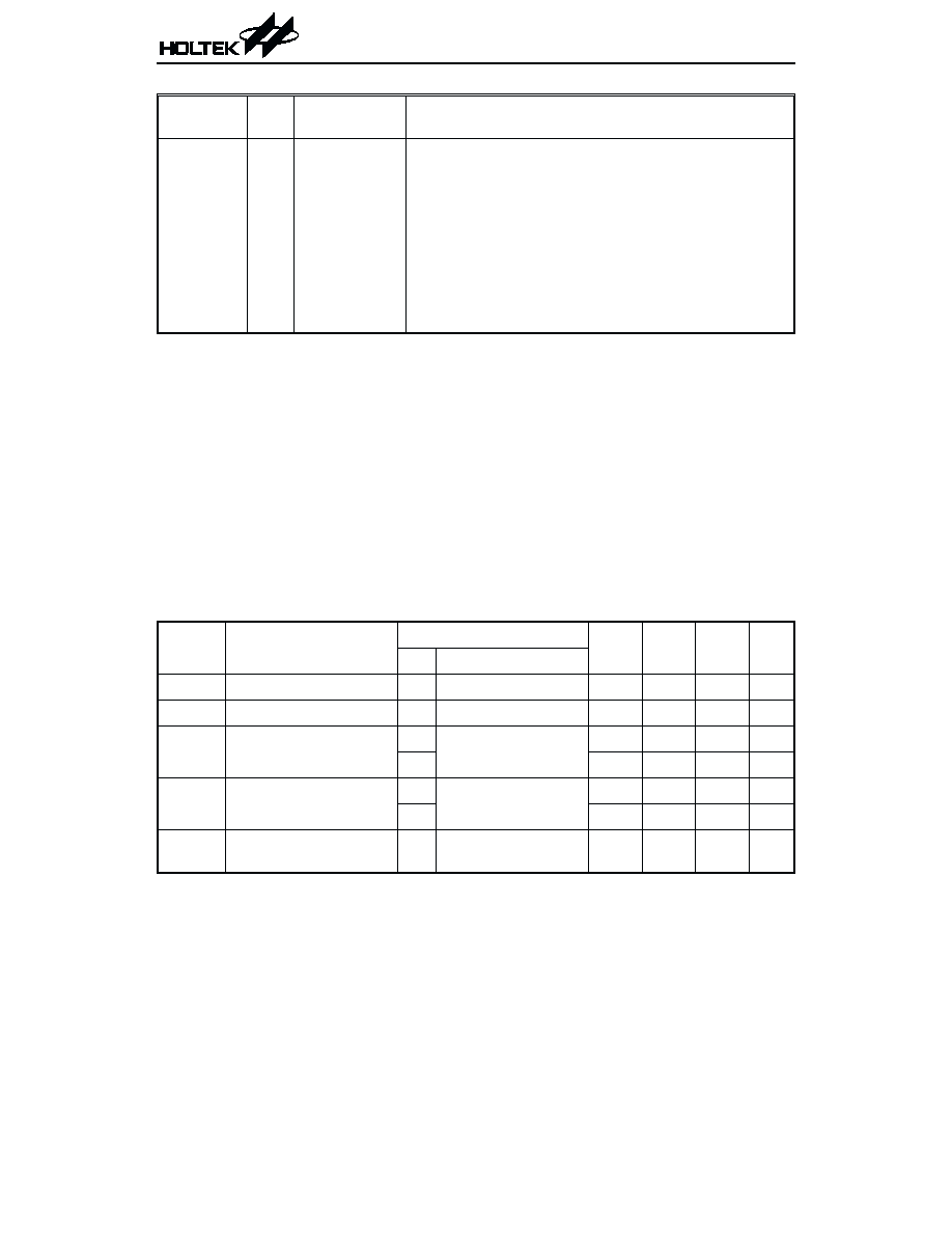
D.C. Characteristics
Ta=25°C
Symbol
Parameter
Test Conditions
Min.
Typ.
Max. Unit
V
DD
Conditions
V
DD1
Operating Voltage
¾ f
SYS
=4MHz
3.3
¾
5.5
V
V
DD2
Operating Voltage
¾ f
SYS
=8MHz
4.5
¾
5.5
V
I
DD1
Operating Current
(Crystal OSC)
3.3V
No load, f
SYS
=4MHz
¾
1
2
mA
5V
¾
3
5
mA
I
DD2
Operating Current
(RC OSC)
3.3V
No load, f
SYS
=4MHz
¾
1
2
mA
5V
¾
3
5
mA
I
DD3
Operating Current
(Crystal OSC)
5V No load, f
SYS
=8MHz
¾
4
8
mA
HT48R50A-1
Rev. 1.10
5
July 2, 2001
Document Outline
- þÿ
- þÿ
- þÿ
- þÿ
- þÿ
- þÿ
- þÿ
- þÿ
- þÿ
- þÿ
- þÿ
- þÿ