 | ÐлекÑÑоннÑй компоненÑ: PZTA55 | СкаÑаÑÑ:  PDF PDF  ZIP ZIP |
Äîêóìåíòàöèÿ è îïèñàíèÿ www.docs.chipfind.ru
MPSA55
/
MMBT
A55
/
PZT
A
5
5
PNP General Purpose Amplifier
This device is designed for general purpose amplifier applications
at collector currents to 300 mA. Sourced from Process 73. See
MPSA56 for characteristics.
Absolute Maximum Ratings*
TA = 25°C unless otherwise noted
*
These ratings are limiting values above which the serviceability of any semiconductor device may be impaired.
NOTES:
1) These ratings are based on a maximum junction temperature of 150 degrees C.
2) These are steady state limits. The factory should be consulted on applications involving pulsed or low duty cycle operations.
Symbol
Parameter
Value
Units
V
CES
Collector-Emitter Voltage
60
V
V
CBO
Collector-Base Voltage
60
V
V
EBO
Emitter-Base Voltage
4.0
V
I
C
Collector Current - Continuous
500
mA
T
J
, T
stg
Operating and Storage Junction Temperature Range
-55 to +150
°
C
Thermal Characteristics
TA = 25°C unless otherwise noted
Symbol
Characteristic
Max
Units
MPSA55
*MMBTA55
**PZTA55
P
D
Total Device Dissipation
Derate above 25
°
C
625
5.0
350
2.8
1,000
8.0
mW
mW/
°
C
R
JC
Thermal Resistance, Junction to Case
83.3
°
C/W
R
JA
Thermal Resistance, Junction to Ambient
200
357
125
°
C/W
*
Device mounted on FR-4 PCB 1.6" X 1.6" X 0.06."
**
Device mounted on FR-4 PCB 36 mm X 18 mm X 1.5 mm; mounting pad for the collector lead min. 6 cm
2
.
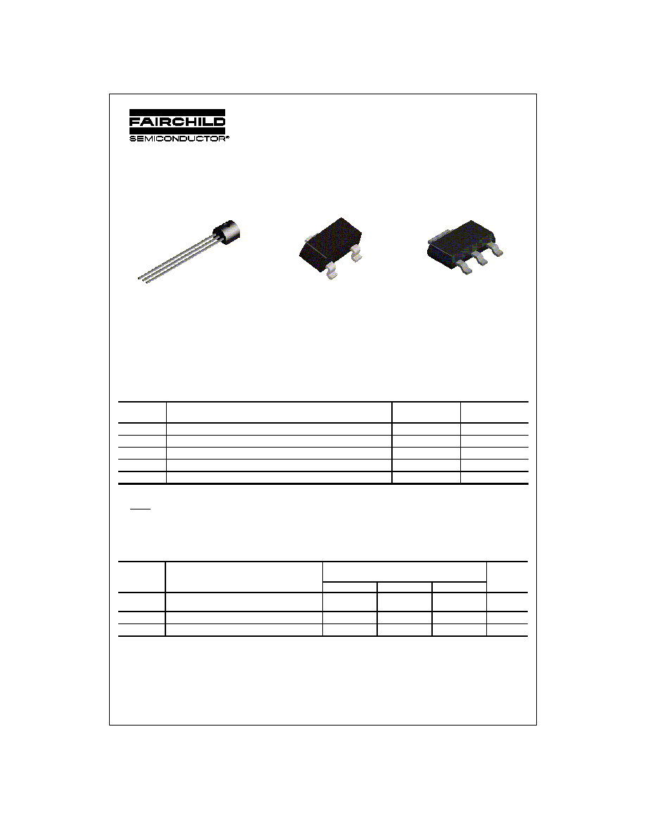
MPSA55
C
B E
TO-92
MMBTA55
C
B
E
SOT-23
Mark: 2H
PZTA55
B
C
C
SOT-223
E
ã 1997 Fairchild Semiconductor Corporation
MPSA55/MMBTA55/PZTA55, Rev A
MPSA55
/
MMBT
A55
/
PZT
A
5
5
Electrical Characteristics
TA = 25°C unless otherwise noted
OFF CHARACTERISTICS
Symbol
Parameter
Test Conditions
Min
Max
Units
V
(BR)CEO
Collector-Emitter Breakdown
Voltage*
I
C
= 1.0 m A, I
B
= 0
60
V
V
(BR)CBO
Collector-Base Breakdown Voltage
I
C
= 100
µ
A, I
E
= 0
60
V
V
(BR)EBO
Emitter-Base Breakdown Voltage
I
E
= 100
µ
A, I
C
= 0
4.0
V
I
CEO
Collector-Cutoff Current
V
CE
= 60 V, I
B
= 0
0.1
µ
A
I
CBO
Collector-Cutoff Current
V
CB
= 60 V, I
E
= 0
0.1
µ
A
ON CHARACTERISTICS
h
FE
DC Current Gain
I
C
= 10 mA, V
CE
= 1.0 V
I
C
= 100 mA, V
CE
= 1.0 V
100
100
V
CE(
sat
)
Collector-Emitter Saturation Voltage
I
C
= 100 mA, I
B
= 10 mA
0.25
V
V
BE(
on
)
Base-Emitter On Voltage
I
C
= 100 mA, V
CE
= 1.0 V
1.2
V
SMALL SIGNAL CHARACTERISTICS
f
T
Current Gain - Bandwidth Product
I
C
= 100 mA, V
CE
= 1.0 V,
f = 100 MHz
50
MHz
*
Pulse Test: Pulse Width £ 300 ms, Duty Cycle £ 2.0%
PNP General Purpose Amplifier
(continued)
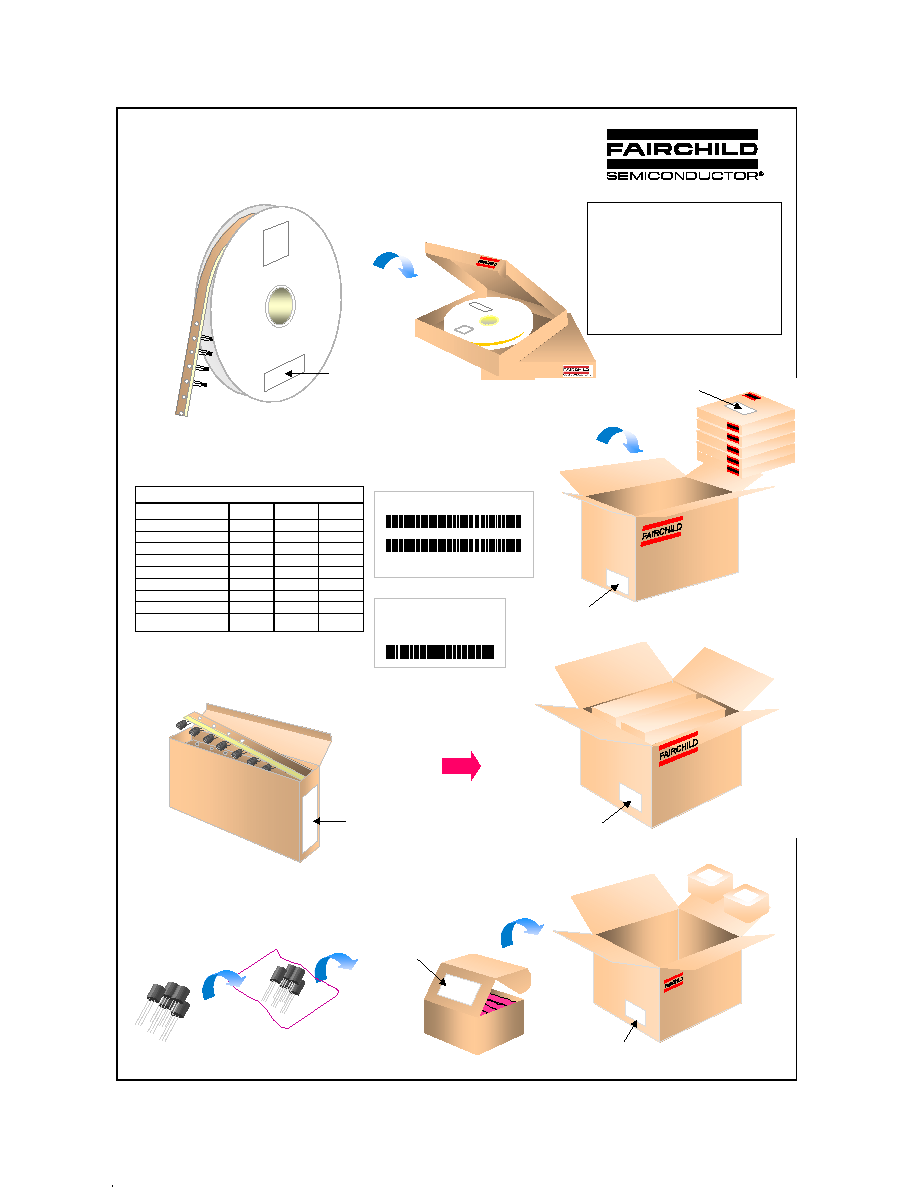
FKS Label
237mm x 167mm x 96mm
Bulk Inner box(10,000cap)
1,000 units per
Bulk Vinyl bag
10 Vinyl bags per
Inner box
525mm x 360mm x 265mm
Outer box(100,000cap)
FKS Label
525mm x 360mm x 265mm
Outer box(100,000cap)
FKS Label
TO-92 Bulk Packing
Configuration: Figure 4.0
TO-92 Tape and Reel Data
©2001 Fairchild Semiconductor Corporation
October 2001, Rev. A
TO-92 Packaging
Configuration: Figure 1.0
FKS Label
1 Reel per
Inner box
395mm x 375mm x 56mm
Inner box(2,000cap)
395mm x 375mm x 56mm
Inner box(2,000cap)
Packaging Description:
TO-92 parts are shipped normally in tape. These reeled
parts in standard option are shipped with 2,000 units per
14" or 355.6cm diameter reel. This and some other options
are further described in the Packaging Information
table.These full reels are individually barcode labeled and
placed inside a standard intermediate box (illustrated in
figure 1.0) made of recyclable corrugated brown paper.
One box contains one reel maximum. And these boxes
are placed inside a barcode labeled shipping box which
comes in different sizes depending on the number of parts
shipped.
01
FKS Label
525mm x 360m x 265mm
Outer box (30,000cap)
420mm x 420mm x 320mm
Outer box(10,000cap)
FKS Label
FKS Label
DVC:
KA7812-AE
LOT:
IMSYS777
Q'TY:
12000
Outer Box Bar Code Label Sample
IM
01
A710103105
88706892
7103
DVC:
KA7812-AE
LOT:
IMSYS777
12000
IM
01
00 / 03 / 17
07:30
DVC:
LOT:
Q'TY:
Inner Box Bar Code Label Sample
DVC:
KA7812-AE
OPTION:
TKLEE777
1000
00 / 03 / 17
06:30
W/W: 0103
01
20000025
MBB : NOR P/U : 660
S/T : LOGO I/B: LOGO
HIC : 0 P/T:O MIX: X
P
ETC:
Note/Comments
Packaging Option
TO-92 Packaging Information
Standard
(no flow code)
Packaging type
TNR
Qty per Reel/Tube/ Bag
2,000
Inner Box Dimension (mm)
395x375x56
Max qty per Box
2,000
Weight per unit (gm)
0.2080
Outer Box Dimension (mm) 420x420x320
Max qty per Box
10,000
Standard
(no flow code)
AMMO
328x162x43
2,000
0.2080
525x360x265
30,000
Standard
(no flow code)
BULK
1,000
237x167x96
10,000
0.2080
525x360x265
100,000
Reel Size
14" Dia
-
-
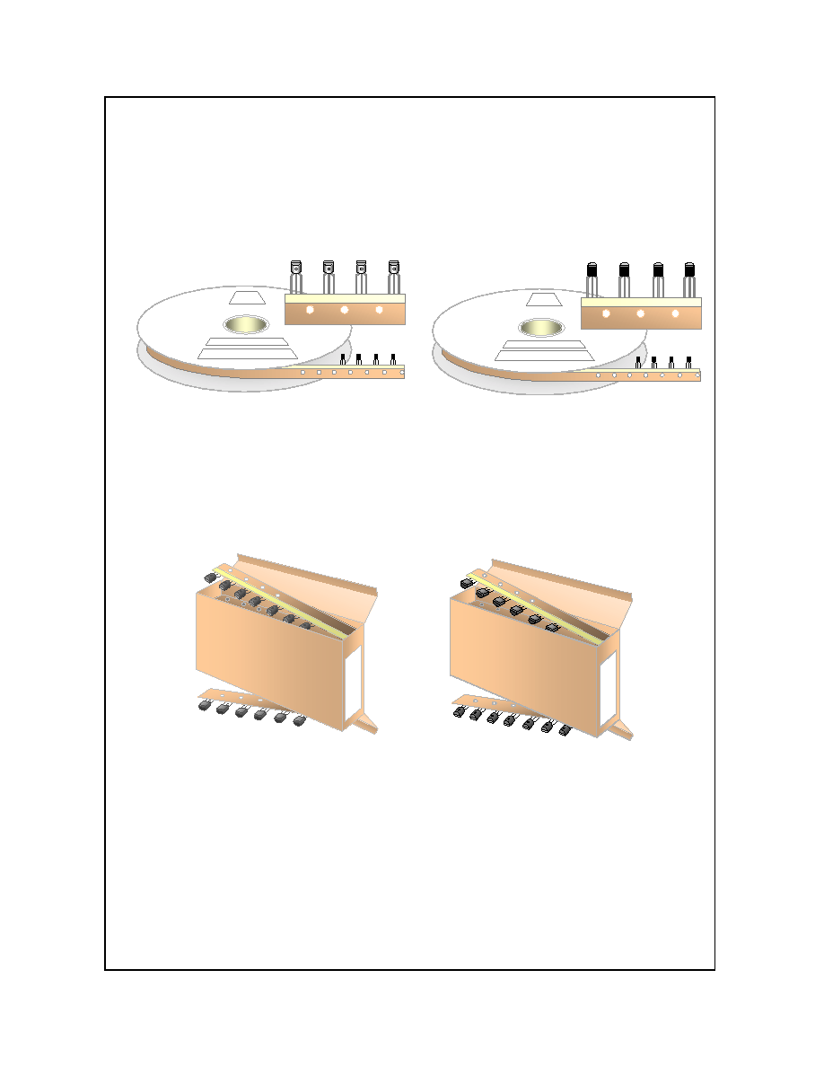
TO-92 Packaging
Configuration: Figure 2.0
TO-92 AMMO Packaging
Configuration: Figure 3.0
15 Ammo boxes per
Outer Box
328mm x 162mm x 43mm
Inner box (2,000cap)
FKS Label
328mm x 162mm x 43mm
Inner box (2,000cap)
FKS Label
TO-92 Tape and Reel Data, continued
October 2001, Rev. A
TO-92 Reeling Style
Configuration: Figure 5.0
Standard
Machine Option
FIRST WIRE OFF IS EMITTER
ADHESIVE TAPE IS ON THE TOP SIDE
FLAT OF TRANSISTOR IS ON BOTTOM
FIRST WIRE OFF IS COLLECTOR
ADHESIVE TAPE IS ON BOTTOM SIDE
FLAT OF TRANSISTOR IS ON TOP
FIRST WIRE OFF IS EMITTER
ADHESIVE TAPE IS ON THE TOP SIDE
FLAT OF TRANSISTOR IS ON BOTTOM
FIRST WIRE OFF IS COLLECTOR
ADHESIVE TAPE IS ON BOTTOM SIDE
FLAT OF TRANSISTOR IS ON TOP
FIRST WIRE OFF IS COLLECTOR
ADHESIVE TAPE IS ON THE TOP SIDE
FLAT OF TRANSISTOR IS ON TOP
FIRST WIRE OFF IS EMITTER
ADHESIVE TAPE IS ON BOTTOM SIDE
FLAT OF TRANSISTOR IS ON BOTTOM
FIRST WIRE OFF IS COLLECTOR
ADHESIVE TAPE IS ON THE TOP SIDE
FLAT OF TRANSISTOR IS ON TOP
FIRST WIRE OFF IS EMITTER
ADHESIVE TAPE IS ON BOTTOM SIDE
FLAT OF TRANSISTOR IS ON BOTTOM
TO-92 Radial Ammo Packaging
Configuration: Figure 6.0
Standard
Machine Option
TO-92 Tape and Reel Data, continued
October 2001, Rev. A
TO-92 Tape and Reel Taping
Dimension Configuration: Figure 7.0
H1
H
HO
PO
P2
P1 F1
DO
P
d
J1
WO
W1
W
t
T
W2
User Direction of Feed
User Direction of Feed
A
A1
F2
jh
TO-92 Reel
Configuration: Figure 8.0
SENSITIVE DEV ICES
ELECTROSTATIC
SENSITIVE DEV ICES
ELECTROSTATIC
D1
FKS Label
W2
W1
W3
D4
D2
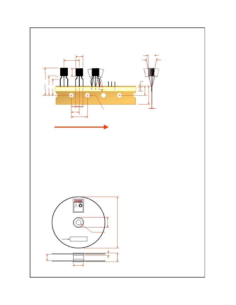
ITEM DESCRIPTION
Body Width
Body Height
Body Thickness
Lead-Wire Diameter
Pitch of Component
Feed Hole Pitch
Hole Center to Component Center
Lead to Lead Distance
Component Alignment F-R
Tape Width
Hole-Down Tape Width
Hole Position
Hole-Down Tape Position
Height of Component From Tape Center
Lead-Wire Clinch Height
Component Height
Lead-Wire (Tape Portion)
Feed Hole Diameter
Total Tape Thickness
Position of Hole
SYMBOL
A1
A
T
d
P
P0
P2
F1,F2
jh
W
W0
W1
W2
H
H0
H1
J1
D0
t
P1
DIMENSION
4.58 (+ 0.25, - 0.15)
4.58 (+/- 0.20)
3.86 (max)
0.46 (+/- 0.05)
12.7 (+/- 0.50)
12.7 (+/ -0.20)
6.35 (+/- 0.50)
2.50 (+ 0.3, - 0.10)
0.00 (+/- 1.00)
18.00 (+ 1.00, - 0.50)
6.00 (+/- 0.50)
9.00 (+/ -0.50)
1.00 (max)
19.50 (+/- 1.00)
16.00 (+/- 0.50)
27.0 (max)
2.50 (min)
4.00 (+/- 0.20)
0.65 (+/- 0.20)
3.85 (+/- 0.50)
Note : All dimensions are in millimeters.
REMARK
In Case of Reel
Package +/- 1.00
F1-F2= +/- 0.30
H + A <= H1
ITEM DESCRIPTION
SYSMBOL
MINIMUM
MAXIMUM
Reel Diameter
D1
13.975
14.025
Arbor Hole Diameter (Standard)
D2
1.160
1.200
(Small Hole)
D2
0.650
0.700
Core Diameter
D3
3.100
3.300
Hub Recess Inner Diameter
D4
2.700
3.100
Hub Recess Depth
W1
0.370
0.570
Flange to Flange Inner Width
W2
1.630
1.690
Hub to Hub Center Width
W3
2.090
Note: All dimensions are inches