©2002 Fairchild Semiconductor Corporation
Rev. A4, October 2002
KSH210
PNP Epitaxial Silicon Transistor
Absolute Maximum Ratings
T
C
=25
°
C unless otherwise noted
Electrical Characteristics
T
C
=25
°
C unless otherwise noted
* Pulse Test: PW
300
µ
s, Duty Cycle
2%
Symbol
Parameter
Value
Units
V
CBO
Collector-Base Voltage
- 40
V
V
CEO
Collector-Emitter Voltage
- 25
V
V
EBO
Emitter-Base Voltage
- 8
V
I
C
Collector Current (DC)
- 5
A
I
CP
Collector Peck Current (Pulse)
- 10
A
I
B
Base Current
- 1
A
P
C
Collector Dissipation (T
C
= 25
°
C)
12.5
W
Collector Dissipation (T
a
= 25
°
C)
1.4
W
T
J
Junction Temperature
150
°
C
T
STG
Storage Temperature
- 65 ~ 150
°
C
Symbol
Parameter
Test Condition
Min.
Max.
Units
V
CEO
(sus)
* Collector-Emitter Sustaining Voltage
I
C
= - 10mA, I
B
= 0
-25
V
I
CBO
Collector Cut-off Current
V
CB
= - 40V, I
E
= 0
-100
nA
I
EBO
Emitter Cut-off Current
V
EBO
= - 8V, I
C
= 0
-100
nA
h
FE
* DC Current Gain
V
CE
= - 1V, I
C
= - 500mA
V
CE
= - 1V, I
C
= - 2A
V
CE
= - 2V, I
C
= - 5A
70
45
10
180
V
CE
(sat)
* Collector-Emitter Saturation Voltage
I
C
= - 500mA, I
B
= - 50mA
I
C
= - 2A, I
B
= - 200mA
I
C
= - 5A, I
B
= - 1A
-0.3
-0.75
-1.8
V
V
V
V
BE
(sat)
* Base-Emitter Saturation Voltage
I
C
= - 5A, I
B
= - 1A
-2.5
V
V
BE
(on)
* Base-Emitter On Voltage
V
CE
= - 1V, I
C
= - 2A
-1.6
V
f
T
Current Gain Bandwidth Product
V
CE
= - 10V, I
C
= - 100mA
65
MHz
C
ob
Output Capacitance
V
CB
= - 10V, I
E
= 0, f = 0.1MHz
120
pF
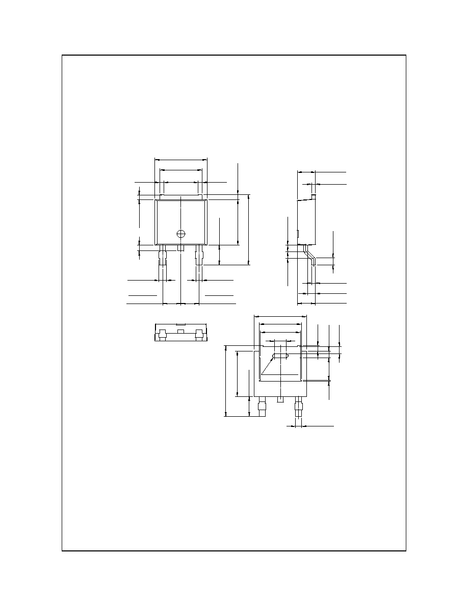
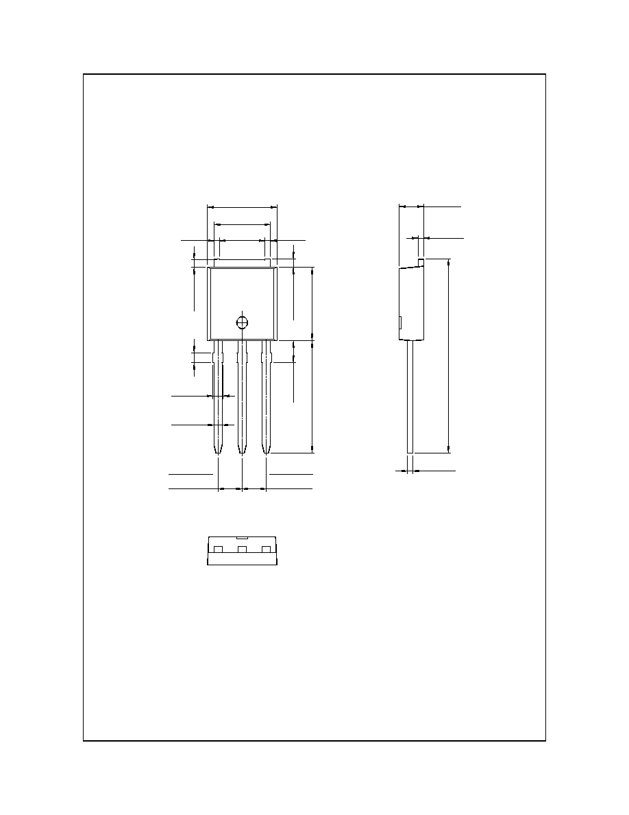
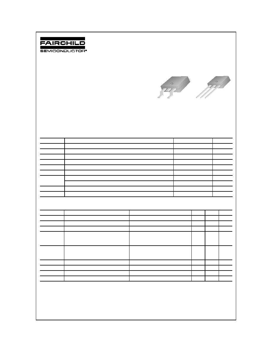
KSH210
D-PAK for Surface Mount Applications
· High DC Current Gain
· Low Collector Emitter Saturation Voltage
· Lead Formed for Surface Mount Applications (No Suffix)
· Straight Lead (I-PAK, " - I " Suffix)
1.Base 2.Collector 3.Emitter
D-PAK
I-PAK
1
1
©2002 Fairchild Semiconductor Corporation
KSH210
Rev. A4, October 2002
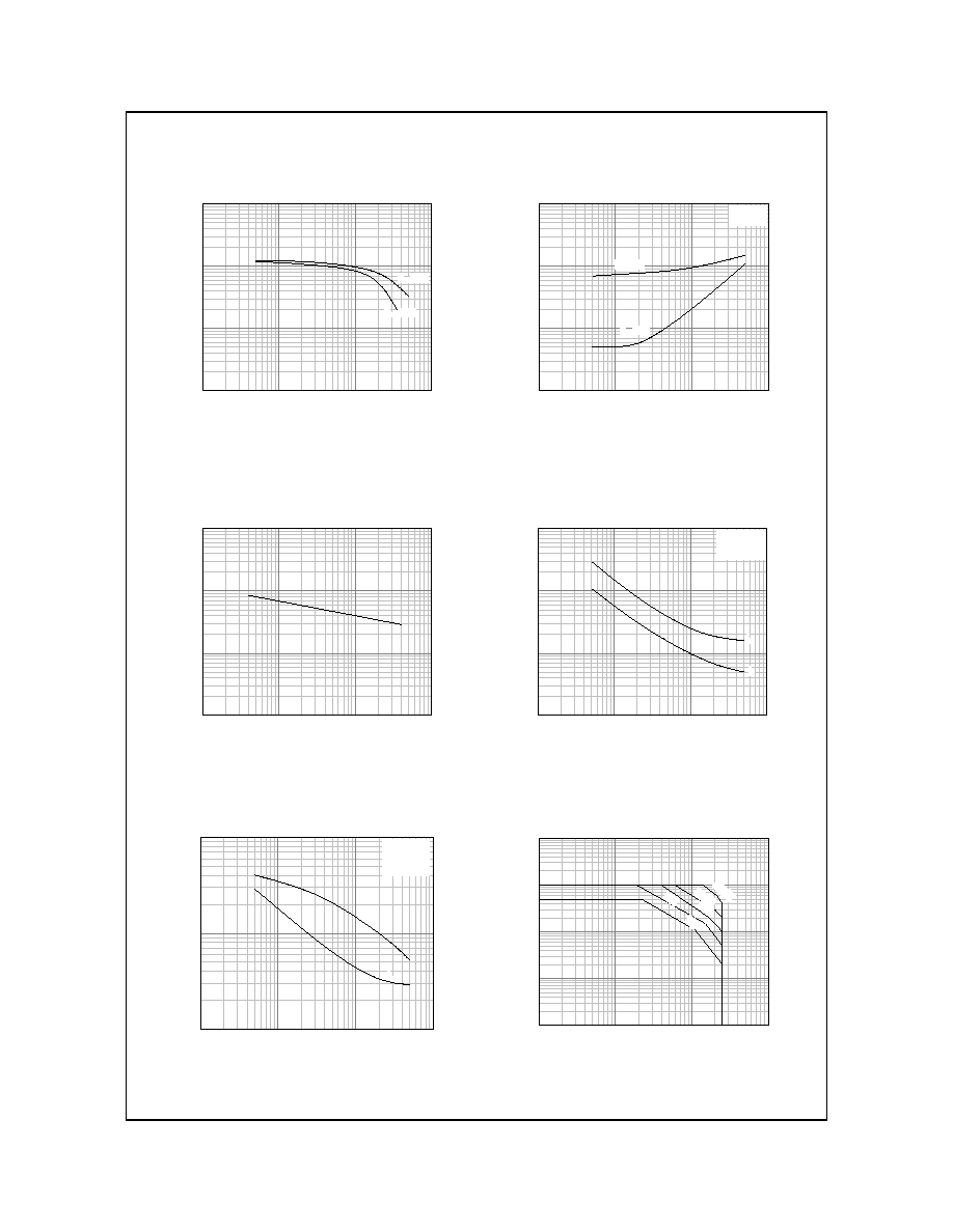
Typical Characteristics
Figure 1. DC current Gain
Figure 2. Base-Emitter Saturation Voltage
Collector-Emitter Saturation Voltage
Figure 3. Collector Output Capacitance
Figure 4. Turn On Time
Figure 5. Turn Off Time
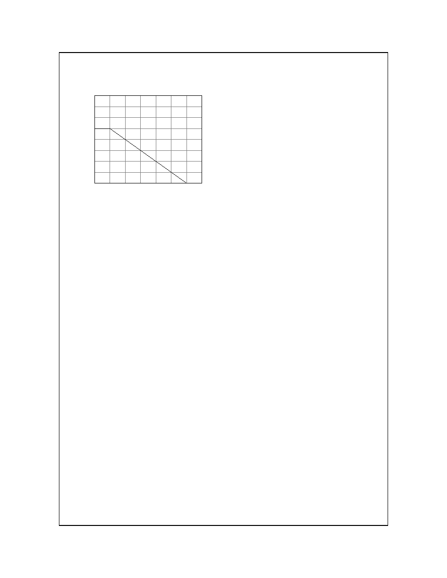
Figure 6. Safe Operating Area
-0.01
-0.1
-1
-10
1
10
100
1000
V
CE
=-1V
V
CE
=-2V
h
FE
, DC C
URRE
NT
G
A
I
N
I
C
[A], COLLECTOR CURRENT
-0.01
-0.1
-1
-10
-0.01
-0.1
-1
-10
I
C
=10I
B
V
BE
(sat)
V
CE
(sat)
V
CE
(s
a
t
),
V
BE
(
s
a
t
)
[
V
]
,
SAT
U
R
AT
I
O
N VO
L
T
AG
E
I
C
[A], COLLECTOR CURRENT
-0.1
-1
-10
-100
1
10
100
1000
C
ob
[pF
], C
A
P
A
CI
T
A
NCE
V
CB
[V], COLLECTOR BASE VOLTAGE
-0.01
-0.1
-1
-10
0.01
0.1
1
10
t
D
t
R
V
CC
=-30V
I
C
=10I
B
t
R
,t
D
[n
s], T
URN
ON
T
I
ME
I
C
[A], COLLECTOR CURRENT
-0.01
-0.1
-1
-10
10
100
1000
t
F
t
STG
V
CC
=-30V
I
C
=10I
B
I
B1
=-I
B2
t
ST
G
,t
F
[n
s
]
,
T
U
R
N
O
F
F
T
I
M
E
I
C
[A], COLLECTOR CURRENT
-0.1
-1
-10
-100
-0.01
-0.1
-1
-10
-100
DC
5m
s
1m
s
50
0
µ
s
10
0
µ
s
I
C
[A], CO
L
L
ECT
O
R CU
RRENT
V
CE
[V], COLLECTOR-EMITTER VOLTAGE