© 2000 Fairchild Semiconductor Corporation
DS006411
www.fairchildsemi.com
August 1986
Revised March 2000
DM74LS240
∑ D
M
74LS24
1
Oct
a
l 3-ST
A
T
E
Buf
f
er
/Li
ne Dri
ver/
L
ine Recei
ver
DM74LS240 ∑ DM74LS241
Octal 3-STATE Buffer/Line Driver/Line Receiver
General Description
These buffers/line drivers are designed to improve both the
performance and PC board density of 3-STATE buffers/
drivers employed as memory-address drivers, clock driv-
ers, and bus-oriented transmitters/receivers. Featuring
400 mV of hysteresis at each low current PNP data line
input, they provide improved noise rejection and high
fanout outputs and can be used to drive terminated lines
down to 133
.
Features
s
3-STATE outputs drive bus lines directly
s
PNP inputs reduce DC loading on bus lines
s
Hysteresis at data inputs improves noise margins
s
Typical I
OL
(sink current)
24 mA
s
Typical I
OH
(source current)
-
15 mA
s
Typical propagation delay times
Inverting
10.5 ns
Noninverting
12 ns
s
Typical enable/disable time 18 ns
s
Typical power dissipation (enabled)
Inverting
130 mW
Noninverting
135 mW
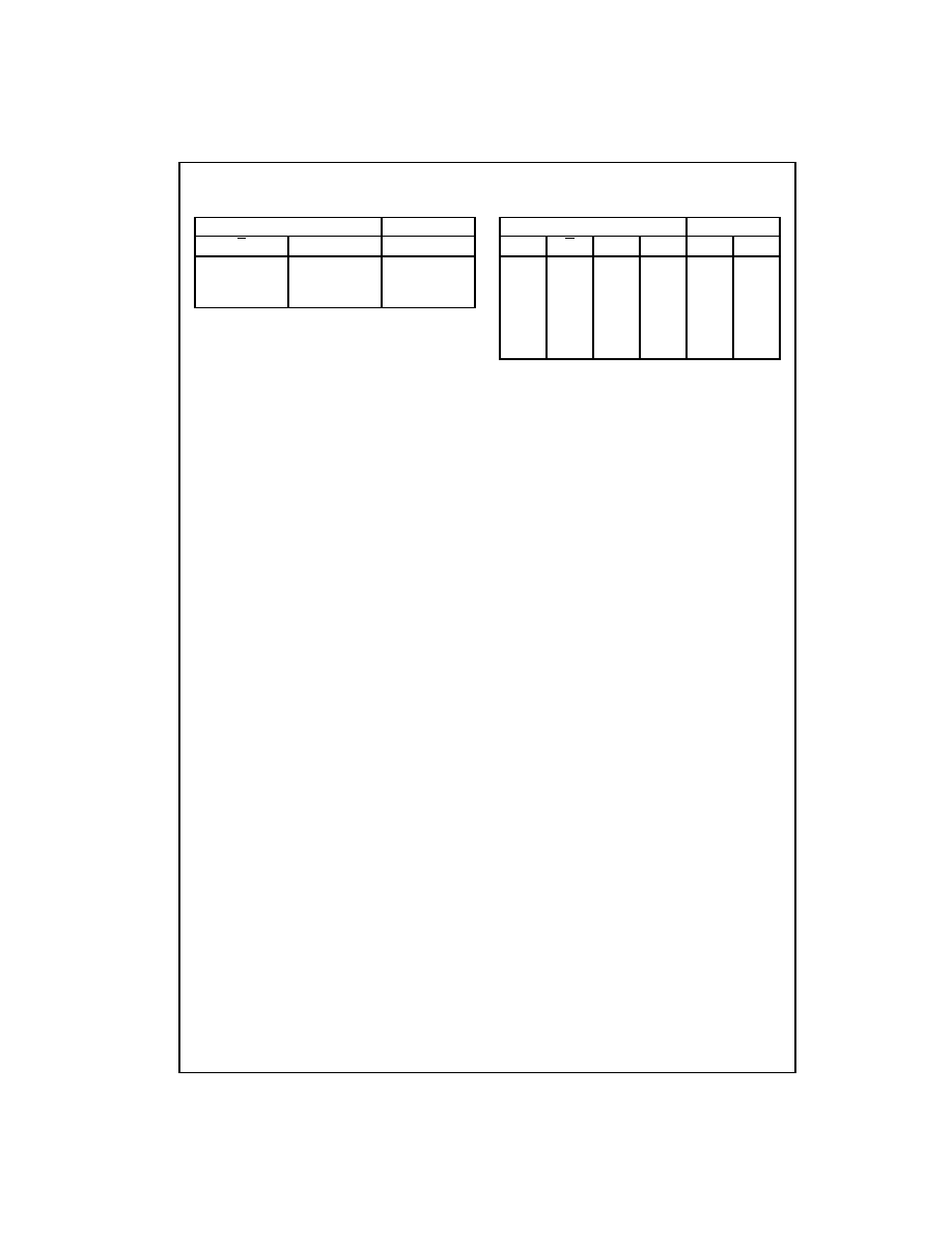
Ordering Code:
Devices also available in Tape and Reel. Specify by appending the suffix letter "X" to the ordering code.
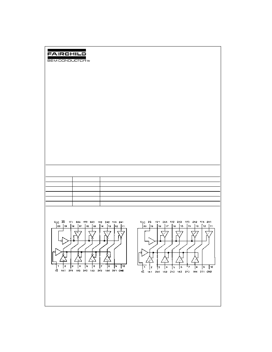
Connection Diagrams
DM74LS240
DM74LS241
Order Number
Package Number
Package Description
DM74LS240WM
M20B
20-Lead Small Outline Integrated Circuit (SOIC), JEDEC MS-013, 0.300 Wide
DM74LS240SJ
M20D
20-Lead Small Outline Package (SOP), EIAJ TYPE II, 5.3mm Wide
DM74LS240N
N20A
20-Lead Plastic Dual-In-Line Package (PDIP), JEDEC MS-001, 0.300 Wide
DM74LS241WM
M20B
20-Lead Small Outline Integrated Circuit (SOIC), JEDEC MS-013, 0.300 Wide
DM74LS241N
N20A
20-Lead Plastic Dual-In-Line Package (PDIP), JEDEC MS-001, 0.300 Wide
3
www.fairchildsemi.com
DM74LS240
∑ D
M
74LS24
1
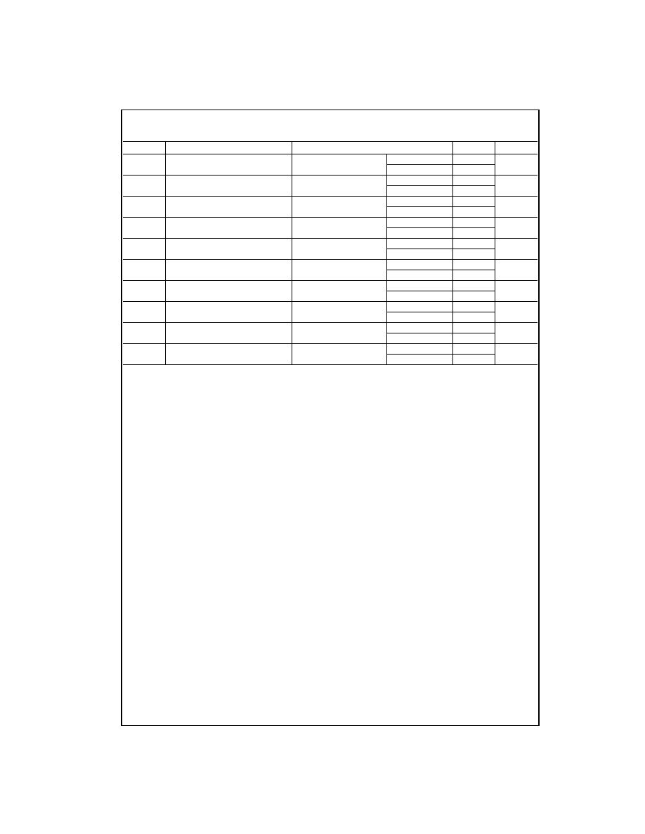
Absolute Maximum Ratings
(Note 1)
Note 1: The "Absolute Maximum Ratings" are those values beyond which
the safety of the device cannot be guaranteed. The device should not be
operated at these limits. The parametric values defined in the Electrical
Characteristics tables are not guaranteed at the absolute maximum ratings.
The "Recommended Operating Conditions" table will define the conditions
for actual device operation.
Recommended Operating Conditions
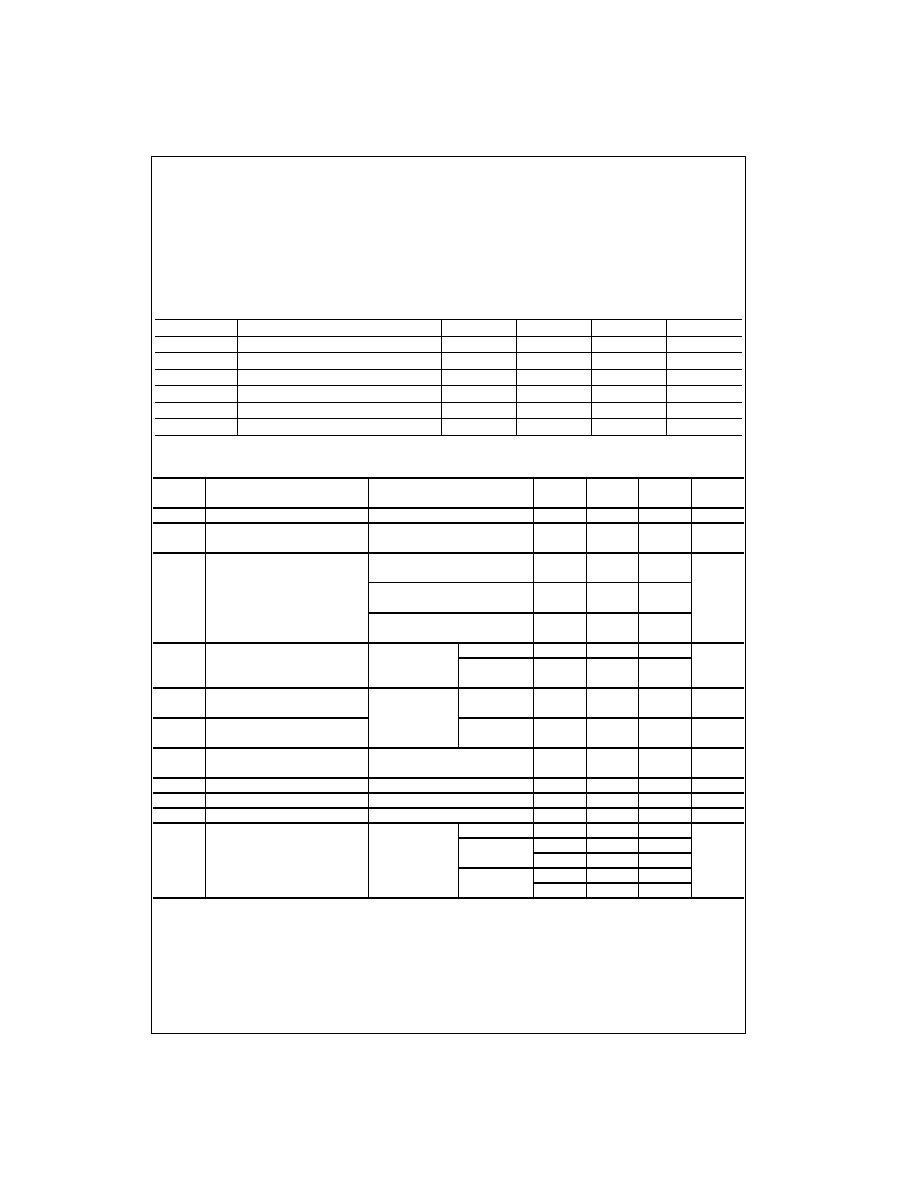
Electrical Characteristics
over recommended operating free air temperature range (unless otherwise noted)
Note 2: All typicals are at V
CC
=
5V, T
A
=
25
∞
C.
Note 3: Not more than one output should be shorted at a time, and the duration should not exceed one second.
Supply Voltage
7V
Input Voltage
7V
Operating Free Air Temperature Range
0
∞
C to
+
70
∞
C
Storage Temperature Range
-
65
∞
C to
+
150
∞
C
Symbol
Parameter
Min
Nom
Max
Units
V
CC
Supply Voltage
4.75
5
5.25
V
V
IH
HIGH Level Input Voltage
2
V
V
IL
LOW Level Input Voltage
0.8
V
I
OH
HIGH Level Output Current
-
15
mA
I
OL
LOW Level Output Current
24
mA
T
A
Free Air Operating Temperature
0
70
∞
C
Symbol
Parameter
Conditions Min
Typ
Max
Units
(Note 2)
V
I
Input Clamp Voltage
V
CC
=
Min, I
I
=
-
18 mA
-
1.5
V
HYS
Hysteresis (V
T
+
-
V
T
-
)
V
CC
=
Min
0.2
0.4
V
Data Inputs Only
V
OH
HIGH Level Output Voltage
V
CC
=
Min, V
IH
=
Min
2.7
V
IL
=
Max, I
OH
=
-
1 mA
V
CC
=
Min, V
IH
=
Min
2.4
3.4
V
V
IL
=
Max, I
OH
=
-
3 mA
V
CC
=
Min, V
IH
=
Min
2
V
IL
=
0.5V, I
OH
=
Max
V
OL
LOW Level Output Voltage
V
CC
=
Min
I
OL
=
12 mA
0.4
V
IL
=
Max
I
OL
=
Max
0.5
V
V
IH
=
Min
I
OZH
Off-State Output Current,
V
CC
=
Max
V
O
=
2.7V
20
µ
A
HIGH Level Voltage Applied
V
IL
=
Max
I
OZL
Off-State Output Current,
V
IH
=
Min
V
O
=
0.4V
-
20
µ
A
LOW Level Voltage Applied
I
I
Input Current at Maximum
V
CC
=
Max
0.1
mA
Input Voltage
V
I
=
7V
I
IH
HIGH Level Input Current
V
CC
=
Max, V
I
=
2.7V
20
µ
A
I
IL
LOW Level Input Current
V
CC
=
Max, V
I
=
0.4V
-
0.2
mA
I
OS
Short Circuit Output Current
V
CC
=
Max (Note 3)
-
40
-
225
mA
I
CC
Supply Current
V
CC
=
Max,
Outputs HIGH
13
23
Outputs OPEN
Outputs LOW
26
44
27
46
mA
Outputs Disabled
29
50
32
54
5
www.fairchildsemi.com
DM74LS240
∑ D
M
74LS24
1
Physical Dimensions
inches (millimeters) unless otherwise noted
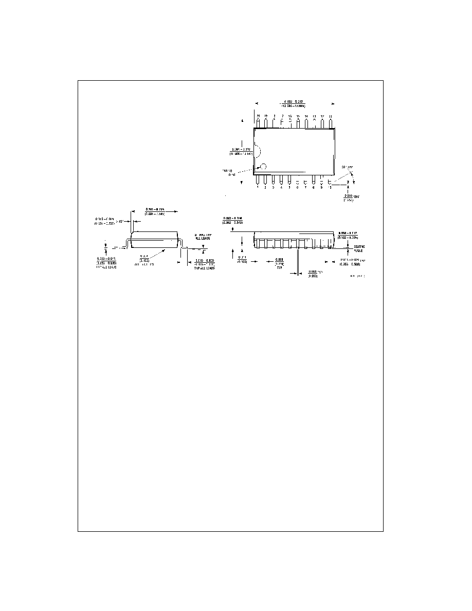
20-Lead Small Outline Integrated Circuit (SOIC), JEDEC MS-013, 0.300 Wide
Package Number M20B