 | –≠–ª–µ–∫—Ç—Ä–æ–Ω–Ω—ã–π –∫–æ–º–ø–æ–Ω–µ–Ω—Ç: BU-61xxx | –°–∫–∞—á–∞—Ç—å:  PDF PDF  ZIP ZIP |
Æ
Data Device Corporation
105 Wilbur Place
Bohemia, New York 11716
631-567-5600 Fax: 631-567-7358
www.ddc-web.com
FOR MORE INFORMATION CONTACT:
Technical Support:
1-800-DDC-5757 ext. 7771
FEATURES
∑
5 Volt Only
∑
Fully Integrated MIL-STD-1553 A/B
STANAG 3838 Compliant Terminals
∑
One-Square-Inch Package
∑
Smallest BC/RT/MT In The Industry
∑
Hardware and Software
Compatible with BU-61580 ACE
Series
∑
Flexible Processor/Memory
Interface
∑
Bootable RT* Option
∑
4K x 16 or 64K x 16* Shared RAM
∑
Automatic BC Retries
∑
Programmable BC Gap Times
∑
Programmable Illegalization
∑
Simultaneous RT/Monitor Mode
∑
Operates From 10*/12 /16 / 20* MHz
Clock
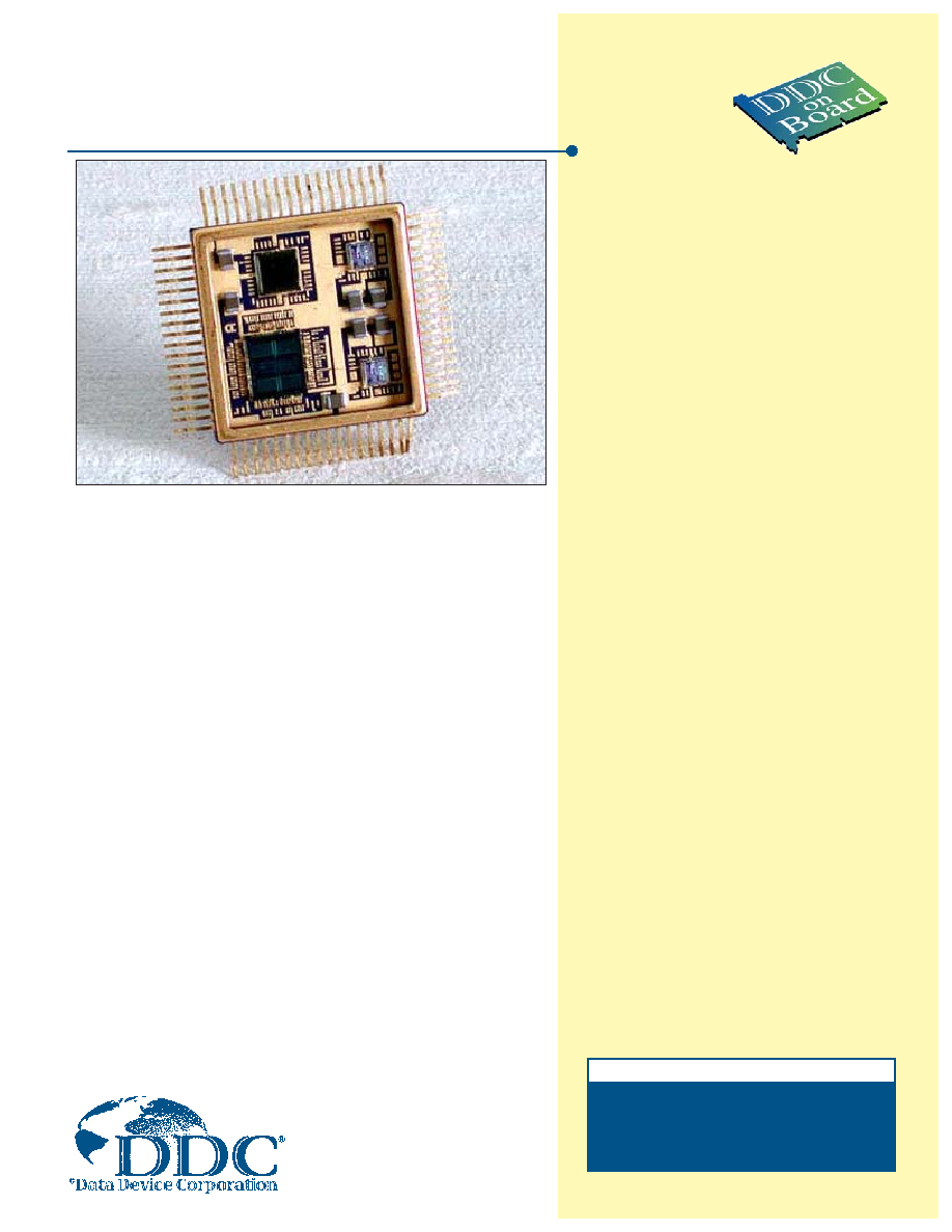
DESCRIPTION
The BU-61588 Mini-ACE and BU-61688 Mini-ACE Plus* integrates two
5-volt-only transceivers, protocol, memory management, processor interface
logic, and 4K x 16, or 64K x 16* words of RAM in a choice of pin grid array
(PGA), quad flat pack or gull lead packages. The Mini-ACE is packaged in a
1.0 square inch, low profile, cofired ceramic multi-chip-module (MCM) pack-
age making it the smallest integrated MIL-STD-1553 BC/RT/MT in the indus-
try.
The Mini-ACE provides full compatibility to DDC's BU-61580 and BU-65170
Advanced Communication Engine (ACE). As such, the Mini-ACE includes all
the hardware and software architectural features of the ACE.
The Mini-ACE contains internal address latches and bidirectional data buffers
to provide a direct interface to a host processor bus. The memory manage-
ment scheme for RT mode provides three data structures for buffering data.
These structures, combined with the Mini-ACE's extensive interrupt capabili-
ty, serve to ensure data consistency while off-loading the host processor.
The Mini-ACE Plus* can optionally boot-up as a RT with the Busy bit set for
1760 applications. The Mini-ACE BC mode implements several features
aimed at providing an efficient real-time software interface to the host proces-
sor including automatic retries, programmable intermessage gap times, auto-
matic frame repetition, and flexible interrupt generation.
The advanced architectural features of the Mini-ACE, combined with its small size
and high reliability, make it an ideal choice for demanding military and industrial
processor-to-1553 applications.
BU-65178/65179*/61588/61688*/61689*
MINIATURE ADVANCED
COMMUNICATION ENGINE
(MINI-ACE) AND MINI-ACE PLUS*
Make sure the next
Card you purchase
has...
©
1998, 1999 Data Device Corporation
All trademarks are the property of their respective owners.

2
Data Device Corporation
www.ddc-web.com
BU-65178/65179*/61688*/61689*
K-04/05-0
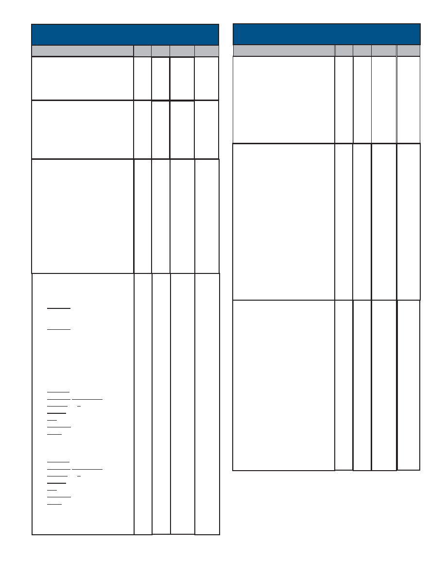
FIGURE 1.
B
U-65178/65179*/61588/61688*/61689*
TRANSCEIVER
A
CH. A
TRANSCEIVER
B
CH. B
DUAL
ENCODER/DECODER,
MULTIPROTOCOL
AND
MEMORY
MANAGEMENT
RT ADDRESS
4K X 16
OR
64K X 16
*
SHARED
RAM
ADDRESS BUS
PROCESSOR
AND
MEMORY
INTERFACE
LOGIC
DATA BUS
D15-D0
A15-A0
DATA
BUFFERS
ADDRESS
BUFFERS
PROCESSOR
DATA BUS
PROCESSOR
ADDRESS BUS
MISCELLANEOUS
CLK_IN,
MSTCLR,SSFLAG/EXT_TRG
RTAD4-RTAD0, RTADP
IOEN, READYD
ADDR_LAT/MEMOE, ZERO_WAIT/MEMWR,
8/16-BIT/DTREQ, POLARITY_SEL/DTACK
INT
TRANSPARENT/BUFFERED, STRBD, SELECT,
RD/WR, MEM/REG, TRIGGER_SEL/MEMENA-IN,
MSB/LSB/DTGRT
PROCESSOR
AND
MEMORY
CONTROL
INTERRUPT
REQUEST
TX/RX_A
TX/RX_A
TX/RX_B
TX/RX_B
RT_AD_LAT
3
Data Device Corporation
www.ddc-web.com
BU-65178/65179*/61688*/61689*
K-04/05-0
kohm
pF
Vp-p
Vpeak
5
0.860
10
2.5
0.20
0
V
V
V
6.0
7.0
Vcc+0.3
-0.3
-0.3
-0.3
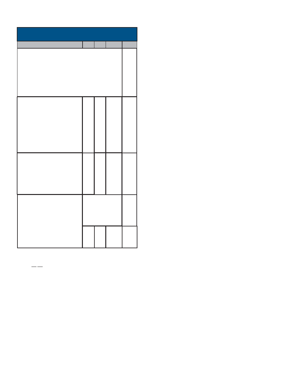
ABSOLUTE MAXIMUM RATING
Supply Voltage
Logic +5 V
Transceiver +5 V (Note 12)
Logic
Voltage Input Range
TABLE 1. BU-65178/65179*/61588/61688*/61689*
SPECIFICATIONS
UNITS
MAX
TYP
MIN
PARAMETER
RECEIVER
Differential Input Resistance
(Notes 1-7)
Differential Input Capacitance
(Notes 1-7)
Threshold Voltage, Transformer
Coupled, Measured on Stub
Common Mode Voltage (Note 7)
Vp-p
Vp-p
Vp-p
mVp-p,
diff
mV
nsec
9
27
27
10
250
300
7
21
22
150
6
18
20
-250
100
TRANSMITTER
Differential Output Voltage
Direct Coupled Across 35
,
Measured on Bus
Transformer Coupled Across
70
, Measured on Bus:
∑ Standard Product = ≠ XX0
∑ 1760 Amplitude Compliant
Product = ≠ XX2
( Note 13 and Ordering
Information ≠ Test Criteria)
Output Noise, Differential (Direct
Coupled)
Output Offset Voltage, Transformer
Coupled Across 70 ohms
Rise/Fall Time
V
V
µA
µA
µA
µA
µA
V
V
mA
mA
mA
mA
pF
pF
0.8
10
-84
-42
-100
-50
0.4
-6.4
-3.2
50
50
2.0
-10
-692
-346
-794
-397
2.4
6.4
3.2
LOGIC
VIH
VIL
IIH (Vcc = 5.5 V, VIN = Vcc)
IIH (Vcc = 5.5 V, VIN = 2.7 V)
SSFLAG/EXT_TRIG
All Other Inputs
IIL (Vcc = 5.5 V, VIN = 0.4 V)
SSFLAG/EXT_TRIG
All Other Inputs
VOH (Vcc = 4.5 V, VIH = 2.7 V,
VIL = 0.2 V, IOH = max)
VOL (Vcc = 4.5 V, VIH = 2.7 V,
VIL = 0.2 V, IOL = max)
IOL
DB15-DB0
A15-A0
MEMOE/ADDR_LAT
MEMWR/ZEROWAIT
DTREQ/16/8
DTACK/POLARITY_SEL
INT
READYD
IOEN
IOH
DB15-DB0
A15-A0
MEMOE/ADDR_LAT
MEMWR/ZEROWAIT
DTREQ/16/8
DTACK/POLARITY_SEL
INT
READYD
IOEN
CI (Input Capacitance)
CIO (Bi-directional signal input
capacitance)
TABLE 1. BU-65178/65179*/61588/61688*/61689*
SPECIFICATIONS (CONT.)
UNITS
MAX
TYP
MIN
PARAMETER
W
W
W
W
W
W
W
W
W
W
W
W
W
W
V
V
mA
mA
mA
mA
mA
mA
mA
mA
mA
mA
µs
µs
µs
µs
µs
µs
µs
µs
5.5
5.25
100
160
265
370
580
200
180
285
390
600
19.5
23.5
51.5
131
7
2.5
9.5
18.5
22.5
50.5
129.5
668
4.5
4.75
17.5
21.5
49.5
127
4
1553 MESSAGE TIMING
Completion of CPU Write (BC
Start)- to-Start of Next Message
BC Intermessage Gap (Note 8)
BC/RT/MT Response Timeout
(Note 9)
18.5 nominal
22.5 nominal
50.5 nominal
128.0 nominal
T Response Time (Note 11)
Transmitter Watchdog Timeout
0.115
0.64
0.93
1.22
1.81
0.230
0.64
0.93
1.22
1.80
0.18
0.42
0.66
1.14
0.5
0.88
1.11
1.33
1.97
1.0
0.99
1.22
1.45
1.90
0.28
0.51
0.75
1.22
POWER SUPPLY REQUIREMENTS
Voltages/Tolerances
BU-65178/61588X3
∑ +5 V (Logic)
∑ +5 V (Ch. A, Ch. B)
Current Drain (Total Hybrid)
BU-65178/65179/61588X0
∑ +5 V (Logic)
BU-65178/65179/61588X3
∑ +5 V (Logic, Ch. A, Ch. B)
∑ Idle
∑ 25% Transmitter Duty Cycle
∑ 50% Transmitter Duty Cycle
∑ 100% Transmitter Duty Cycle
BU-61688*/61689X0*
∑ +5 V (Logic)
BU-61688*/61689X3*
∑ +5 V (Logic, Ch. A, Ch. B)
∑ Idle
∑ 25% Transmitter Duty Cycle
∑ 50% Transmitter Duty Cycle
∑ 100% Transmitter Duty Cycle
5.0
5.0
23
116
222
328
540
46
116
217
318
519
POWER DISSIPATION
Total Hybrid
BU-65178/65179/61588X0
∑ +5 V (Logic)
BU-65178/61588/65179X3
∑ Idle
∑ 25% Duty Cycle
∑ 50% Duty Cycle
∑ 100% Duty Cycle
BU-61688*/61689X0*
∑ +5 V (Logic)
BU-61688*/61689X3*
∑ Idle
∑ 25% Duty Cycle
∑ 50% Duty Cycle
∑ 100% Duty Cycle
Hottest Die
BU-65178/61588X3/65179X3*/
BU-61688*/61689X3*
∑ Idle
∑ 25% Duty Cycle
∑ 50% Duty Cycle
∑ 100% Duty Cycle
* Mini-ACE PLUS with 64K Words of RAM. RAM impact to Power
Supply is based on Host Processor activity; subtract 140 mA if Host
is idle.
4
Data Device Corporation
www.ddc-web.com
BU-65178/65179*/61688*/61689*
K-04/05-0
TABLE 1. BU-65178/65179*/61588/61688*/61689*
SPECIFICATIONS (CONT.)
UNITS
MAX
TYP
MIN
PARAMETER
Frequency
BU-61588/61688*/65178
∑ Default Mode 16
∑ Software Programmable Option 12
BU-61689*
∑ Default Mode 20
∑ Software Programmable Option 10
BU-65179*
∑ Pin Programmable Option
10/12/16/20
MHz
MHz
MHz
MHz
MHz
Long Term Tolerance
∑ 1553A Mode
∑ 1553B Mode
Short Term Tolerance, 1 second
∑ 1553A Mode
∑ 1553B Mode
Duty Cycle
∑ 16 MHz
∑ 12 MHz
∑ 10 MHz*
∑ 20 MHz
%
%
%
%
%
%
%
%
0.01
0.1
0.001
0.01
67
60
60
60
33
40
40
40
THERMAL
Thermal Resistance, Junction-to-
Case, Hottest Die (
JC)
BU-65178/61588X3*
Operating Junction Temperature
Storage Temperature
Lead Temperature (soldering, 10
sec.)
∞C/W
∞C
∞C
∞C
6.8
150
150
+300
-55
-65
PHYSICAL CHARACTERISTICS
Size
BU-65178/61588 P
BU-65179*/61688*/61689*
BU-65178/61588 F/G
BU-65179*/61688*/61689*
Weight
BU-65178/61588 F/P/G
BU-65179*/61688*/61689*
in.
(mm)
in.
(mm)
0.3
(9)
1.0 X 1.0 X 0.150
(25.4 x 25.4 x 3.81)
1.0 X 1.0 X 0.155
(25.4 x 25.4 x 3.94)
oz
(g)
Notes: Notes 1 through 6 are applicable to the Receiver Differential
Resistance and Differential Capacitance specifications:
(1) Specifications include both transmitter and receiver (tied together internally).
(2) Measurement of impedance is directly between pins TX/RX A(B)
and TX/RX A(B) of the BU-65178/61588X3 hybrid.
(3) Assuming the connection of all power and ground inputs to the hybrid.
(4) The specifications are applicable for both unpowered and powered conditions.
(5) The specifications assume a 2 volt rms balanced, differential, sinu-
soidal input. The applicable frequency range is 75 kHz to 1 MHz.
(6) Minimum resistance and maximum capacitance parameters are
guaranteed, but not tested, over the operating range.
(7) Assumes a common mode voltage within the frequency range of dc to 2
MHz, applied to pins of the isolation transformer on the stub side (either direct
or transformer coupled), referenced to hybrid ground. Use a DDC recom-
mended transformer or other transformer that provides an equivalent CMRR.
Table 1 Notes (Cont.):
(8) Typical value for minimum intermessage gap time. Under software
control, may be lengthened to (65,535
µs minus message time), in
increments of 1
µs.
(9) Software programmable (4 options). Includes RT-to-RT Timeout (Mid-
Parity of Transmit Command to Mid-Sync of Transmitting RT Status).
(10) For both +5 V logic and transceiver. +5 V for channels A and B.
(11) Measured from mid-parity crossing of Command Word to mid-sync
crossing of RT's Status Word.
(12) External 10
µF Tantalum and 0.1 µF capacitors should be located
as close as possible to Pins 20 and 72 on the Flat Package
and Pins A9 and J3 on the PGA package, and 0.1
µF at Pin 37/D3.
(13) MIL-STD≠1760 requires that the Mini-ACE produce a 20 Vp-p min-
imum output on the stub connection.
5
Data Device Corporation
www.ddc-web.com
BU-65178/65179*/61688*/61689*
K-04/05-0
NOTES
** Note that the Test Output pins on the flat pack are pads located on
the bottom of the package.
1. BU-65179*, A15/A14 pins are actually CLK SEL 1 / CLK SEL 0 respectively.
2. BU-65179*, A12 pin selects the RT_BOOT_L OPTIONAL MODE.
3. BU-65179*, A13 pin has no connection.
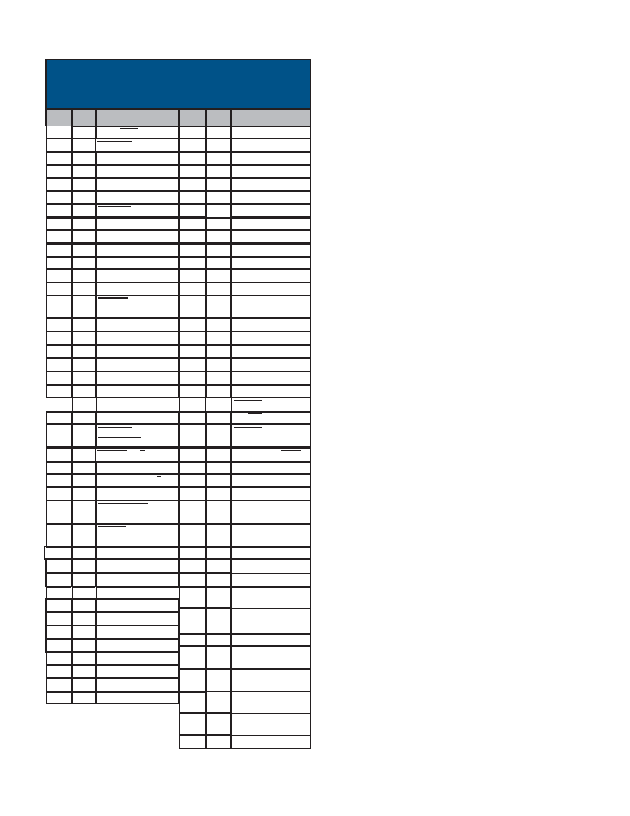
35
RTAD4
**
1
MEM/REG
42
D00
2
MSTCLR
43
D02
3
A11
44
D03
4
A10
45
D05
5
TX/RX-A
46
D08
6
A08
47
7
D07
TX/RX-A
48
8
D13
A14, See NOTE 1
49
D12
9
A04
50
D14
10
A03
51
D09
11
A07
52
D11
12
A02
53
D15
13
TX/RX-B
54
D10
14
MEMOE/ADDR_LAT
55
TRANSPARENT/
BUFFERED
15
A00
56
READYD
16
TX/RX-B
57
INT
17
LOGIC GND
58
IOEN
18
LOGIC GND
59
TX_INH_A
19
LOGIC GND
60
TX_INH_B
20
+5V V
CC2
61
SELECT
21
RTAD2
62
STRBD
22
A06
63
RD/WR
23
MEMWR/
ZEROWAIT
64
DTGRT/MSB/LSB
24
DTREQ/16/8
65
Test Output (RX-A)
25
Test Output (RX-B)
66
A15, See NOTE 1
26
Test Output (RX-B)
67
Test Output (RX-A)
27
A01
68
A05
28
MEMENA_IN/
TRIGGER_SEL
69
A09
29
DTACK/
POLARITY_SEL
70
A12, See NOTE 2
30
CLOCK_IN
71
A13, See NOTE 3
31
RT_AD_LAT
72
+5V V
CC1
32
SSFLAG/EXT_TRIG
**
TestOutput(A_RExt)
33
RTAD0
**
Test Output
(A_Test1)
34
RTAD3
**
Test Output
(AB_Test4)
TestOutput(B_RExt)
36
D06
**
TestOutput
(AB_Tstck)
H8
B4
B5
C2
C3
C1
D2
D1
C4
E3
F2
E1
F3
G1
G4
G3
H1
A7
A8
J8
A9
J7
F1
J2
H5
H3
H4
G2
J5
J6
H6
G7
H2
H7
G8
E8
E4
H9
F9
F7
G5
E7
E9
D7
B2
D9
B9
A2
D8
A1
C9
B8
C8
A3
B7
C7
C6
A6
A5
J1
A4
C5
B6
E2
J4
B3
B1
J3
D4
D5
D6
E6
37
D3
+5V V
CC
**
F4
TestOutput
(AB_Test2)
38
F8
D01
**
F5
TestOutput
(AB_Test3)
39
G6
D04
**
F6
TestOutput
(B_Test1)
40
G9
RTADP
N/A
E5
No Connect
41
J9
RTAD1
TABLE 2. BU-65178/65179*/61588/61688*/61689* PIN
LISTINGS (QFP QUAD FLAT PACK, PGA-PIN GRID
ARRAY AND GULL LEAD)
NAME
PGA
QFP
NAME
PGA
QFP
6
Data Device Corporation
www.ddc-web.com
BU-65178/65179*/61688*/61689*
K-04/05-0
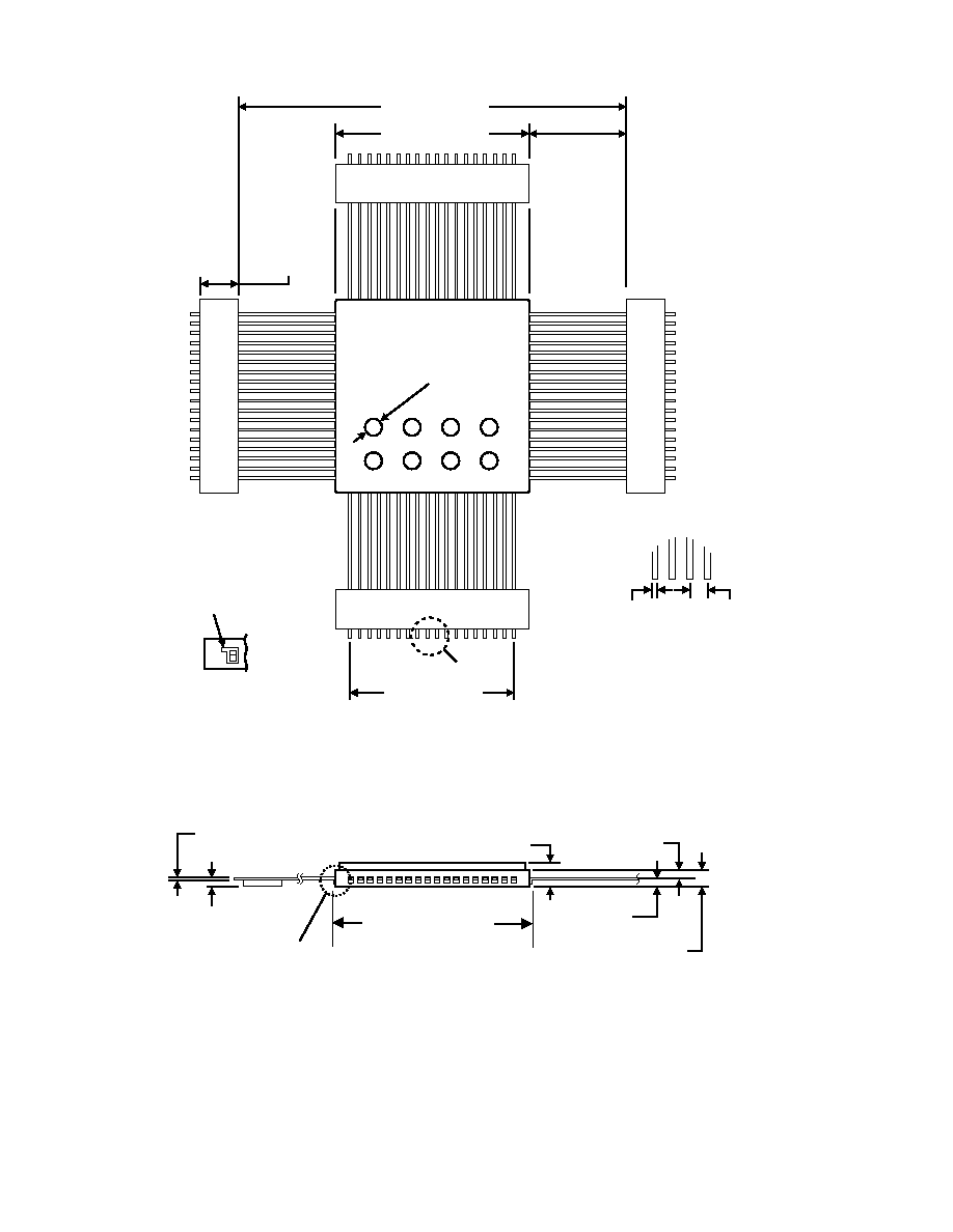
FIGURE 2. BU-65178F / 65179F* /61588F /61688F*/61689F* MECHANICAL OUTLINE (QUAD FLAT PACK - QFP)
1.000 SQ
±0.010
(25.400
±0.254)
72
1
VIEW "B"
0.018
±0.002
(0.457
±0.051)
0.050
±0.005
(1.270
±0.127)
Notes:
1) Dimensions are in inches (mm).
2) Package Material: Alumina (AL
2
O
3
)
3) Lead Material: Kovar, Plated by 50
µ in. minimum nickel under 60µ in. minimum gold.
4) There are 8 test pads located on the bottom of the package. These pads are recessed
so as not to interfere when mounting the hybrid.
VIEW "B"
2.000
±0.015
(50.800
±0.381)
0.500
±0.005
(12.70
±0.127)
0.200
±0.005
(5.080
±0.127)
0.850
±0.008
(21.590
±0.203)
0.010
±0.002
(0.254
±0.051)
0.035
±0.005
(0.889
±0.127)
0.040
±0.004
(1.016
±0.102)
0.050
±0.005
(1.270
±0.127)
0.090
±0.010
(2.286
±0.254)
0.130 MAX
(3.31)
BOTTOM VIEW
SIDE VIEW
VIEW "A"
VIEW "A"
INDEX DENOTES
PIN NO. 1
P4
P3
P2
P1
P8
P7
P6
P5
0.100 DIA.
(2.540) (see note 4)
1.024 ±0.014 NOM.
(26.010 ±0.356)
7
Data Device Corporation
www.ddc-web.com
BU-65178/65179*/61688*/61689*
K-04/05-0
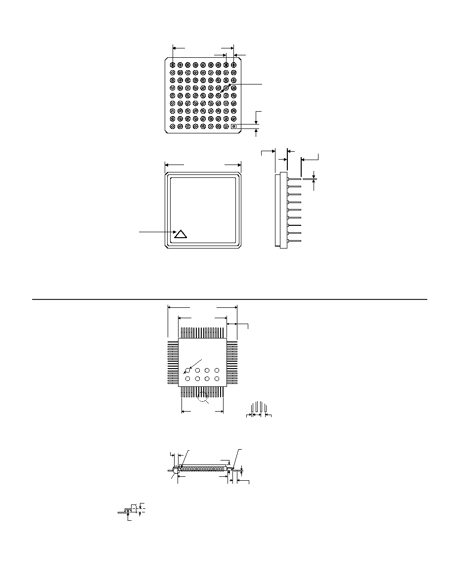
FIGURE 3. BU-65178P / 65179P* /61588P /61688P*/61689P* MECHANICAL OUTLINE (PIN GRID ARRAY - PGA)
FIGURE 4. BU-65178G / 65179G* /61588G /61688G*/61689G* MECHANICAL OUTLINE (GULL LEAD)
9
8
7
6
5
4
3
2
1
0.800 ±0.005
(20.320 ±0.127)
0.100 ±0.005
(2.540 ±0.127)
TOP VIEW
Notes:
1) Dimensions are in inches (mm).
2) Package Material: Alumina (AL
2
O
3
)
3) Lead Material: Kovar, Plated by 50
µ in. minimum nickel under 60µ in. minimum gold.
J H G F E D C B A
BOTTOM VIEW
1.000 SQ ±0.010
(25.400 ±0.254)
0.180 ±0.008
(4.572 ±0.203)
0.018 ±0.002
(0.457 ±0.051)
0.155 MAX
(3.810)
SIDE VIEW
0.070 ±0.005
(1.778 ±0.127)
0.070 ±0.005
(1.778 ±0.127)
Indicates
Pin A1
1.00 SQ
±0.01
(25.40
±0.25)
72
1
VIEW "B"
Notes:
1) Dimensions are in inches (mm).
2) Package Material: Alumina (AL
2
O
3
)
3) Lead Material: Kovar, Plated by 50
µ in. minimum nickel
under 60
µ in. minimum gold.
4) There are 8 test pads located on the bottom of the package.
These pads are recessed so as not to interfere when
mounting the hybrid.
VIEW "B"
1.38
±0.02
(35.05
±0.51)
0.19 Ref
(4.83 Ref)
0.850
±0.008
(21.590
±0.203)
0.08 MIN FLAT
(2.03)
0.130 MAX
(3.31)
0.018
±0.002
(0.457
±0.051)
0.050
±0.005
(1.270
±0.127)
BOTTOM VIEW
SIDE VIEW
VIEW "A"
INDEX DENOTES
PIN NO. 1
P4
P3
P2
P1
P8
P7
P6
P5
0.100 DIA.
(2.540) (see note 4)
0.010
±0.002
(0.254
±0.051)
0.012 R. MAX
(0.305 R.)
0.05 MIN FLAT
(1.27)
0.075 MAX FLAT
(1.91)
1.024 ±0.014 NOM.
(26.010 ±0.356)
VIEW "A"
0.006 -0.004,+0.010
(0.152
-0.100,+ 0.254)
0.050 ±0.005
(1.27 ±0.127)

8
Data Device Corporation
www.ddc-web.com
BU-65178/65179*/61688*/61689*
K-04/05-0
TRANSFORMERS
In selecting isolation transformers to be used with the Mini-ACE,
there is a limitation on the maximum amount of leakage induc-
tance. If this limit is exceeded, the transmitter rise and fall times
may increase, possibly causing the bus amplitude to fall below
the minimum level required by MIL-STD-1553. In addition, an
excessive leakage imbalance may result in a transformer dynam-
ic offset that exceeds 1553 specifications.
The maximum allowable leakage inductance is 6.0 µH, and
is measured as follows:
The side of the transformer that connects to the
Mini-ACE is defined as the "primary" winding. If one side of the
primary is shorted to the primary center-tap, the inductance
should be measured across the "secondary" (stub side) winding.
This inductance must be less than 6.0 µH. Similarly, if the other
side of the primary is shorted to the primary center-tap, the
inductance measured across the "secondary" (stub side) wind-
ing must also be less than 6.0 µH.
The difference between these two measurements is the
"differential" leakage inductance. This value must be less than
1.0 µH.
Beta Transformer Technology Corporation (BTTC), a subsidiary
of DDC, manufactures transformers in a variety of mechanical
configurations with the required turns ratios of 1:2.5 direct cou-
pled, and 1:1.79 transformer coupled. TABLE 3 provides a listing
of many of these transformers. For further information, contact
BTTC at 631-244-7393 or at www.bttc-beta.com.
DLP-7014
SLP-8007
SLP-8024
NOT RECOMMENDED
LPB-5015
TLP-1005
HLP-6015
Dual epoxy transformer, side by side, surface mount, 0.930" X 0.630", 0.155" max height
DLP-7115 (see note1)
Dual epoxy transformer, side by side, surface mount, 1.410" X 0.750", 0.130" max height
Single metal transformer, hermetically sealed, surface mount, 0.630" X 0.630", 0.175" max height
TLP-1105
HLP-6014
Dual epoxy transformer, side by side, flat pack, 0.930" X 0.630", 0.155" max height
Single metal transformer, hermetically sealed, flat pack, 0.630" X 0.630", 0.175" max height
TLP-1205
Dual epoxy transformer, side by side, through-hole, 0.930" X 0.630", 0.155" max height
TST-9027
Dual epoxy transformer, twin stacked, flat pack, 0.625" X 0.625", 0.280" max height
TST-9017
Dual epoxy transformer, twin stacked, surface mount, 0.625" X 0.625", 0.280" max height
TST-9007
Dual epoxy transformer, twin stacked, 0.625" X 0.625", 0.280" max height
B-3819
LPB-5014
Single epoxy transformer, surface mount, hi-temp solder, 0.625" X 0.625", 0.220" max height.
Single epoxy transformer, flat pack, 0.625" X 0.625", 0.150" max height
B-3227
Single epoxy transformer, surface mount, 0.625" X 0.625", 0.275" max height
B-3231
Single epoxy transformer, flat pack, 0.625" X 0.625", 0.275" max height
B-3818
B-3067
B-3226
Single epoxy transformer, through-hole, 0.625" X 0.625", 0.220" max height.
Single epoxy transformer, through-hole, 0.625" X 0.625", 0.250" max height
BTTC PART NO.
TRANSFORMER CONFIGURATION
Single epoxy transformer, surface mount, 0.625" X 0.625", 0.150" max height
B-3229
Single epoxy transformer, through hole, transformer coupled only, 0.500" X 0.350", 0.250" max height
TABLE 3. BTTC TRANSFORMERS FOR USE WITH MINI-ACE
Notes:
1. DLP-7115 operates to +85∞C max. All other transformers listed operate to +130∞C max.
9
Data Device Corporation
www.ddc-web.com
BU-65178/65179*/61688*/61689*
K-04/05-0
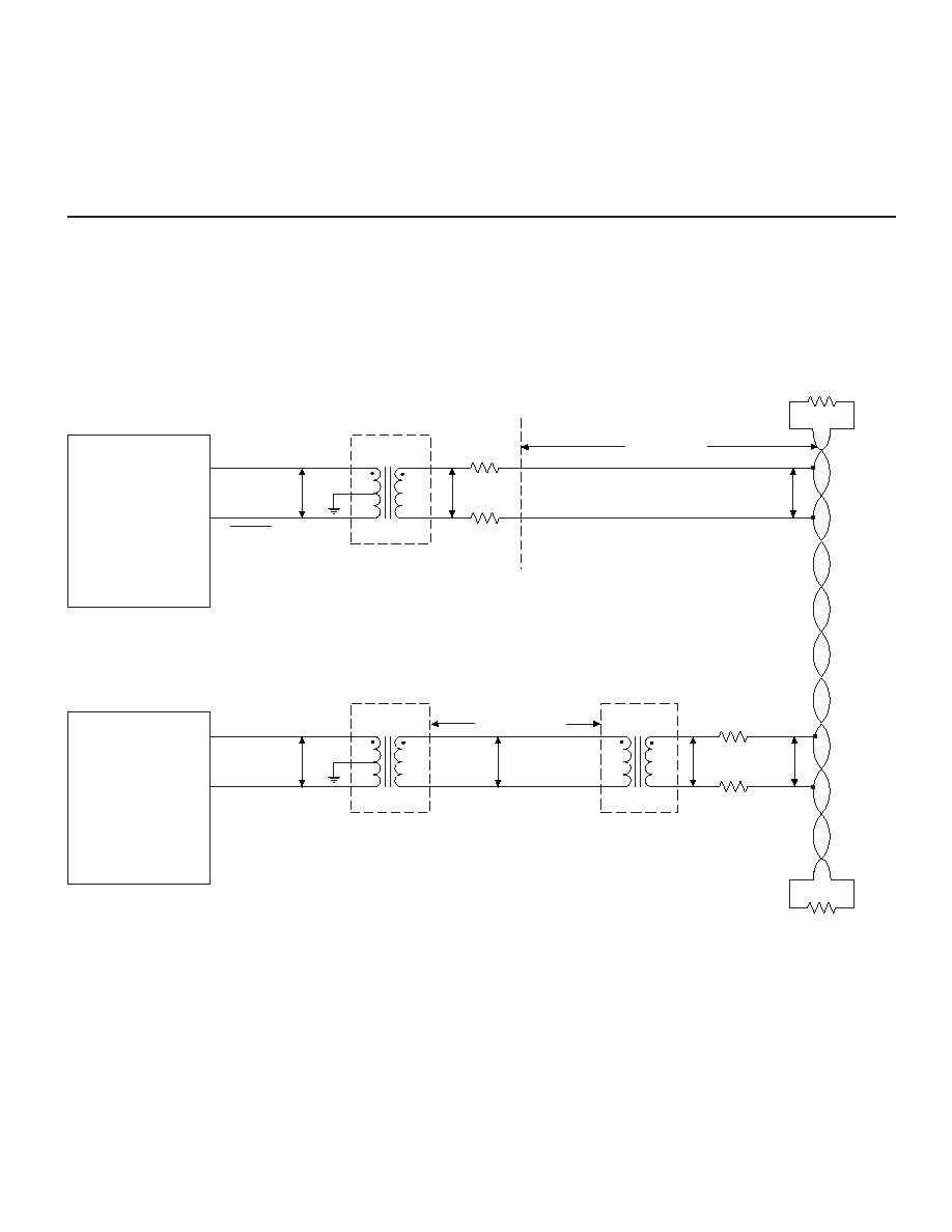
INTERFACE TO MIL-STD-1553 BUS
FIGURE 5 illustrates the interface between the various versions
of the Mini-ACE and a MIL-STD-1553 bus. Connections for both
direct (short stub) and transformer (long stub) coupling, as well
as the nominal peak-to-peak voltage levels at various points
(when transmitting), are indicated in the diagram.
Mini-ACE
DATA
BUS
Z
0
55
55
TX/RX
TX/RX
(1:2.5)
11.2 Vpp
28 Vpp
1 FT MAX
Z
0
(1:1.79)
11.2 Vpp
20 Vpp
(1:1.41)
COUPLING
TRANSFORMER
0.75 Z
0
0.75 Z
0
LONG STUB
(TRANSFORMER
COUPLED)
20 FT MAX
28 Vpp
SHORT STUB
(DIRECT COUPLED)
OR
NOTES: 1. Z
0
= 70 TO 85 OHMS
ISOLATION
TRANSFORMER
ISOLATION
TRANSFORMER
7 Vpp
7 Vpp
2. NOMINAL VOLTAGE
LEVELS SHOWN
Mini-ACE
FIGURE 5. MINIATURE ADVANCED COMMUNICATIONS ENGINE INTERFACE TO MIL-STD-1553 BUS
10
Data Device Corporation
www.ddc-web.com
BU-65178/65179*/61688*/61689*
K-04/05-0
ORDERING INFORMATION
BU-61588F3-11XX
Supplemental Process Requirements:
S = Pre-Cap Source Inspection
L = Pull Test
Q = Pull Test and Pre-Cap Source Inspection
K = One Lot Date Code
W = One Lot Date Code and Pre-Cap Source Inspection
Y = One Lot Date Code and 100% Pull Test
Z = One Lot Date Code, Pre-Cap Source Inspection and 100% Pull Test
Blank = None of the Above
Test Criteria:
0 = Standard Testing
2 = MIL-STD-1760 Amplitude Compliant - Applies to +5 Volt Transceiver Option Only
Process Requirements:
0 = Standard DDC processing, no Burn-In (See table on next page)
1 = MIL-PRF-38534 Compliant
2 = B*
3 = MIL-PRF-38534 Compliant with PIND Testing
4 = MIL-PRF-38534 Compliant with Solder Dip
5 = MIL-PRF-38534 Compliant with PIND Testing and Solder Dip
6 = B* with PIND Testing
7 = B* with Solder Dip
8 = B* with PIND Testing and Solder Dip
9 = Standard DDC Processing with Solder Dip, no Burn-In (See table on next page)
Temperature Range/Data Requirements:
1 = -55∞C to +125∞C
2 = -40∞C to +85∞C
3 = 0∞C to +70∞C
4 = -55∞C to +125∞C with Variables Test Data
5 = -40∞C to +85∞C with Variables Test Data
8 = 0∞C to +70∞C with Variables Test Data
Voltage/Transceiver Option:
0 = No Transceivers
3 = +5 Volts, rise/fall times=100 to 300 ns (-1553B) (See Test Criteria - 1760 Compliant with option -XX2)
Package Type:
F = 72-Pin Quad Flat Pack
P = 81-Pin PGA
G = 72-Pin Gull Lead (Contact factory.)
Product Type:
65178 = RT Only, 16/12 MHz, 4K RAM
61588 = BC/RT/MT, 16/12 MHz, 4K RAM
65179 = RT/RT_BOOT, 10/12/16/20 MHz, 4K RAM
61688 = BC/RT/MT, 12/16 MHz, 64K RAM
61689 = BC/RT/MT, 10/20 MHz, 64K RAM
*Standard DDC Processing with burn-in and full temperature test, see table on next page.

11
Data Device Corporation
www.ddc-web.com
BU-65178/65179*/61688*/61689*
K-04/05-0
TABLE 1
1015
(note 1)
, 1030
(note 2)
BURN-IN
Notes:
1. For Process Requirement "B*" (refer to ordering information), devices may be non-compliant with MIL-
STD-883, Test Method 1015, Paragraph 3.2. Contact factory for details.
2. When applicable.
3000g
2001
CONSTANT ACCELERATION
C
1010
TEMPERATURE CYCLE
A and C
1014
SEAL
--
2009, 2010, 2017, and 2032
INSPECTION
CONDITION(S)
METHOD(S)
MIL-STD-883
TEST
STANDARD DDC PROCESSING
FOR HYBRID AND MONOLITHIC HERMETIC PRODUCTS

12
K-04/05-0
PRINTED IN THE U.S.A.
The information in this data sheet is believed to be accurate; however, no responsibility is
assumed by Data Device Corporation for its use, and no license or rights are
granted by implication or otherwise in connection therewith.
Specifications are subject to change without notice.
Please visit our Web site at www.ddc-web.com for the latest information.
105 Wilbur Place, Bohemia, New York, U.S.A. 11716-2482
For Technical Support - 1-800-DDC-5757 ext. 7771
Headquarters, N.Y., U.S.A. - Tel: (631) 567-5600, Fax: (631) 567-7358
Southeast, U.S.A. - Tel: (703) 450-7900, Fax: (703) 450-6610
West Coast, U.S.A. - Tel: (714) 895-9777, Fax: (714) 895-4988
United Kingdom - Tel: +44-(0)1635-811140, Fax: +44-(0)1635-32264
Ireland - Tel: +353-21-341065, Fax: +353-21-341568
France - Tel: +33-(0)1-41-16-3424, Fax: +33-(0)1-41-16-3425
Germany - Tel: +49-(0)89-15 00 12-11, Fax: +49-(0)89-15 00 12-22
Japan - Tel: +81-(0)3-3814-7688, Fax: +81-(0)3-3814-7689
World Wide Web - http://www.ddc-web.com
DATA DEVICE CORPORATION
REGISTERED TO ISO 9001:2000
FILE NO. A5976
R
E
G
IS
T ERED
FI
R
M
Æ
U