 | ÐлекÑÑоннÑй компоненÑ: B4251CR | СкаÑаÑÑ:  PDF PDF  ZIP ZIP |
Äîêóìåíòàöèÿ è îïèñàíèÿ www.docs.chipfind.ru
Bay Linear, Inc
2478 Armstrong Street, Livermore, CA 94550 Tel: (925) 606-5950, Fax: (925) 940-9556 www.baylinear.com
250mA Low Dropout Voltage Regulators
B4251
ON/OFF & BYPASS
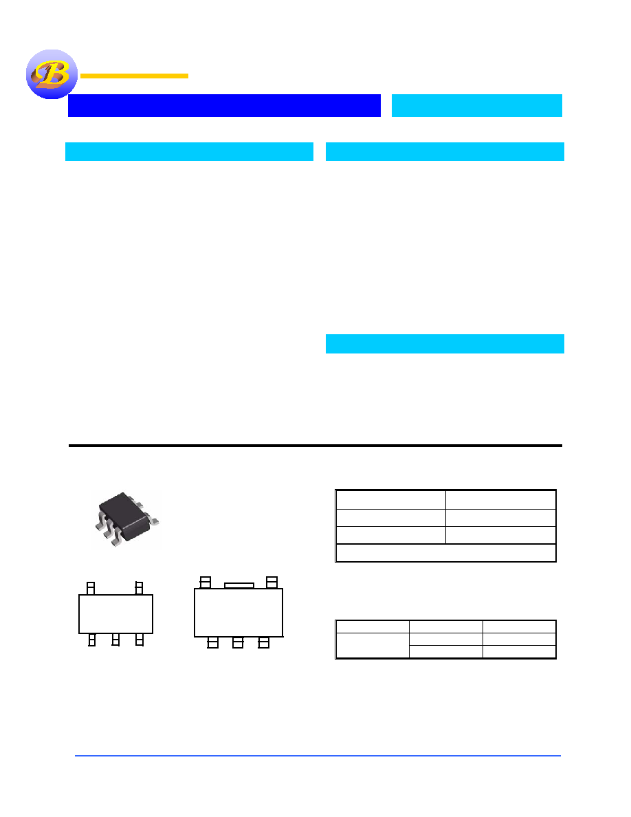
Pin Connection
Ordering Information
Package Part
No.
SOT-25 B4251CK5-X.X
SOT-89 B4251CR-X.X
X.X = Fixed Output Voltages from 2.0V to 6.0V
ON/OFF (Enable) Function
Part No
ON/Off
V
OUT
High ON
B4251
Low OFF
Description
The B4251 series are a group of positive output voltage,
five-pin regulators, which provide a high current even
when the input/output voltage differential is small. Low
power consumption and high accuracy is achieved
though CMOS and programmable fuse technologies.
Output voltage: 2.0V to 6.0V in 0.1V increments.
The B4251 consists of a high-precision voltage
reference, an error correction circuit, and a current
limited output driver. Key features include a Shutdown
Pin that reduces supply current to 0.5
µA max and a
470pF Bypass input to ground reduces noise present on
the internal reference, which in turn significantly reduce
output noise. If output noise is not concern, this input
maybe left unconnected. Larger capacitor values cap be
used, but results in longer time period to rated output
voltage when power initially applied.
The ON/OFF pin enables the output to be turned off,
resulting in reduced power consumption. Provided in
SOT-25 (150mW) packages minimizes the usage of
board real state.
Features
· Maximum Output Current: 250 mA.
· Highly Accurate Output Voltage +/- 1.4%
· Only 19µA Power Consumption MAX
· Shutdown Supply Current 1µA
· Ground Current of Less than 5µA
· Very Low Dropout
0.12V at 100mA
0.23V at 250mA
· Shutdown Mode for Power Savings
· With ON/OFF & BYPASS Features
· Offered in SOT-89 & SOT-25 Packages
· PIN-to-PIN S-818
Applications
· Battery Powered Equipment
· Notebook PC, Palmtops, PDA
· Portable Cameras and Video Recorders
· Reference Voltage Sources
· Cellular / GSM / PCS Phones
Bay Linear
Inspire the Linear Power
SOT-89 (R)
Top View
On/Off
V
in
Vss
3
2
1
4
5
V
out
NC
SOT-25 (K5)
Top View
ON/OFF
V
in
GND
3
2
1
4
5
V
out
Bypass
Bay Linear, Inc
2478 Armstrong Street, Livermore, CA 94550 Tel: (925) 606-5950, Fax: (925) 940-9556 www.baylinear.com
B4251
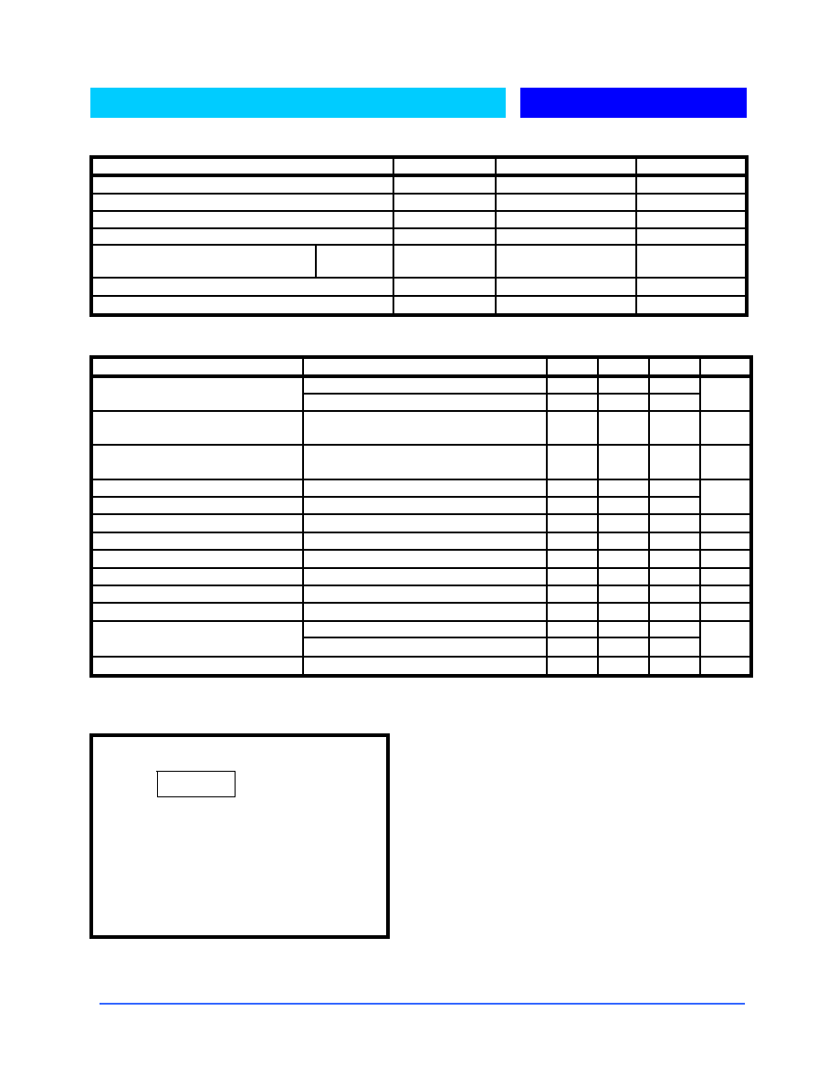
Absolute Maximum Ratings
Parameter Symbol
Ratings
Units
Input Voltage
V
IN
12 V
Output Current
I
OUT
500
mA
Output Voltage
V
OUT
V
SS
-0.3 to V
IN
0.3
V
On/Off Voltage
On/Off
V
SS
-0.3 to V
IN+
0.3
V
Continual Total Power Dissipation
SOT-25
SOT-89
Pd
150
300
mW
Operating Ambient Temperature
T
OPR
-30 to 80
°C
Storage Temperature
T
STG
-40 to 125
°C
Electrical Characteristics (T
a
= 25
°C, V
IN
= V
OUT +
0.5V; unless otherwise noted)
Parameter Conditions
MIN
TYP
MAX
UNIT
I
O
= 1mA
-1.4%
-
+1.4%
Output Voltage Accuracy
I
O
= 0 to 150mA
-2%
-
+2%
V
Line Regulation
V
OUT
/
V
IN
-V
OUT
I
O
= 100mA,
(V
OUT
+ 0.1V)<V
IN
<6V
0.2 0.3 %/V
Load Regulation
VIN 6V, 0mA < I
O
< 120mA C
OUT
= 1
µF
0.01
0.04 %/mV
Maximum Output Current
250
Current Limit
160
500
mA
Shutdown Supply Current
T
A
=25
°C
0.01 1
µA
Shutdown Input Bias Current
VSHDN=V
IN,
T
A
=25
°C
0.01
100 nA
Shutdown Exit Delay
CBP=0
µF C
OUT
=1
µF, I
O
= 1mA
30
150
µsec
Shutdown Input Threshold Low
V
in
=2.5 to 5.5V
0.4
V
Shutdown Input Threshold High
V
in
=2.5 to 5.5V
2
V
Ground Pin Current
I
OUT
= 0mA......150mA
2 5
µA
I
O
= 150mA
160
250
Dropout Voltage
I
O
= 250 mA
200
280
mV
Thermal Shutdown Temperature
155
°C
Marking Format
SOT-25
FXWW
F = B4251
Variables
X = Voltage Codes
WW = Work Week Code
B = 2.0
F = 3.3
SOT-25 = 01 to 99
C = 2.5
G = 3.5
D = 2.8
H = 5.0
E = 3.0

Bay Linear, Inc
2478 Armstrong Street, Livermore, CA 94550 Tel: (925) 606-5950, Fax: (925) 940-9556 www.baylinear.com
B4251
PRODUCT DESCRIPTION
The B4251 is precision fixed output voltage regulator.
Unlike bipolar regulators, the B4251 supply current
does not increase with load current. In addition, V
out
remains stable and within regulator at very low load
currents (an important consideration in RTC and
CMOS RAM battery back-up application).
Figure 1 shows a typical application circuit. The
regulator is enabled any time the shutdown input is at
or above V
IH.
And shutdown (disabled) when SHDN is
at or below V
IL
. SHDN maybe controlled by a CMOS
logic gate, or I/O port of a micro controller. If the
SHDN input is not. Required, it should be connected
directly to the supply. While in shutdown, supply
current decreases to 0.05
µA (typical) and V
out
falls to
zero volts.
Bypass Input
A 470pF capacitor connected from the bypass input to
ground reduces noise present on the internal reference,
which in turn significantly reduces output noise. If
output noise is not a concern, this input maybe left
unconnected. Larger capacitor values maybe used, but
it results in a longer time period to rated output
voltage power is initially applied.
Output Capacitor
A 1
µF (min) capacitor from V
out
to ground is required.
Then output capacitor should have an effective series
resistance of 5
or less. A 1µA capacitor should be
connected from V
in
to GND if there is more than 10
inches of wire between the regulator and the AC filter
capacitor, or if a battery is used as the power source.
Aluminum electrolytic or tantalum capacitor types can
be used. (since many aluminum electrolytic capacitors
freeze at approximately- 30
°C, solid tantalums are
recommended for applications operating below 25
°C.) When operating from sources other than
batteries, supply-noise rejection and transient response
can be improved by increasing the value of the input
and output capacitors and employing passive filtering
techniques.
Thermal Considerations
Thermal Shutdown
Integrated thermal protection circuitry shuts the
regulator off when die temperature exceeds 160
°C.
The regulator remaining off until the die temperature
drops to approximately 150
°C.
Power Dissipation
The amount of power the regulator dissipates is
primarily a function of input and output voltage, and
output current. The following equation is used to
calculate worst case power dissipation:
P
D
=(V
INMAX
-V
OUTMIN
)I
LOADMAX
Where:
P
D
= worst case actual power dissipation
V
INMAX
= Maximum voltage on V
IN
V
OUTMIN
=Minimum regulator output voltage
I
LOADMAX
= maximum output (LOAD) Current
The maximum allowable power dissipation is function
of the maximum ambient temperature (T
AMAX
). The
maximum allowable die temperature (125
°C) and the
thermal resistance from junction-to-air (
JA
). The 5-
pin SOT-23A package has a
JA
of approximately
220
°C/Watt when mounted on a single layer FR4
dielectric copper clad PC board.
P
DMAX
=(T
JMAX
-T
AMAX
)/
JA
Where all terms are previously defined
This can be caused in conjunction with other equation
to ensure regulator thermal operation is within limit.
For example:
Given:
V
INMAX
=3.0V+10%
V
OUTMIN
=2.7V-2.5%
I
LOADMAX
=40 mA
T
JMAX
=125
°C
T
AMAX
=55
°C
Find:
1. Actual power dissipation
2. Maximum allowable dissipation
Actual power dissipation:
P
D
=(V
INMAX
-V
OUTMIN
)I
LOADMAX
=[(3.0 x 1.1)-(2.7 x 0.975)]40 x 10
-3
=26.7mW
Maximum allowable power dissipation:
P
DMAX
=(T
JMAX
-T
AMAX
)
=(125-55)/220
=318Mw
These equations can be used to calculate maximum
current and/or input voltage limits.
Bay Linear, Inc
2478 Armstrong Street, Livermore, CA 94550 Tel: (925) 606-5950, Fax: (925) 940-9556 www.baylinear.com
B4251
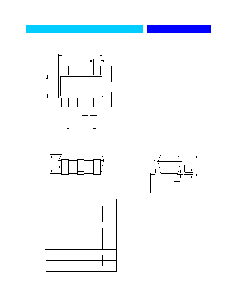
SOT-25 Packaging Outline
L
A1
C
A2
A
D
B (5 PLACES)
H
E
e1
e
MILLIMETERS
SYMBOL
0
0.90
0.30
0.80 REF
2.70
0.10
1.40
1.70
0.95 BSC.
MIN 0.2
2.50
MIN.
MAX
MIN.
MAX.
A
A1
A2
B
C
D
E
e
e1
H
L
0
.035
.012
.0315 REF
.106
.004
.055
.066
.037 BSC.
MIN .0078
.098
0.10
1.30
0.50
3.10
0.35
1.80
2.10
3.00
.004
.051
.019
.122
.0137
.071
.082
.118
INCHES
NOTE:
1. REFER TO APPLICABLE
2. CONTROLLING DIMENTION : MILLIMETER
3. PACKAGE SURFACE FINISHING TO BE SMOOTH
FINISH.

Bay Linear, Inc
2478 Armstrong Street, Livermore, CA 94550 Tel: (925) 606-5950, Fax: (925) 940-9556 www.baylinear.com
Advance Information- These data sheets contain descriptions of products that are in development. The specifications are based on the engineering calculations,
computer simulations and/ or initial prototype evaluation.
Preliminary Information- These data sheets contain minimum and maximum specifications that are based on the initial device characterizations. These limits are
subject to change upon the completion of the full characterization over the specified temperature and supply voltage ranges.
The application circuit examples are only to explain the representative applications of the devices and are not intended to guarantee any circuit
design or permit any industrial property right to other rights to execute. Bay Linear takes no responsibility for any problems related to any
industrial property right resulting from the use of the contents shown in the data book. Typical parameters can and do vary in different
applications. Customer's technical experts must validate all operating parameters including " Typical" for each customer application.
LIFE SUPPORT AND NUCLEAR POLICY
Bay Linear products are not authorized for and should not be used within life support systems which are intended for surgical
implants into the body to support or sustain life, in aircraft, space equipment, submarine, or nuclear facility applications without
the specific written consent of Bay Linear President.