KSD-O2B011-001
1
SM3317-D / SM3317-D(B)
High Brightness LED Lamp
2
1
2
1
2.80~3.20
2 . 7 0 ~ 3 . 1 0
5 . 1 0 ~ 5 . 5 0
2 3 . 0 0 M i n .
0 . 7 0 M a x .
1 . 0 0 M i n .
2 . 5 4 T y p .
3 . 5 0 ~ 3 . 9 0
3 . 6 0 ~ 4 . 0 0
0
.
4
5
M
a
x
.
2.80~3.20
2 . 7 0 ~ 3 . 1 0
5 . 1 0 ~ 5 . 5 0
4 . 7 0 ~ 5 . 7 0
2 3 . 0 0 M i n .
1 . 0 0 M i n .
2 . 5 4 T y p .
3 . 5 0 ~ 3 . 9 0
3 . 6 0 ~ 4 . 0 0
0
.
4
5
M
a
x
.
1 . 2 0 M i n .
0 . 7 0 M a x .
1
.
2
7
T
y
p
.
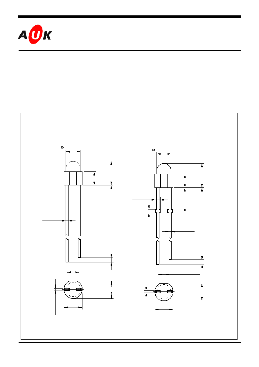
Features
· 3mm(T-1) all plastic mold type
· Available on tape and reel
Outline Dimensions unit :
mm
STRAIGHT TYPE STOPPER TYPE : (B)
PIN Connections
1. Anode
2. Cathode
S
S
e
e
m
m
i
i
c
c
o
o
n
n
d
d
u
u
c
c
t
t
o
o
r
r
KSD-O2B011-001
2
SM3317-D / SM3317-D(B)
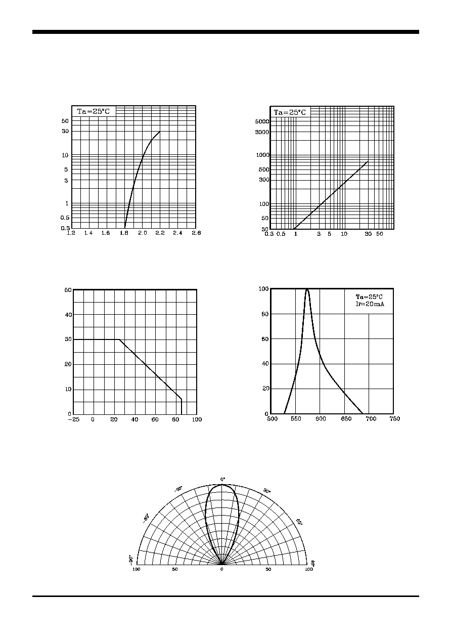
Absolute Maximum Ratings
(Ta=25)
Characteristic Symbol
Rating
Unit
Power dissipation
P
D
70
mW
Forward current
I
F
30
mA
*
1
Peak forward current
I
FP
50 mA
Reverse voltage
V
R
4 V
Operating temperature range
T
opr
-2585
Storage temperature range
T
stg
-30100
*
2
Soldering temperature
T
sol
260 for 10 seconds
*1.Duty ratio = 1/16, Pulse width = 0.1ms
*2.Keep the distance more than 2.0mm from PCB to the bottom of LED package
Electrical / Optical Characteristics
(Ta=25)
Characteristic Symbol
Test
Condition
Min
Typ
Max
Unit
Forward voltage
V
F
I
F
= 20mA
1.9
-
2.3
V
*
4
Luminous intensity
I
V
I
F
= 20mA
230
-
780
mcd
Dominant wavelength
D
I
F
= 20mA
569
572
575
nm
Spectrum bandwidth
I
F
=
20mA
- 30 - nm
Reverse current
I
R
V
R
=4V -
-
10
uA
*
3
Half angle
1/2
I
F
= 20mA
-
±22
- deg
*3.
1/2
is the off-axis angle where the luminous intensity is 1/2 the peak intensity
*4. Luminous intensity maximum tolerance for each grade classification limit is ±18%
V
F
/ I
V
/
D
Grade Classification (Ta=25)
Test Condition @I
F
= 20mA
Forward Voltage [V]
Luminous Intensity [mcd]
Dominant Wavelength [nm]
a : 569~571
N : 230~350
1 : 1.9~2.1
b
1
: 571~572
O : 350~520
b
2
: 572~573
2 : 2.1~2.3
P : 520~780
c : 573~575
(Do not use to combine grade classification. It must be used separately grade classification)
KSD-O2B011-001
4
SM3317-D / SM3317-D(B)
The AUK Corp. products are intended for the use as components in general electronic
equipment (Office and communication equipment, measuring equipment, home
appliance, etc.).
Please make sure that you consult with us before you use these AUK Corp. products
in equipments which require high quality and / or reliability, and in equipments which
could have major impact to the welfare of human life(atomic energy control, airplane,
spaceship, transportation, combustion control, all types of safety device, etc.). AUK
Corp. cannot accept liability to any damage which may occur in case these AUK Corp.
products were used in the mentioned equipments without prior consultation with AUK
Corp..
Specifications mentioned in this publication are subject to change without notice.