KSI-W025-001
1
SL2055
PREAMPLIFIER FOR REMOTE CONTROL USE
Description
· The SL 2055 is bipolar IC for receiving preamplifier of infrared remote control system. It
consists of a head amplifier, a limiter, a band pass filter, a signal waveform detector, and a
waveform rectifier, etc.
Features
· Built-in filter enable to vary center frequency by an external resistance
(fo=30KHz to 80KHz, 38KHz typ.)
· Possible to direct connection to a photo diode.
· Open collector output(directly connectable to TTL and CMOS)
· Internal pull-up resistance and power filter resistance(low-capacitance)
· Less chances of malfunction associated with a high frequency lighting floure internal trap
circuit
Ordering
Information
Type NO.
Marking
Package Code
SL2055
SL2055
SOP-8
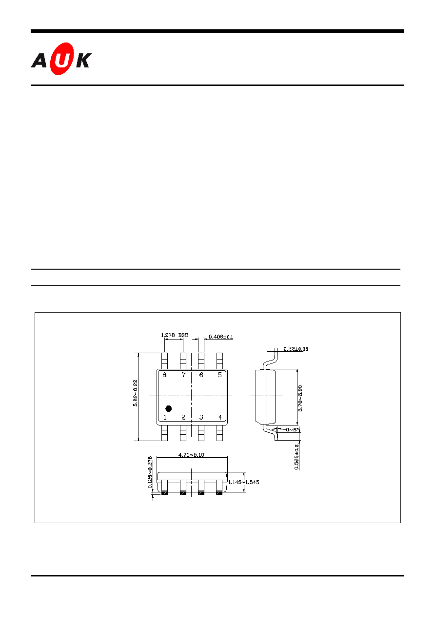
Outline Dimensions unit :
mm
S
S
e
e
m
m
i
i
c
c
o
o
n
n
d
d
u
u
c
c
t
t
o
o
r
r
KSI-W025-001
2
Maximum Ratings
(Ta = 25
°C)
Characteristics Symbol
Rating
Unit
Supply Voltage
Vcc
17
V
Input Voltage
V
IN
5 Vp-p
Operating Temperature
Tope
-20 ~ 75
°C
Storage Temperature
Tstg
-55 ~ 150
°C
Allowable Power Dissipation
Pd
270
mW
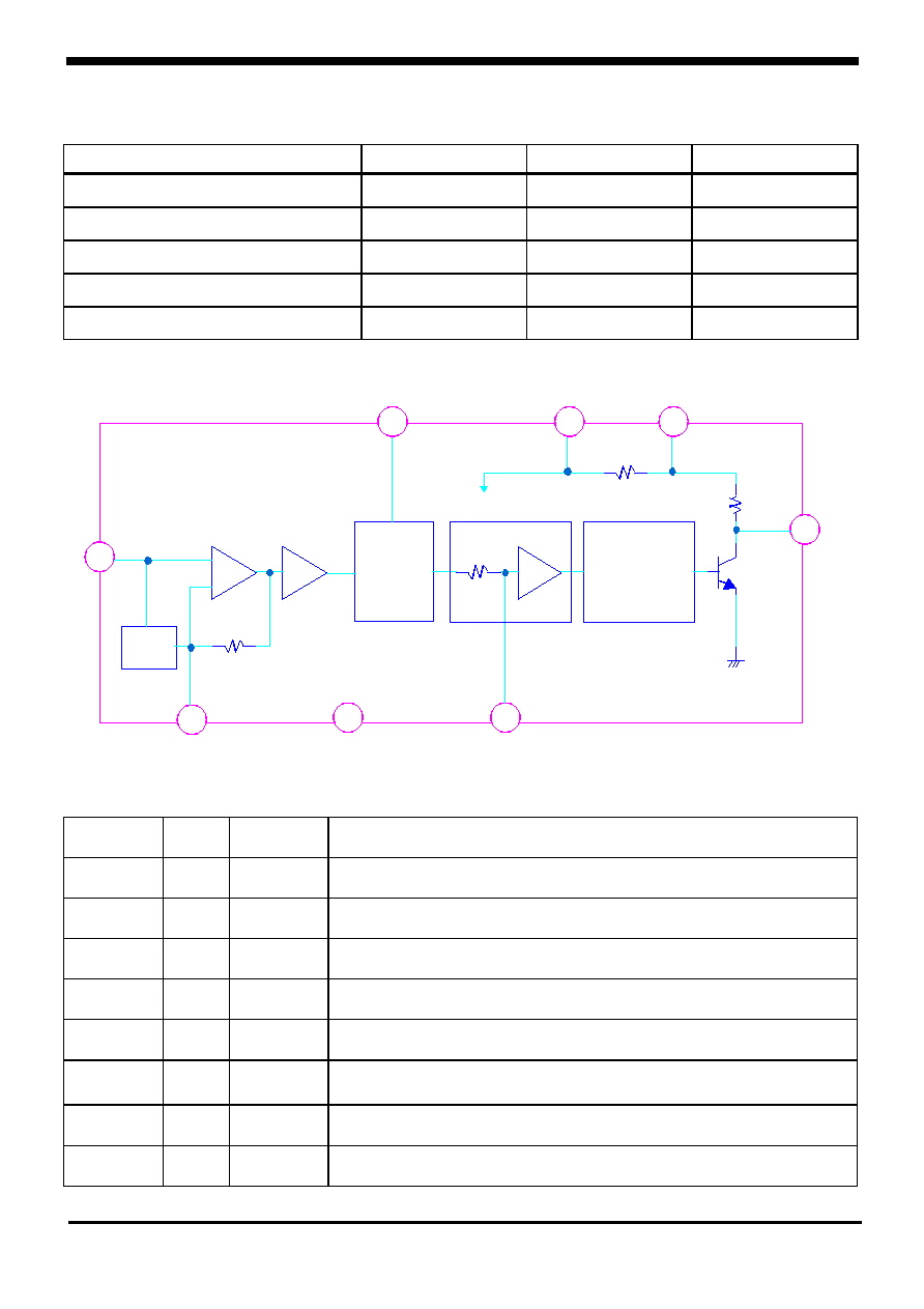
Block Diagram
PIN Description
Pin. No Symbol Pin Voltage
Description
1
Vcc1
5.0
The Power Supply Voltage
2
Out
5.0
Active Low Output Terminal and an Open Collector Output
3
Vcc2
The Power Output Voltage
4 fo 1.4
Setting
the
Center
Frequency of the Built-in BPF
5
GND
-
Ground
6 Cd 1.5
The Detection Capacitor for the most Output Pulse Width
Variation and Noise Reduction
7 IN- 2.5
Setting the Frequency Characteristics and Gain of the Head
Amplifier
8 IN+ 2.5
The
input
Signal Internal Impedance : 75K (typ.)
SL2055
1
2
3
4
5
7
8
IN+
W A V EF O R M
S HA P ER
A BLC
BP F
+
T R A P
V CC2
f o
6
R S
V CC1
R L
O UT
Cd
G ND
I N-
HEA D
A MP
LI MI T ER
DET ECT O R

KSI-W025-001
3
Electrical Characteristics(V
CC
=5V, Ta=25 °C)
Test Condition
Test
Rating
Item
Symbol
Input Signal
ON-SW
Pin
Min.
Typ. Max.
Unit Remark
Input Pin Vol1
Vin1
1
8
2.0
2.5
3.1
V
Input Pin Vol2
Vin2
Iin=300µA 1,4,6 8 0.6 0.9 1.7 V
Output Voltage
(Low Level)
VOL V
P6
=1V 3,5 2 -
0.2
0.4
V
Consumption
Current
I
CC
1,5
1
1.0
1.9
2.8
mA
Input Impedance
Zin
fin=38KHz,CW,
Vin=0.2V
PP
1,4,8 8 45 75 125
K Note1
Voltage Gain
Av
fin=38KHz
Vin=30µVpp
2,4,7,8 6 68 - 82 dB
BPF Bandwidth
f
BW
-3dB
Bandwidth
Vin=30µV
PP
2,4,7,8 6 1.0 - 2.0 KHz
Detecting Ability(1) T
PW1
fin=38KHz
Vin=60µV
PP
,
Burst Wave
1,4,7,8 2 440 540 770
µSec Note2
Detecting Ability(1) T
PW2
fin=38KHz
Vin=50mV
PP
,
Burst Wave
1,4,7,8 2 440 660 770
µSec Note2
Note)
1.Zin =75/[(Vi/Vx)-1] Vi : Input Level, Vx : Measured Value
2.Input a Burst Wave Signal of 1.2mSec Cycle, 38kHz
SL2055

KSI-W025-001
5
Terminal Functions
IN + (input pin)
Connect a photodiode with pin structure between the pin8 and GND.
An ABLC (Automatic Bias Level Control)circuit is built into the input section to prevent the
input level from being saturated by the external disturbing lights, such that this circuit is
actuated by a strong external disturbing light to fix the bias level of the input terminal.
IN (head amplifier gain setting pin)
Connect a resistor and a capacitor in series between the pin7 and GND for setting the
frequency characteristics and gain of the head amplifier.
Increasing the value of a resistor or decreasing the value of a capacitor, the gain becomes
small.
When the capacitance is large the sensitivity is lowered against the transient response.
Cd (detector capacitor connector pin)
Connect the capacitor to detect between the pin6 to GND.
When capacitance is large detected value is to the average, when it is small detected value
is closer to the peak and output pulse width became, so that the most proper output pulse
width variation and noise reduction characteristics can be obtained.
GND (ground pin)
Fo (BPF central or frequency setting pin)
Connect a resistor between the pin3 (V
CC
2) and the pin4
When the resistance is large, the central frequency of the built-in BPF is lowered.
V
CC
2 (power output pin)
As the power is output to pin3 through the internal power filter resistance, connect
An electrolytic capacitor to pin3
OUT (output pin)
Open collector output width pull-up resistance.
Its capability to drive a CMOS or TTL makes for easy connection with a receiving
microcomputer.
The SL2055 has an active low output
.
V
CC
1 (power supply pin)
Supply voltage of 5V±10% is applied to this terminal
SL2055