KSI-9020-001
1
S78DL33
Low Drop output Voltage Regulator
Descriptions
∑ Three Terminal Positive Low Dropout Voltage Regulator
Features
∑ Low Standby Current Consumption (500
Typ.)
∑ Maximum Output Current (180
Max.)
∑ Less I/O voltage Difference (250 Max.)
Ordering
Information
Type NO. Marking Package Code
S78DL33 S78DL33 TO-92
Outline Dimensions unit :
mm
4.5±0.1
4.
5
±
0.
1
0.4±0.02
1.27 Typ
.
2.54 Typ
.
1 2 3
3.45±0.1
2.25±0.1
2.06±0.1
1.
20
±
0.
1
0.
38
S
S
e
e
m
m
i
i
c
c
o
o
n
n
d
d
u
u
c
c
t
t
o
o
r
r
PIN Connections
1. Output
2. GND
3. Input
Functional Block Diagram

KSI-9020-001
2
S78DL33
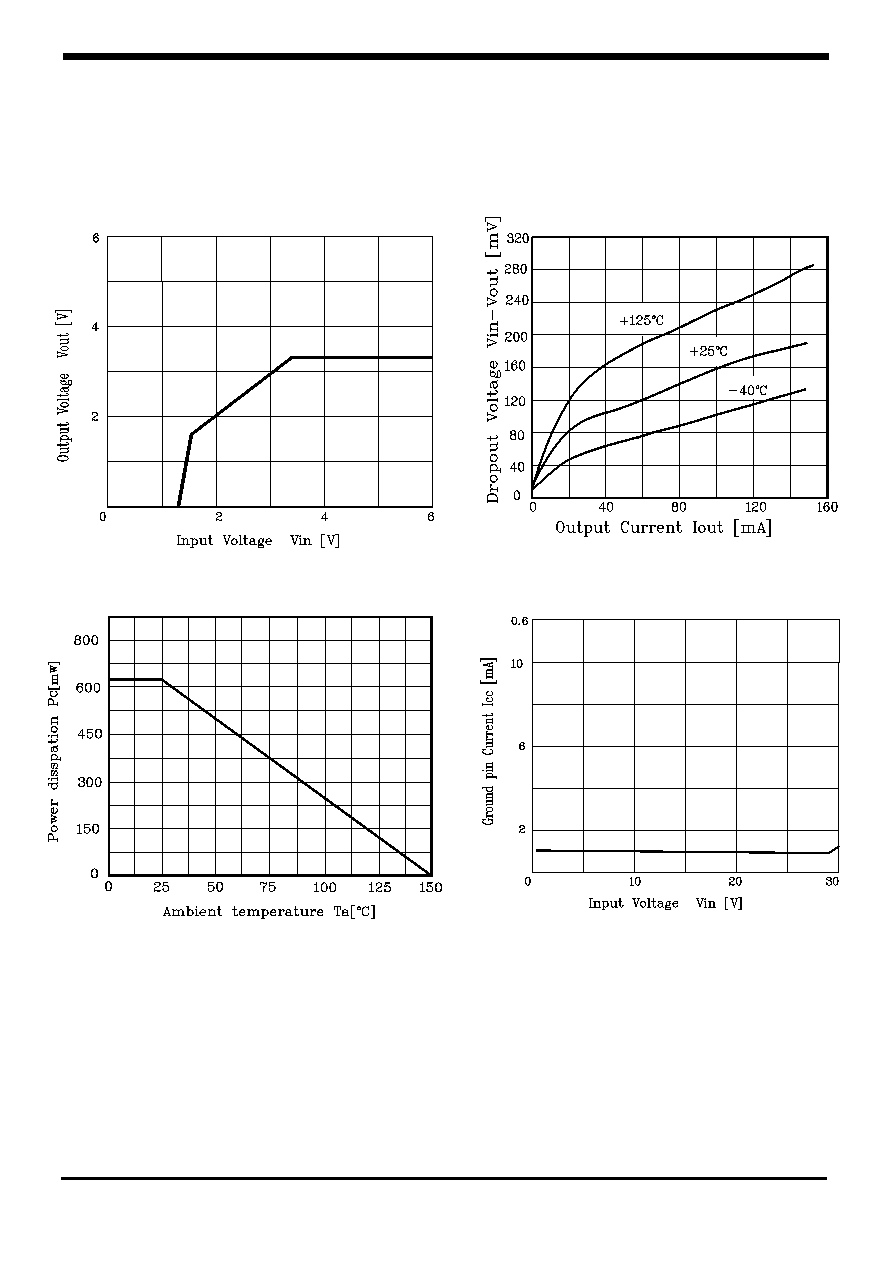
Maximum ratings
Ta=25
∞C
Characteristic Symbol
Ratings
Unit
Operating Input voltage
V
IN
16 V
Power Dissipation
P
D
625
mW
Operating Temperature Range
T
OPR
-40~+85 ∞C
Junction Temperature
T
j
150
∞C
Storage Temperature Range
T
stg
-55~150 ∞C
Lead Temperature Time
T
sol
260 (10 Sec)
∞C
Electrical Characteristics
( V
IN
=4.3V, I
OUT
=100uA, T
j
=25
∞C)
Characteristic Symbol Test
Condition Min.
Typ.
Max.
Unit
Output voltage
V
OUT
V
IN
=4.3V, I
OUT
=100uA
3.168
3.3
3.432
V
Voltage Regulation
V
OUT
(1) V
IN
=4.3V~10V, I
OUT
=100uA -
2
15
mV
Load Regulation
V
OUT
(2) V
IN
=4.3V , I
OUT
=1~100mA -
7
28
mV
I
OUT
=50mA -
110
230
Dropout Voltage
V
DROP
I
OUT
=100mA -
150
300
mV
Ripple Rejection Ratio
RR
f=100Hz, I
OUT
=100uA -
75
-
dB
V
IN
=4.3V , I
OUT
=100uA
200
400
uA
V
IN
=4.3V , I
OUT
=50mA
0.9
1.8
mA
Ground pin Current
I
GND
V
IN
=4.3V , I
OUT
=100mA
2.1
4
mA
Test circuit