KSI-K001-000
1
S324
Low Power Quad OP AMP
Description
The S324 consists of four independent high gain Internally frequency compensated
operational amplifiers designed to operate from a single power supply over a wide
range of voltage.
Features
∑ Input common mode voltage range includes ground
∑ Internally frequency compensated for unity gain
∑ Large DC voltage gain : 100dB
∑ Wide bandwidth for unity gain : 1 MHz
∑ Very low power consumption
∑ Wide supply voltage range : Single : 3V ~ 36V, Dual :
±
1.5 ~
±
18V
Applications
∑ Transducer amplifier
∑ DC gain blocks
∑ Conventional operational amplifiers
Ordering
Information
Type NO. Marking Package Code
S324 S324 SOP-14
Outline Dimensions unit :
mm
S
S
e
e
m
m
i
i
c
c
o
o
n
n
d
d
u
u
c
c
t
t
o
o
r
r
Block Diagram
KSI-K001-000
2
S324
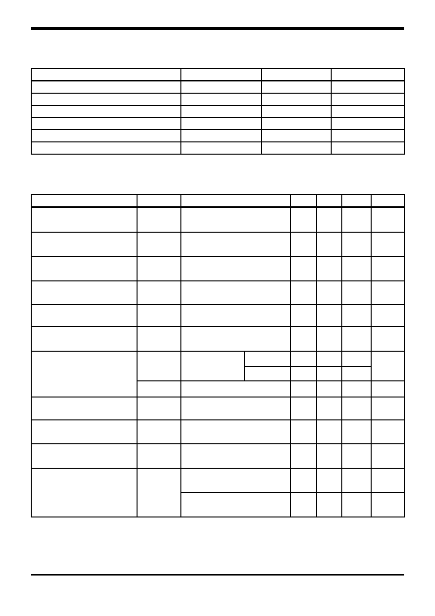
Absolute maximum ratings
Characteristic Symbol
Ratings
Unit
Supply voltage
V
CC
36
or
±
18 V
Differential input voltage
V
IND
36 V
Input voltage
V
IN
-0.3 ~ +36
V
Power Dissipation
P
D
300
mW
Operating temperature
T
opr
-40 ~ +85
∞C
Storage temperature
T
stg
-55 ~ 150
∞C
Electrical Characteristics
(Unless otherwise specified. V
CC
= 5V, V
EE
= GND and ≠40
∞C
Ta
+85
∞C
)
Characteristic Symbol Test
Condition Min.
Typ.
Max.
Unit
Input offset voltage
V
IOS
V
CC
= 5~30V
Rg = 0
- 2 7 mV
Input offset current
I
IOS
-
-
5
30
nA
Input bias current
I
IB
-
-
45
150
nA
Input common mode
voltage range
V
ICR
V
CC
= 30V
0
-
V
CC
≠1.5
V
Supply current
I
CC
R
L
= , All Channel
- 0.7 1.2 mA
Large signal voltage
gain
G
V
V
CC
= 15V
R
L
2 K
86 100 -
dB
V
CC
= 30V
R
L
=2 K
26 - -
V
OH
R
L
=10 K
27 28 -
V
Output voltage swing
V
OL
V
CC
=5V, R
L
10 K
- 5 20 mV
Common mode
rejection ratio
CMRR
(Ta=25 ∞C)
65 85 - dB
Power supply
rejection ratio
PSRR
(Ta=25 ∞C)
65 100 -
dB
Output source current
I
O+
V
CC
= 15V
V
IN+
= 1V, V
IN-
= 0V
20 40 - mA
V
CC
= 15V
V
IN+
= 0V, V
IN-
= 1V
10 20 - mA
Output sink current
I
O-
V
OUT
= 200mV,
V
IN+
= 0V, V
IN-
= 1V, V
CC
= 15V
12 45 -
µA