1
Features
∑
Ultra High Performance
≠ System Speeds to 100 MHz
≠ Array Multipliers > 50 MHz
≠ 10 ns Flexible SRAM
≠ Internal Tri-state Capability in Each Cell
∑
FreeRAM
TM
≠ Flexible, Single/Dual Port, Synchronous/Asynchronous 10 ns SRAM
≠ 2,048 - 18,432 Bits of Distributed SRAM Independent of Logic Cells
∑
128 - 384 PCI Compliant I/Os
≠ Programmable Output Drive
≠ Fast, Flexible Array Access Facilitates Pin Locking
≠ Pin-compatible with XC4000, XC5200 FPGAs
∑
8 Global Clocks
≠ Fast, Low Skew Clock Distribution
≠ Programmable Rising/Falling Edge Transitions
≠ Distributed Clock Shutdown Capability for Low Power Management
≠ Global Reset/Asynchronous Reset Options
≠ 4 Additional Dedicated PCI Clocks
∑
Cache Logic
Æ
Dynamic Full/Partial Re-configurability In-System
≠ Unlimited Re-programmability via Serial or Parallel Modes
≠ Enables Adaptive Designs
≠ Enables Fast Vector Multiplier Updates
≠ QuickChange
TM
Tools for Fast, Easy Design Changes
∑
Pin-compatible Package Options
≠ Plastic Leaded Chip Carriers (PLCC)
≠ Thin, Plastic Quad Flat Packs (LQFP, TQFP, PQFP)
≠ Ball Grid Arrays (SBGA)
∑
Industry-standard Design Tools
≠ Seamless Integration (Libraries, Interface, Full Back-annotation) with
Concept
Æ
, Everest, Exemplar
TM
, Mentor
Æ
, OrCAD
Æ
, Synario
TM
, Synopsys
Æ
,
Verilog
Æ
, Veribest
Æ
, Viewlogic
Æ
, Synplicity
Æ
≠ Timing Driven Placement & Routing
≠ Automatic/Interactive Multi-chip Partitioning
≠ Fast, Efficient Synthesis
≠ Over 75 Automatic Component Generators Create 1000s
of Reusable, Fully Deterministic Logic and RAM Functions
∑
Intellectual Property Cores
≠ Fir Filters, UARTs, PCI, FFT and Other System Level Functions
∑
Easy Migration to Atmel Gate Arrays for High Volume Production
∑
Supply Voltage 3.3V
∑
5V I/O Tolerant
5K - 50K Gates
Coprocessor
FPGA with
FreeRAM
TM
AT40K05AL
AT40K10AL
AT40K20AL
AT40K40AL
Rev. 2818D≠FPGA≠02/03
2
AT40KAL Series FPGA
2818D≠FPGA≠02/03
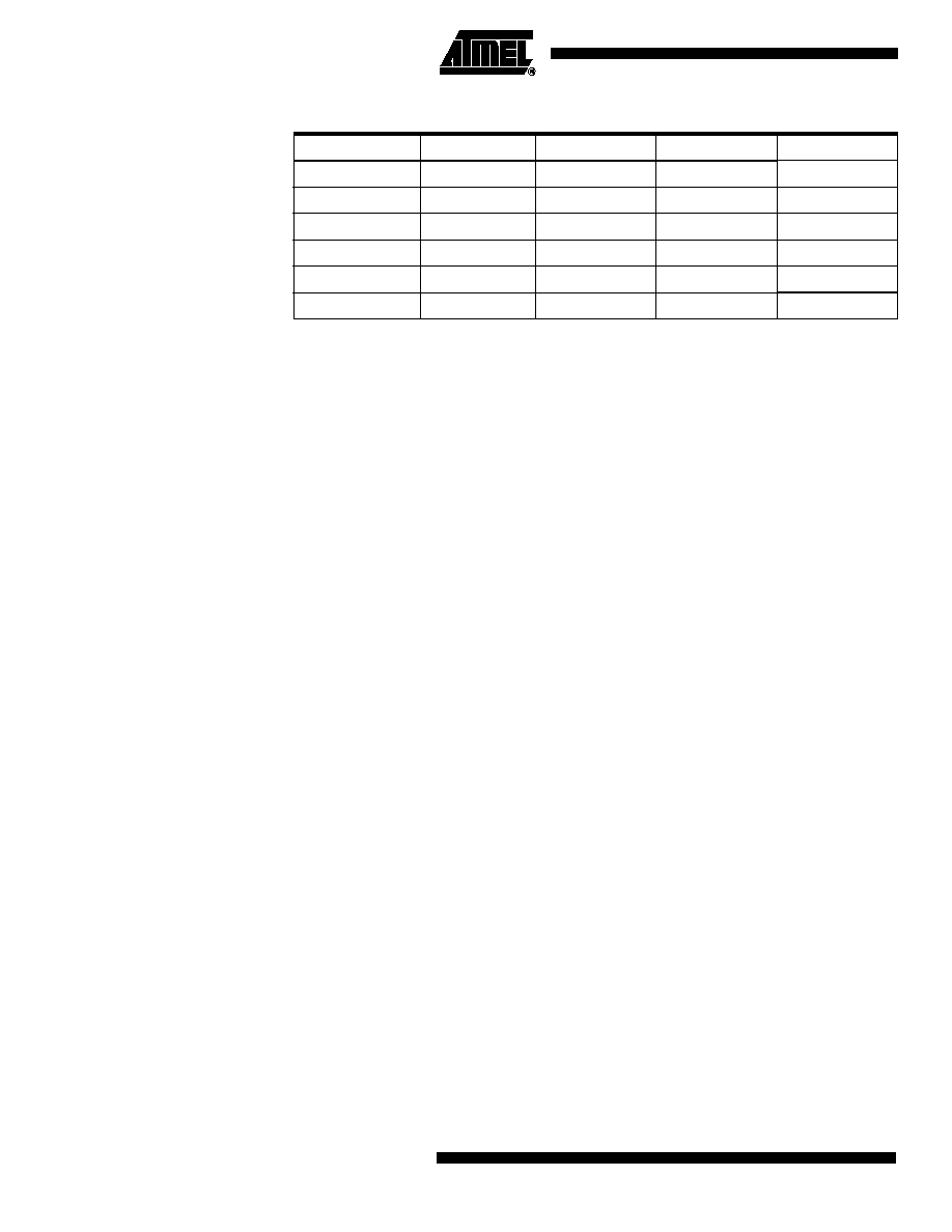
Note:
1. Packages with FCK will have 8 less registers.
Description
The AT40KAL is a family of fully PCI-compliant, SRAM-based FPGAs with distributed
10 ns programmable synchronous/asynchronous, dual-port/single-port SRAM, 8 global
clocks, Cache Logic ability (partially or fully reconfigurable without loss of data), auto-
matic component generators, and range in size from 5,000 to 50,000 usable gates. I/O
counts range from 128 to 384 in industry standard packages ranging from 84-pin PLCC
to 352-ball Square BGA, and support 3.3V designs.
The AT40KAL is designed to quickly implement high-performance, large gate count
designs through the use of synthesis and schematic-based tools used on a PC or Sun
platform. Atmel's design tools provide seamless integration with industry standard tools
such as Synplicity, ModelSim, Exemplar and Viewlogic. See the "IDS Datasheet" avail-
able on the Atmel web site (http://www.atmel.com/atmel/acrobat/doc1421.pdf) for a list
of other supported tools.
The AT40KAL can be used as a coprocessor for high-speed (DSP/processor-based)
designs by implementing a variety of computation intensive, arithmetic functions. These
include adaptive finite impulse response (FIR) filters, fast Fourier transforms (FFT), con-
volvers, interpolators and discrete-cosine transforms (DCT) that are required for video
compression and decompression, encryption, convolution and other multimedia
applications.
Fast, Flexible and
Efficient SRAM
The AT40KAL FPGA offers a patented distributed 10 ns SRAM capability where the
RAM can be used without losing logic resources. Multiple independent, synchronous or
asynchronous, dual-port or single-port RAM functions (FIFO, scratch pad, etc.) can be
created using Atmel's macro generator tool.
Fast, Efficient Array and
Vector Multipliers
The AT40KAL's patented 8-sided core cell with direct horizontal, vertical and diagonal
cell-to-cell connections implements ultra fast array multipliers without using any busing
resources. The AT40KAL's Cache Logic capability enables a large number of design
coefficients and variables to be implemented in a very small amount of silicon, enabling
vast improvement in system speed at much lower cost than conventional FPGAs.
Table 1. AT40KAL Family
(1)
Device
AT40K05AL
AT40K10AL
AT40K20AL
AT40K40AL
Usable Gates
5K - 10K
10K - 20K
20K - 30K
40K - 50K
Rows x Columns
16 x 16
24 x 24
32 x 32
48 x 48
Cells
256
576
1,024
2,304
Registers
496
(1)
954
(1)
1,520
(1)
3,048
(1)
RAM Bits
2,048
4,608
8,192
18,432
I/O (Maximum)
128
192
256
384
3
AT40KAL Series FPGA
2818D≠FPGA≠02/03
Cache Logic Design
The AT40KAL, AT6000 and FPSLIC families are capable of implementing Cache Logic
(dynamic full/partial logic reconfiguration, without loss of data, on-the-fly) for building
adaptive logic and systems. As new logic functions are required, they can be loaded into
the logic cache without losing the data already there or disrupting the operation of the
rest of the chip; replacing or complementing the active logic. The AT40KAL can act as a
reconfigurable coprocessor.
Automatic Component
Generators
The AT40KAL FPGA family is capable of implementing user-defined, automatically gen-
erated, macros in multiple designs; speed and functionality are unaffected by the macro
orientation or density of the target device. This enables the fastest, most predictable and
efficient FPGA design approach and minimizes design risk by reusing already proven
functions. The Automatic Component Generators work seamlessly with industry stan-
dard schematic and synthesis tools to create the fastest, most efficient designs
available.
The patented AT40KAL series architecture employs a symmetrical grid of small yet
powerful cells connected to a flexible busing network. Independently controlled clocks
and resets govern every column of cells. The array is surrounded by programmable I/O.
Devices range in size from 5,000 to 50,000 usable gates in the family, and have 256 to
3,048 registers. Pin locations are consistent throughout the AT40KAL series for easy
design migration in the same package footprint. The AT40KAL series FPGAs utilize a
reliable 0.35µ triple-metal, CMOS process and are 100% factory-tested. Atmel's PC-
and workstation-based integrated development system (IDS) is used to create
AT40KAL series designs. Multiple design entry methods are supported.
The Atmel architecture was developed to provide the highest levels of performance,
functional density and design flexibility in an FPGA. The cells in the Atmel array are
small, efficient and can implement any pair of Boolean functions of (the same) three
inputs or any single Boolean function of four inputs. The cell's small size leads to arrays
with large numbers of cells, greatly multiplying the functionality in each cell. A simple,
high-speed busing network provides fast, efficient communication over medium and
long distances.
4
AT40KAL Series FPGA
2818D≠FPGA≠02/03
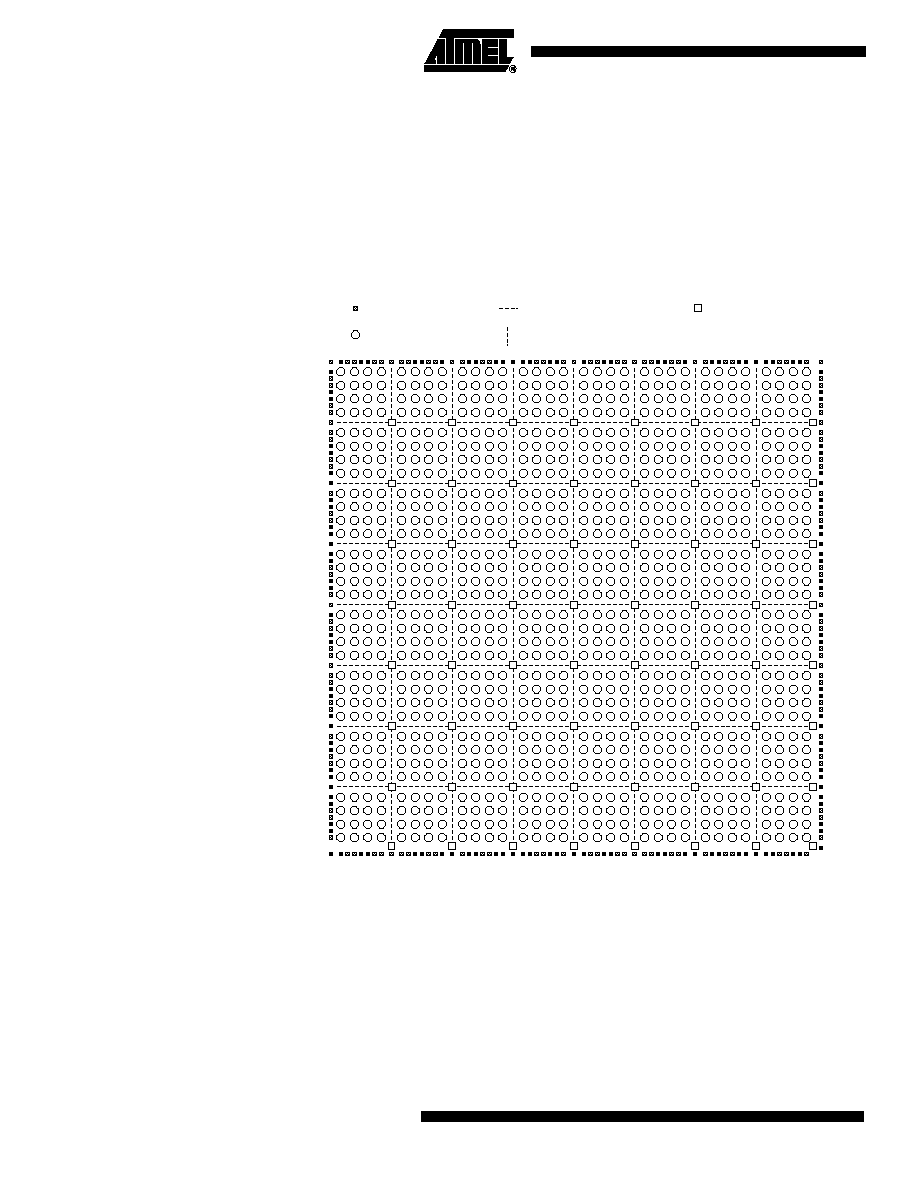
The Symmetrical
Array
At the heart of the Atmel architecture is a symmetrical array of identical cells,
see
Figure 1. The array is continuous from one edge to the other, except for bus
repeaters spaced every four cells, see Figure 2 on page 5. At the intersection of each
repeater row and column there is a 32 x 4 RAM block accessible by adjacent buses.
The RAM can be configured as either a single-ported or dual-ported RAM
(1)
, with either
synchronous or asynchronous operation.
Note:
1. The right-most column can only be used as single-port RAM.
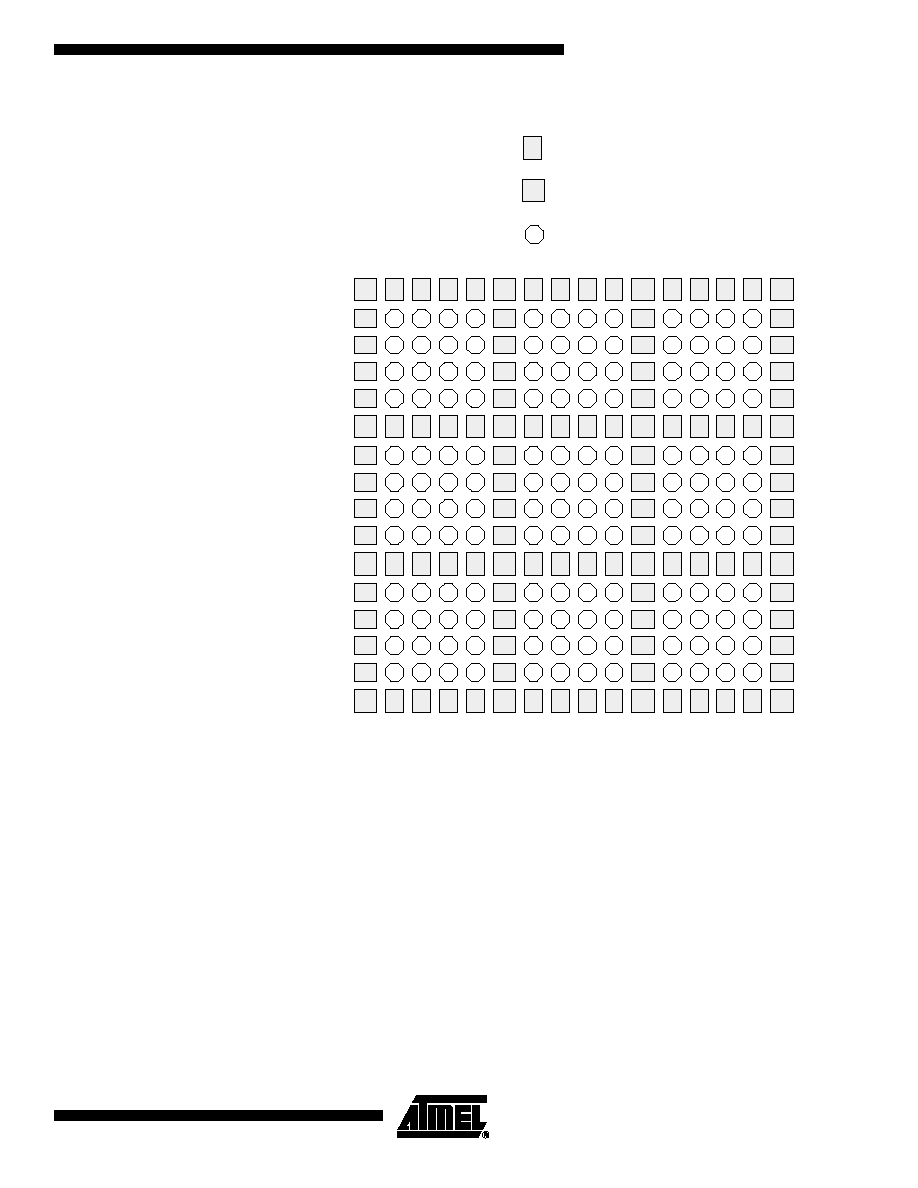
Figure 1. Symmetrical Array Surrounded by I/O (AT40K20AL)
(1)
Note:
1. AT40KAL has registered I/Os. Group enable on every sector for tri-states on obufe's.
= I/O Pad
= AT40K Cell
= Repeater Row
= Repeater Column
= FreeRAM
5
AT40KAL Series FPGA
2818D≠FPGA≠02/03
Figure 2. Floor Plan (Representative Portion)
(1)
Note:
1. Repeaters regenerate signals and can connect any bus to any other bus (all path-
ways are legal) on the same plane. Each repeater has connections to two adjacent
local-bus segments and two express-bus segments. This is done automatically using
the integrated development system (IDS) tool.
RH
RH
RH
RH
RH
RH
RH
RH
RH
RH
RH
RH
RH
RH
RH
RH
RH
RH
RH
RH
RH
RH
RH
RH
RH
RH
RH
RH
RH
RH
RH
RH
RH
RH
RH
RH
RH
RH
RH
RH
RH
RH
RH
RH
RH
RH
RH
RH
RV
RV
RV
RV
RV
RV
RV
RV
RV
RV
RV
RV
RV
RV
RV
RV
RV
RV
RV
RV
RV
RV
RV
RV
RV
RV
RV
RV
RV
RV
RV
RV
RV
RV
RV
RV
RV
RV
RV
RV
RV
RV
RV
RV
RV
RV
RV
RV
RV
RH
= Vertical Repeater
= Horizontal Repeater
= Core Cell
RAM
RAM
RAM
RAM
RAM
RAM
RAM
RAM
RAM
RAM
RAM
RAM
RAM
RAM
RAM
RAM