Äîêóìåíòàöèÿ è îïèñàíèÿ www.docs.chipfind.ru
Dual Enhancement Mode MOSFET (N-and P-Channel)
Copyright
ANPEC Electronics Corp.
Rev. B.1 - Mar., 2005
www.anpec.com.tw
1
ANPEC reserves the right to make changes to improve reliability or manufacturability without notice, and advise
customers to obtain the latest version of relevant information to verify before placing orders.
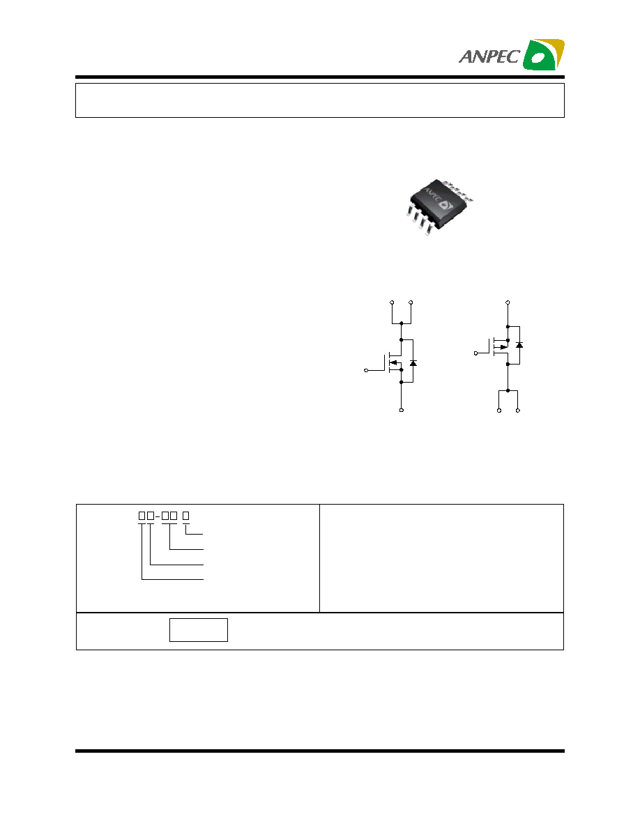
APM4532K
Features
Applications
·
Power Management in Notebook Computer,
Portable Equipment and Battery Powered
Systems
Pin Description
Ordering and Marking Information
N-Channel MOSFET
·
N-Channel
30V/5A,
R
DS(ON)
=35m
(typ.) @ V
GS
= 10V
R
DS(ON)
=60m
(typ.) @ V
GS
= 4.5V
··
··
·
P-Channel
-30V/-3.5A,
R
DS(ON)
=85m
(typ.) @ V
GS
=-10V
R
DS(ON)
=135m
(typ.) @ V
GS
=-4.5V
··
··
·
Super High Dense Cell Design
··
··
·
Reliable and Rugged
··
··
·
Lead Free Available (RoHS Compliant)
P-Channel MOSFET
G1
S1
S2
G2
D1
D1
D2
D2
APM4532
Handling Code
Tem p. Range
Package Code
Package Code
K : SOP-8
Operating Junction Tem p. Range
C : -55 to 150°C
Handling Code
TU : Tube TR : Tape & Reel
Lead Free Code
L : Lead Free Device Blank : Original Device
APM4532 K :
APM4532
XXXXX
XXXXX - Date Code
Lead Free Code
Top View of SOP
-
8
G 1
S 1
D 1
D 1
(8)
(7)
(2)
(1)
D 2
G 2
S 2
D 2
(4)
(3)
(5)
(6)
Note: ANPEC lead-free products contain molding compounds/die attach materials and 100% matte in plate termina-
tion finish; which are fully compliant with RoHS and compatible with both SnPb and lead-free soldiering operations.
ANPEC lead-free products meet or exceed the lead-free requirements of IPC/JEDEC J STD-020C for MSL classifica-
tion at lead-free peak reflow temperature.
Copyright
ANPEC Electronics Corp.
Rev. B.1 - Mar., 2005
www.anpec.com.tw
2
APM4532K
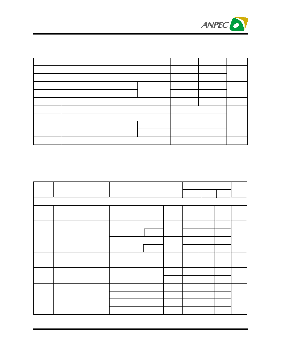
Absolute Maximum Ratings
(T
A
= 25
°
C unless otherwise noted)
Electrical Characteristics
(T
A
= 25
°
C unless otherwise noted)
Symbol
Parameter
N Channel
P Channel
Unit
V
DSS
Drain-Source Voltage
30 -30
V
GSS
Gate-Source Voltage
±20 ±20
V
I
D
*
Continuous Drain Current
5 -3.5
I
DM
*
Pulsed Drain Current
V
GS
=
±
10V
20 -14
A
I
S
*
Diode Continuous Forward Current
1.7 -1.7
A
T
J
Maximum Junction Temperature
150
T
STG
Storage Temperature Range
-55 to 150
°C
T
A
=25°C 2
P
D
*
Power Dissipation
T
A
=100°C
0.8
W
R
JA
*
Thermal Resistance-Junction to Ambient
62.5
°C/W
Note:
*Surface Mounted on 1in
2
pad area, t
10sec.
APM4532K
Symbol Parameter
Test
Condition
Min. Typ.
Max.
Unit
Static Characteristics
V
GS
=0V, I
DS
=250
µ
A
N-Ch 30
BV
DSS
Drain-Source Breakdown
Voltage
V
GS
=0V, I
DS
=-250
µ
A
P-Ch -30
V
V
DS
=24V, V
GS
=0V
1
T
J
=85°C
N-Ch
30
V
DS
=-24V, V
GS
=0V
-1
I
DSS
Zero Gate Voltage Drain
Current
T
J
=85°C
P-Ch
-30
µ
A
V
DS
=V
GS
, I
DS
=250
µ
A
N-Ch 1 1.5 2
V
GS(th)
Gate Threshold Voltage
V
DS
=V
GS
, I
DS
=-250
µ
A
P-Ch -1 -1.5 -2
V
N-Ch
±100
I
GSS
Gate Leakage Current
V
GS
=±20V, V
DS
=0V
P-Ch
±100
nA
V
GS
=10V, I
DS
=5A N-Ch
35
45
V
GS
=-10V, I
DS
=-3.5A P-Ch
85
95
V
GS
=4.5V, I
DS
=4A N-Ch
60
70
R
DS(ON)
a
Drain-Source On-State
Resistance
V
GS
=-4.5V, I
DS
=-2.5A P-Ch
135
150
m
Copyright
ANPEC Electronics Corp.
Rev. B.1 - Mar., 2005
www.anpec.com.tw
3
APM4532K
APM4532K
Symbol Parameter
Test
Condition
Min. Typ.
Max.
Unit
Diode Characteristics
I
SD
=1.7A, V
GS
=0V N-Ch
0.7
1.3
V
SD
a
Diode Forward Voltage
I
SD
=-1.7A, V
GS
=0V P-Ch
-0.7
-1.3
V
Dynamic Characteristics
b
N-Ch 3
R
G
Gate
Resistance
V
GS
=0V,V
DS
=0V,F=1MHz
P-Ch 13
N-Ch 440
C
iss
Input
Capacitance
P-Ch 530
N-Ch 90
C
oss
Output
Capacitance
P-Ch 90
N-Ch 40
C
rss
Reverse Transfer
Capacitance
N-Channel
V
GS
=0V,
V
DS
=25V,
Frequency=1.0MHz
P-Channel
V
GS
=0V,
V
DS
=-25V,
P-Ch 40
pF
N-Ch 10 15
t
d(ON)
Turn-on Delay Time
P-Ch 8 15
N-Ch 8 20
T
r
Turn-on Rise Time
P-Ch 7 20
N-Ch 20 28
t
d(OFF)
Turn-off Delay Time
P-Ch 15 28
N-Ch 5 15
T
f
Turn-off Fall Time
N-Channel
V
DD
=15V, R
L
=15
,
I
DS
=1A, V
GEN
=10V,
R
G
=6
P-Channel
V
DD
=-15V, R
L
=15
,
I
DS
=-1A, V
GEN
=-10V,
R
G
=6
P-Ch 7 18
ns
Gate Charge Characteristics
b
N-Ch 12.6
17
Q
g
Total Gate Charge
P-Ch 8 12
N-Ch 4.7
Q
gs
Gate-Source
Charge
P-Ch 2
N-Ch 1.1
Q
gd
Gate-Drain
Charge
N-Channel
V
DS
=15V, V
GS
=10V,
I
DS
=5A
P-Channel
V
DS
=-15V, V
GS
=-10V,
I
DS
=-3.5A
P-Ch 1
nC
Notes:
a : Pulse test ; pulse width
300
µ
s, duty cycle
2%.
b : Guaranteed by design, not subject to production testing.
Electrical Characteristics (Cont.)
(T
A
= 25
°
C unless otherwise noted)
Copyright
ANPEC Electronics Corp.
Rev. B.1 - Mar., 2005
www.anpec.com.tw
4
APM4532K
1E-4
1E-3
0.01
0.1
1
10 30
1E-3
0.01
0.1
1
2
Mounted on 1in
2
pad
R
JA
: 62.5
o
C/W
0.01
0.02
0.05
0.1
0.2
Single Pulse
Duty = 0.5
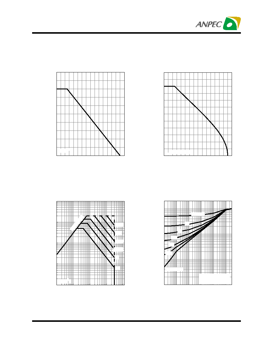
Typical Characteristics
I
D
- Drain Current (A)
Drain Current
T
j
- Junction Temperature (°C)
Safe Operation Area
V
DS
- Drain - Source Voltage (V)
Thermal Transient Impedance
Square Wave Pulse Duration (sec)
Power Dissipation
P
tot
- Power (W)
T
j
- Junction Temperature (°C)
I
D
- Drain Current (A)
N-Channel
0
20
40
60
80
100 120 140 160
0.0
0.5
1.0
1.5
2.0
2.5
T
A
=25
o
C
0
20
40
60
80
100 120 140 160
0
1
2
3
4
5
6
T
A
=25
o
C,V
G
=10V
0.01
0.1
1
10
100
0.01
0.1
1
10
100
R
ds(
on
) Li
mi
t
1s
T
A
=25
O
C
10ms
300
µ
s
1ms
100ms
DC
Normalized Transient Thermal Resistance
Copyright
ANPEC Electronics Corp.
Rev. B.1 - Mar., 2005
www.anpec.com.tw
5
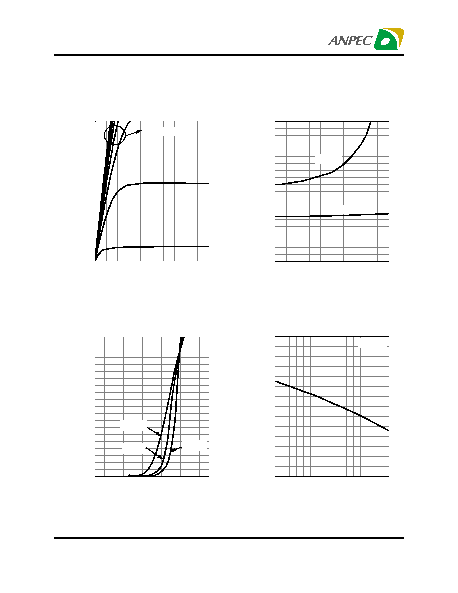
APM4532K
R
DS(ON)
- On - Resistance (m
)
Drain-Source On Resistance
I
D
- Drain Current (A)
T
j
- Junction Temperature (°C)
Gate Threshold Voltage
V
DS
- Drain-Source Voltage (V)
I
D
- Drain Current (A)
Output Characteristics
Transfer Characteristics
V
GS
- Gate - Source Voltage (V)
I
D
- Drain Current (A)
Normalized Threshold V
oltage
Typical Characteristics (Cont.)
N-Channel
0
1
2
3
4
5
0
2
4
6
8
10
12
14
16
18
20
3V
4V
V
GS
=5,6,7,8,9,10V
0
4
8
12
16
20
0
10
20
30
40
50
60
70
80
90
100
V
GS
=10V
V
GS
=4.5V
0
1
2
3
4
5
6
0
2
4
6
8
10
12
14
16
18
20
T
j
=125
o
C
T
j
=25
o
C
T
j
=-55
o
C
-50
-25
0
25
50
75
100 125 150
0.2
0.4
0.6
0.8
1.0
1.2
1.4
1.6
I
DS
=250
µ