Äîêóìåíòàöèÿ è îïèñàíèÿ www.docs.chipfind.ru
N-Channel Enhancement Mode MOSFET
Copyright
ANPEC Electronics Corp.
Rev. B.1 - Mar., 2005
www.anpec.com.tw
1
ANPEC reserves the right to make changes to improve reliability or manufacturability without notice, and advise
customers to obtain the latest version of relevant information to verify before placing orders.
APM2030NV
A P M 2 0 3 0 N
H a n d lin g C o d e
T e m p . R a n g e
P a c k a g e C o d e
P a c k a g e C o d e
V : S O T -2 2 3
O p e ra tin g J u n c tio n T e m p . R a n g e
C : -5 5 to 1 5 0 °C
H a n d lin g C o d e
T U : T u b e T R : T a p e & R e e l
L e a d F re e C o d e
L : L e a d F re e D e v ic e B la n k : O rig in a l D e v ic e
A P M 2 0 3 0 N V :
A P M 2 0 3 0 N
X X X X X
X X X X X - D a te C o d e
L e a d F re e C o d e
Pin Description
Ordering and Marking Information
Features
Applications
·
20V/6A ,
R
DS(ON)
=28m
(typ.) @ V
GS
=4.5V
R
DS(ON)
=38m
(typ.) @ V
GS
=2.5V
··
··
·
Super High Dense Cell Design
··
··
·
Reliable and Rugged
··
··
·
Lead Free Available (RoHS Compliant)
·
Switching Regulators
··
··
·
Switching Converters
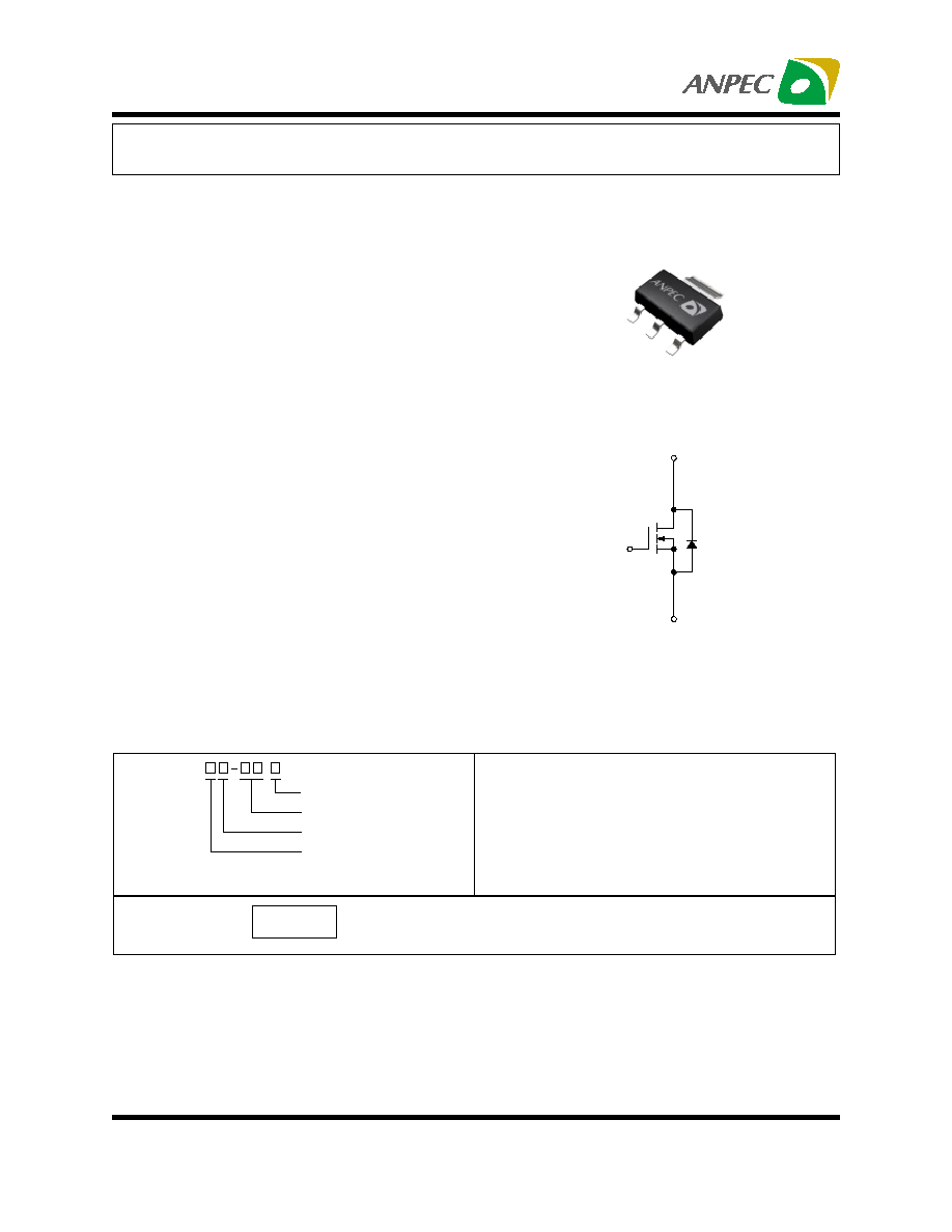
Top View of SOT-223
N-Channel MOSFET
G
D
S
G
S
D
(3)
(2)
(1)
Note: ANPEC lead-free products contain molding compounds/die attach materials and 100% matte in plate termina-
tion finish; which are fully compliant with RoHS and compatible with both SnPb and lead-free soldiering operations.
ANPEC lead-free products meet or exceed the lead-free requirements of IPC/JEDEC J STD-020C for MSL classifica-
tion at lead-free peak reflow temperature.
Copyright
ANPEC Electronics Corp.
Rev. B.1 - Mar., 2005
www.anpec.com.tw
2
APM2030NV
Symbol Parameter Rating
Unit
V
DSS
Drain-Source Voltage
20
V
GSS
Gate-Source Voltage
±12
V
I
D
*
Continuous Drain Current
6
I
DM
*
Pulsed Drain Current
V
GS
=4.5V
24
A
I
S
*
Diode Continuous Forward Current
2.3
A
T
J
Maximum Junction Temperature
150
T
STG
Storage Temperature Range
-55 to 150
°C
T
A
=25°C
1.47
P
D
*
Power Dissipation for Single Operation
T
A
=100°C
0.58
W
R
JA
*
Thermal Resistance-Junction to Ambient
85
°C/W
Note:
*Surface Mounted on 1in
2
pad area, t
10sec.
APM2030NV
Symbol Parameter
Test
Condition
Min. Typ. Max.
Unit
Static Characteristics
BV
DSS
Drain-Source Breakdown Voltage
V
GS
=0V, I
DS
=250
µ
A
20 V
V
DS
=16V, V
GS
=0V
1
I
DSS
Zero Gate Voltage Drain Current
T
J
=85°C
30
µ
A
V
GS(th)
Gate Threshold Voltage
V
DS
=V
GS
, I
DS
=250
µ
A
0.5 0.7 1 V
I
GSS
Gate Leakage Current
V
GS
=±12V, V
DS
=0V
±100
nA
V
GS
=4.5V, I
DS
=6A
28
32
R
DS(ON)
a
Drain-Source On-state Resistance
V
GS
=2.5V, I
DS
=2A
38
45
m
V
SD
a
Diode Forward Voltage
I
SD
=1.5A, V
GS
=0V
0.7
1.3
V
Gate Charge Characteristics
b
Q
g
Total Gate Charge
9
11
Q
gs
Gate-Source
Charge
3.6
Q
gd
Gate-Drain
Charge
V
DS
=10V, V
GS
=4.5V,
I
DS
=6A
1
nC
Electrical Characteristics
(T
A
= 25
°
C unless otherwise noted)
Absolute Maximum Ratings
(T
A
= 25
°
C unless otherwise noted)
Copyright
ANPEC Electronics Corp.
Rev. B.1 - Mar., 2005
www.anpec.com.tw
3
APM2030NV
APM2030NV
Symbol Parameter
Test
Condition
Min. Typ. Max.
Unit
Dynamic Characteristics
b
R
G
Gate
Resistance
V
GS
=0V,V
DS
=0V,F=1MHz 2
C
iss
Input
Capacitance
520
C
oss
Output
Capacitance
110
C
rss
Reverse Transfer Capacitance
V
GS
=0V,
V
DS
=15V,
Frequency=1.0MHz
70
pF
t
d(ON)
Turn-on Delay Time
17
32
T
r
Turn-on Rise Time
15
29
t
d(OFF)
Turn-off Delay Time
45
56
T
f
Turn-off Fall Time
V
DD
=10V, R
L
=10
,
I
DS
=1A, V
GEN
=4.5V,
R
G
=6
25
32
ns
Notes:
a : Pulse test ; pulse width
300
µ
s, duty cycle
2%.
b : Guaranteed by design, not subject to production testing.
Electrical Characteristics (Cont.)
(T
A
= 25
°
C unless otherwise noted)
Copyright
ANPEC Electronics Corp.
Rev. B.1 - Mar., 2005
www.anpec.com.tw
4
APM2030NV
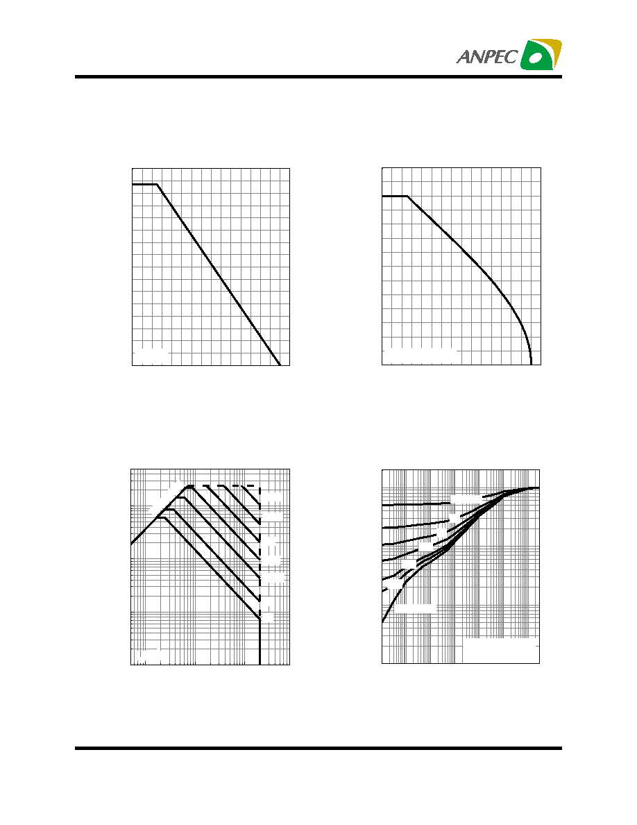
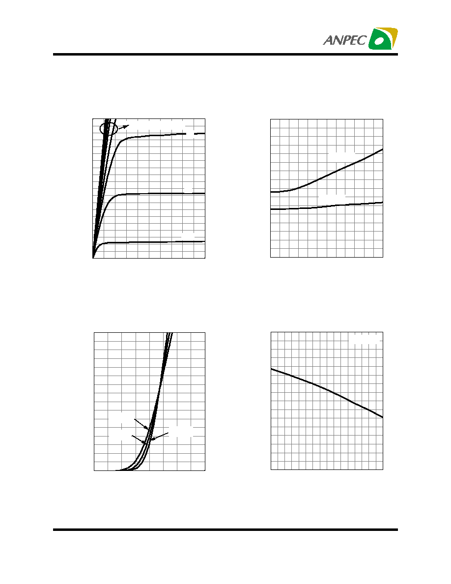
Typical Characteristics
Power Dissipation
P
tot
- Power (W)
T
j
- Junction Temperature (°C)
I
D
- Drain Current (A)
Drain Current
T
j
- Junction Temperature (°C)
Safe Operation Area
V
DS
- Drain - Source Voltage (V)
I
D
- Drain Current (A)
Normalized Transient Thermal Resistance
Thermal Transient Impedance
Square Wave Pulse Duration (sec)
0
20
40
60
80
100 120 140 160
0.0
0.2
0.4
0.6
0.8
1.0
1.2
1.4
1.6
T
A
=25
o
C
0
20
40
60
80
100 120 140 160
0
1
2
3
4
5
6
7
T
A
=25
o
C,V
G
=4.5V
1E-4 1E-3
0.01
0.1
1
10
100
1E-3
0.01
0.1
1
2
Mounted on 1in
2
pad
R
JA
: 85
o
C/W
0.01
0.02
0.05
0.1
0.2
Single Pulse
Duty = 0.5
0.1
1
10
80
0.01
0.1
1
10
50
R
ds(
on
) Li
m
it
100ms
300
µ
s
T
C
=25
o
C
1s
100
µ
s
1ms
10ms
DC
Copyright
ANPEC Electronics Corp.
Rev. B.1 - Mar., 2005
www.anpec.com.tw
5
APM2030NV
V
DS
- Drain - Source Voltage (V)
I
D
- Drain Current (A)
Output Characteristics
R
DS(ON)
- On - Resistance (m
)
Drain-Source On Resistance
I
D
- Drain Current (A)
Transfer Characteristics
V
GS
- Gate - Source Voltage (V)
I
D
- Drain Current (A)
T
j
- Junction Temperature (°C)
Gate Threshold Voltage
Normalized Threshold Vlotage
Typical Characteristics (Cont.)
0
1
2
3
4
5
0
2
4
6
8
10
12
14
16
18
20
3V
1.5V
2V
V
GS
=4,5,6,7,8,9,10V
0
4
8
12
16
20
24
0
10
20
30
40
50
60
70
80
V
GS
=4.5V
V
GS
=2.5V
0
1
2
3
4
0
3
6
9
12
15
18
21
24
T
j
=125
o
C
T
j
=25
o
C
T
j
=-55
o
C
-50
-25
0
25
50
75
100 125 150
0.0
0.2
0.4
0.6
0.8
1.0
1.2
1.4
1.6
I
DS
=250
µ
A
Copyright
ANPEC Electronics Corp.
Rev. B.1 - Mar., 2005
www.anpec.com.tw
6
APM2030NV
Drain-Source On Resistance
Normalized On Resistance
T
j
- Junction Temperature (°C)
V
SD
- Source - Drain Voltage (V)
Source-Drain Diode Forward
I
S
- Source Current (A)
V
DS
- Drain - Source Voltage (V)
C - Capacitance (pF)
Capacitance
Gate Charge
Q
G
- Gate Charge (nC)
V
GS
- Gate-source V
oltage (V)
Typical Characteristics (Cont.)
-50
-25
0
25
50
75
100 125 150
0.2
0.4
0.6
0.8
1.0
1.2
1.4
1.6
1.8
2.0
R
ON
@T
j
=25
o
C: 28m
V
GS
= 4.5V
I
DS
= 6A
0.0
0.2
0.4
0.6
0.8
1.0
1.2
1.4
1.6
0.1
1
10
20
T
j
=150
o
C
T
j
=25
o
C
0
4
8
12
16
20
0
100
200
300
400
500
600
700
800
Frequency=1MHz
Crss
Coss
Ciss
0
4
8
12
16
20
24
0
2
4
6
8
10
V
DS
=10V
I
D
= 6A
Copyright
ANPEC Electronics Corp.
Rev. B.1 - Mar., 2005
www.anpec.com.tw
7
APM2030NV
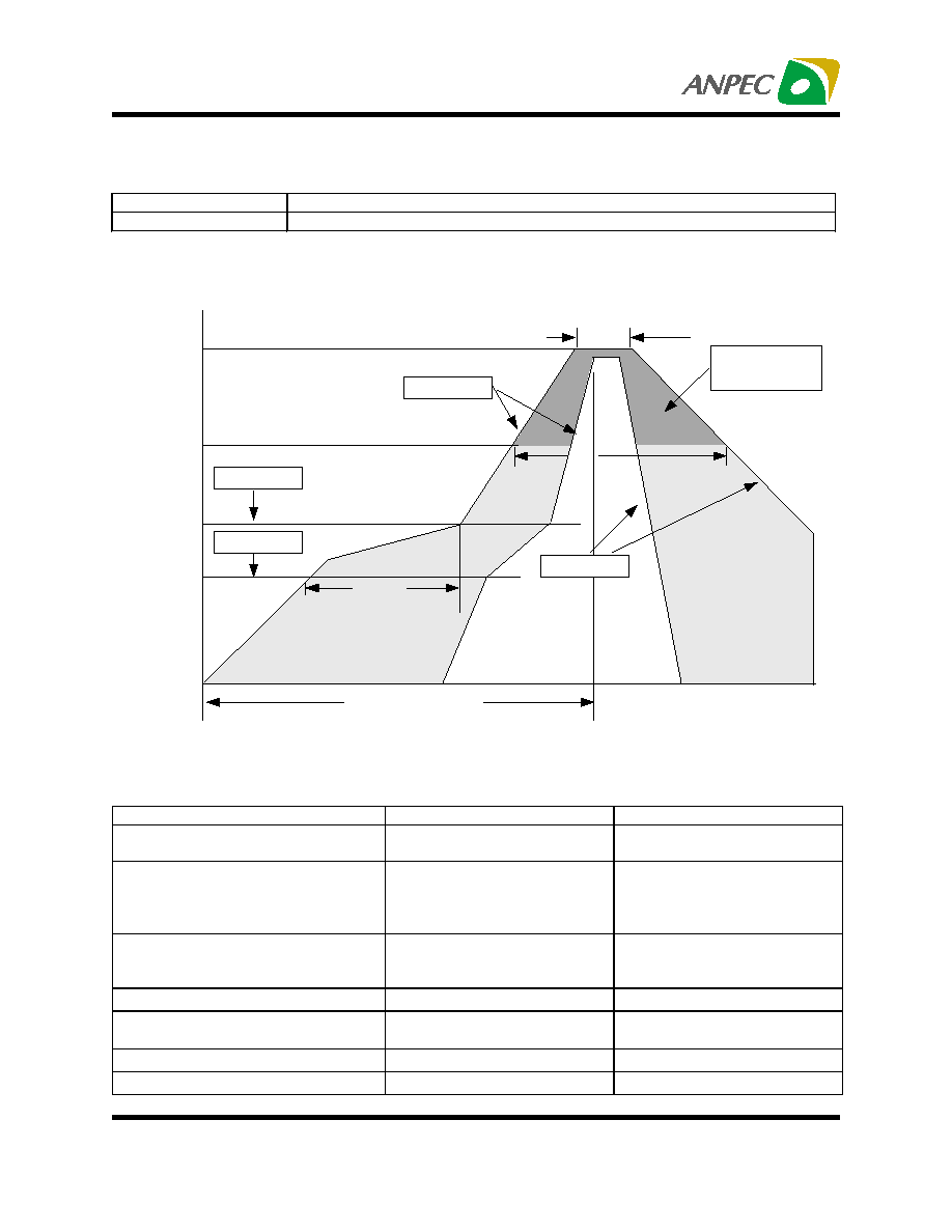
Millimeters Inches
Dim
Min. Max. Min. Max.
A 1.40
1.60
0.055
0.063
B 0.40
0.56
0.016
0.022
B1 0.35 0.48
0.014
0.019
C 0.35
0.44
0.014
0.017
D 4.40
4.60
0.173
0.181
D1 1.35 1.83
0.053
0.072
e
1.50 BSC
0.059 BSC
e1
3.00 BSC
0.118 BSC
E 2.29
2.60
0.090
0.102
H 3.75
4.25
0.148
0.167
L 0.80
1.20
0.031
0.047
10
°
10
°
Packaging Information
SOT-89 (Reference EIAJ ED-7500A Registration SC-62)
D
D 1
e
B 1
e 1
B
1
2
3
L
H
E
A
C
Copyright
ANPEC Electronics Corp.
Rev. B.1 - Mar., 2005
www.anpec.com.tw
8
APM2030NV
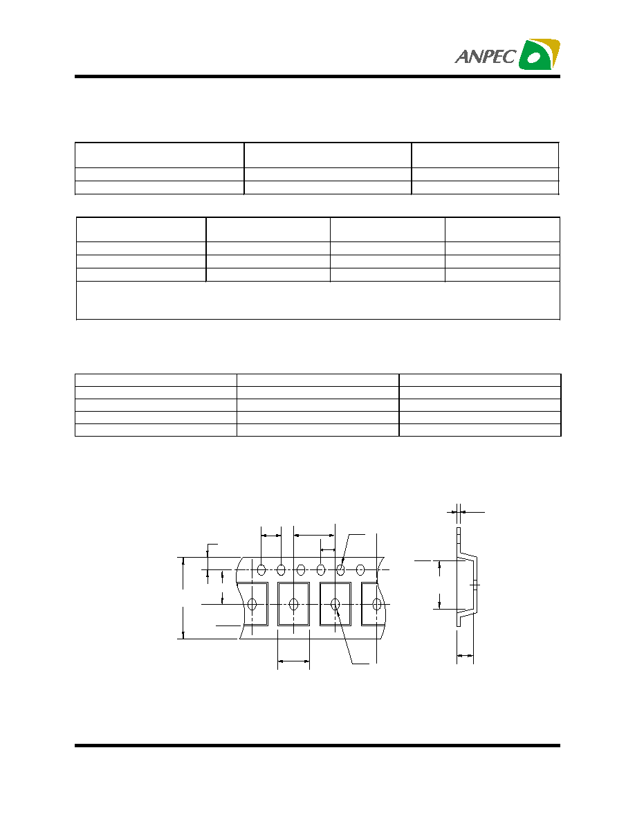
M i l l im e t e r s I n c he s
D i m
M i n . M a x .
M i n .
A 1 . 5 0
1 . 8 0 A 1 . 5 0
A 1 0 . 0 2 0 . 0 8 A 1 0 . 0 2
B 0 . 6 0
0 . 8 0 B 0 . 6 0
B 1 2 . 9 0 3 . 1 0 B 1 2 . 9 0
c 0 . 2 8
0 . 3 2 c 0 . 2 8
D 6 . 3 0
6 . 7 0 D 6 . 3 0
e 2 . 3
B S C
0 . 0 9
B S C
e 1 4 . 6
BSC
0 . 1 8
B S C
H 6 . 7 0
7 . 3 0 H 6 . 7 0
L 0 . 9 1
1 . 1 0 L 0 . 9 1
K 1 . 5 0
2 . 0 0 K 1 . 5 0
0
°
1 0
°
0
°
1 3
°
1 3
°
Packaging Information
SOT-223 (Reference JEDEC Registration SOT-223)
1.5
T YP
[0.06]
1 T YP
[0.04]
2.3
[0.092]
3.3
[0.132]
1.5
[0.06]
6.3
[0.252]
A
c
L
A
1
B
B
1
D
H
E
K
e
e
1
LA N D PA T T E R N
R E C O M M E N D A T IO N
C O N T R O LLIN G D IM E N S IO N
IS M ILLIM E T E R S V ALU E S IN
[ ] A R E IN C H
Copyright
ANPEC Electronics Corp.
Rev. B.1 - Mar., 2005
www.anpec.com.tw
9
APM2030NV
Physical Specifications
t 25 C to P e ak
tp
R am p-u p
t
L
R am p-d ow n
ts
P rehea t
T sm ax
T sm in
T
L
T
P
25
Tem
p
er
at
ur
e
T im e
C ritical Z one
T
L
to T
P
°
Terminal Material
Solder-Plated Copper (Solder Material : 90/10 or 63/37 SnPb), 100%Sn
Lead Solderability
Meets EIA Specification RSI86-91, ANSI/J-STD-002 Category 3.
Reflow Condition
(IR/Convection or VPR Reflow)
Classification Reflow Profiles
Profile Feature
Sn-Pb Eutectic Assembly
Pb-Free Assembly
Average ramp-up rate
(T
L
to T
P
)
3
°
C/second max.
3
°
C/second max.
Preheat
-
Temperature Min (Tsmin)
-
Temperature Max (Tsmax)
-
Time (min to max) (ts)
100
°
C
150
°
C
60-120 seconds
150
°
C
200
°
C
60-180 seconds
Time maintained above:
-
Temperature (T
L
)
-
Time (t
L
)
183
°
C
60-150 seconds
217
°
C
60-150 seconds
Peak/Classificatioon Temperature (Tp)
See table 1
See table 2
Time within 5
°
C of actual
Peak Temperature (tp)
10-30 seconds
20-40 seconds
Ramp-down Rate
6
°
C/second max.
6
°
C/second max.
Time 25
°
C to Peak Temperature
6 minutes max.
8 minutes max.
Notes: All temperatures refer to topside of the package .Measured on the body surface.
Copyright
ANPEC Electronics Corp.
Rev. B.1 - Mar., 2005
www.anpec.com.tw
10
APM2030NV
Test item
Method
Description
SOLDERABILITY
MIL-STD-883D-2003
245°C,5 SEC
HOLT
MIL-STD 883D-1005.7
1000 Hrs Bias @ 125°C
PCT
JESD-22-B, A102
168 Hrs, 100% RH, 121°C
TST
MIL-STD 883D-1011.9
-65°C ~ 150°C, 200 Cycles
Carrier Tape & Reel Dimensions
t
A o
E
W
P o
P
K o
B o
D 1
D
F
P 1
Reliability Test Program
Table 2. Pb-free Process Package Classification Reflow Tem peratures
Package Thickness
Volum e m m
3
<350
Volum e m m
3
350-2000
Volum e m m
3
>2000
<1.6 m m
260 +0
°
C* 260
+0
°
C* 260
+0
°
C*
1.6 m m 2.5 m m
260 +0
°
C* 250
+0
°
C* 245
+0
°
C*
2.5 m m
250 +0
°
C* 245
+0
°
C* 245
+0
°
C*
*Tolerance: The device m anufacturer/supplier shall assure process com patibility up to and
including the stated classification tem perature (this m eans Peak reflow tem perature +0
°
C.
For exam ple 260
°
C+0
°
C) at the rated M SL level.
Table 1. SnPb Entectic Process Package Peak R eflow Tem peratures
Package Thickness
Volum e m m
3
<350
Volum e m m
3
350
<2.5 m m
240 +0/-5
°
C 225
+0/-5
°
C
2.5 m m
225 +0/-5
°
C 225
+0/-5
°
C
Classification Reflow Profiles(Cont.)
Copyright
ANPEC Electronics Corp.
Rev. B.1 - Mar., 2005
www.anpec.com.tw
11
APM2030NV
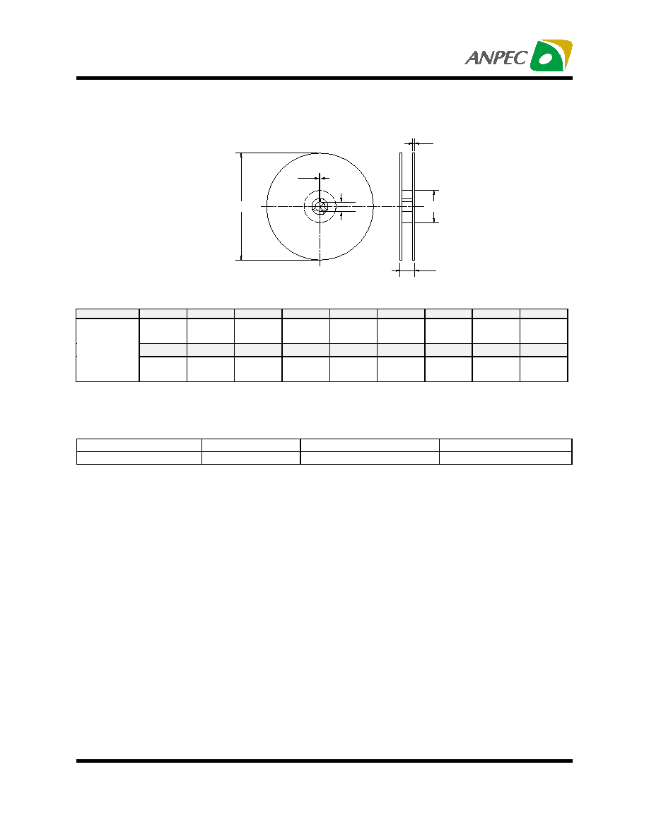
Application
A
B
C
J
T1
T2
W
P
E
330
±
3
100
±
2
13
±
0. 5
2
±
0.5
16.4 + 0.3
-0.2
2.5
±
0.5
16+ 0.3
- 0.1
8
±
0.1
1.75
±
0.1
F
D
D1
Po
P1
Ao
Bo
Ko
t
TO-252
7.5
±
0.1
1.5 +0.1
1.5
±
0.25
4.0
±
0.1
2.0
±
0.1
6.8
±
0.1
10.4
±
0.1
2.5
±
0.1
0.3
±
0.05
Application
Carrier Width
Cover Tape Width
Devices Per Reel
TO- 252
16
13.3
2500
Customer Service
Anpec Electronics Corp.
Head Office :
5F, No. 2 Li-Hsin Road, SBIP,
Hsin-Chu, Taiwan, R.O.C.
Tel : 886-3-5642000
Fax : 886-3-5642050
Taipei Branch :
7F, No. 137, Lane 235, Pac Chiao Rd.,
Hsin Tien City, Taipei Hsien, Taiwan, R. O. C.
Tel : 886-2-89191368
Fax : 886-2-89191369
Cover Tape Dimensions
Carrier Tape & Reel Dimensions (Cont.)
A
J
B
T 2
T 1
C
(mm)